
Microwave-annealing-induced nanowetting of block copolymers in cylindrical nanopores†
Chun-Wei
Chang
,
Ming-Hsiang
Cheng
,
Hao-Wen
Ko
,
Chien-Wei
Chu
,
Yi-Hsuan
Tu
and
Jiun-Tai
Chen
 *
*
Department of Applied Chemistry, National Chiao Tung University, Hsinchu 30010, Taiwan. E-mail: jtchen@mail.nctu.edu.tw
First published on 27th November 2017
Abstract
Block copolymers have attracted great attention because of their abilities to self-assemble into well-ordered microphase-separated structures. To generate nanopatterns of block copolymers with long-range ordering and low-defect densities in shorter time scales, microwave annealing has recently been applied. Microwave annealing, however, has so far only been used for block copolymer bulks and thin films. In this work, we discover that microwave annealing can be successfully applied to three-dimensional block copolymer nanostructures by studying the infiltration and microphase separation of block copolymers in cylindrical nanopores upon microwave irradiation. Cylinder-forming and lamella-forming poly(styrene-block-dimethylsiloxane) (PS-b-PDMS) are introduced into the nanopores of anodic aluminum oxide (AAO) templates. In addition, AAO templates with different pore sizes are used to study the effect of the commensurabilities between the pore diameters and the repeating periods of the block copolymers on the morphologies of the block copolymer nanostructures.
Introduction
Block copolymers have attracted considerable attention for decades because they can self-assemble into well-ordered nanostructures. The self-assembled morphologies of block copolymers including spheres, cylinders, gyroids, and lamellae can be controlled by different factors such as the molecular weight, the volume fraction, and the Flory–Huggins parameter (χ).1–3 The self-assembled nanostructures of block copolymers have been applied in different areas such as photovoltaics, sensors, drug delivery, and semiconductor manufacturing.4–9 To generate well-ordered self-assembled nanostructures of block copolymers for practical uses, annealing techniques such as thermal annealing and solvent vapor annealing have been frequently applied.10–13Recently, microwave annealing techniques have been used to control the morphologies of block copolymer bulks and thin films, inducing microphase separation in shorter processing times than those using the traditional thermal and solvent annealing techniques. For example, Zhang et al. annealed poly(styrene-block-methyl methacrylate) (PS-b-PMMA) and poly(styrene-block-2-vinylpyridine) (PS-b-P2VP) thin films cast on silicon wafers by microwave irradiation with the help of solvent vapor.14 The self-assembly behaviors of block copolymers were found to be significantly affected by the annealing conditions such as the annealing temperature, the type of solvent, and the resistivity of the substrate.14 One of the most important features is the selective heating mechanism; localized heating of materials is able to be achieved using microwave absorbers. For example, Jin et al. reported the heating mechanism of the microwave annealing processes on block copolymer thin films.15 A fiber optic temperature probe was used to monitor the in situ annealing temperature during the microwave annealing process. Their results reveal that the substrate underlying the polymer film is a key factor to determine the heating rate. When microwave-responsive materials such as lightly doped silicon are used, the substrate provides facile processing ability; when non-microwave-responsive materials such as Kapton plastic and glass are used, the heating rate is much slower. With further investigations on studying binary polymer blends, polymer brushes, and the type of heating elements, microwave annealing has been proven as a promising technique for block copolymer post-treatments to achieve nanopatterns with long-range ordering and low-defect densities in shorter time scales.15–18
Although microwave annealing techniques have been applied to block copolymer bulks and thin films, the effects of microwave annealing on the morphologies of block copolymers in confined geometries, especially in nano-scale cylindrical nanopores, are still unknown. To the best of our knowledge, there is no attempt to investigate the fabrication and self-assembly behavior of one-dimensional (1-D) block copolymer nanomaterials under microwave irradiation. In this work, we discover that block copolymers can be successfully infiltrated into cylindrical nanopores by microwave-annealing-induced wetting using porous templates. The self-assembly behaviors of block copolymer nanostructures under microwave irradiation are also studied.
Wetting porous templates with polymer melts, the template method, is commonly used to prepare polymer nanostructures, in which polymer chains are confined by the pore walls of the templates.19,20 Porous anodic aluminum oxide (AAO) membranes are often chosen as the templates because of their controllable pore diameters and lengths. AAO membranes with hexagonally packed nanopores can be fabricated using a two-step anodization process, which was first developed by Masuda et al.21,22 The pore lengths and the pore sizes can be tuned by the anodization conditions, such as the anodization time, the anodization temperature, the anodization voltage, the type of electrolyte, and the concentration of electrolyte.23 Using the template method, polymer chains can be infiltrated into the cylindrical nanopores via capillary force when the chains obtain sufficient mobilities and polymer nanostructures can be released after the templates are removed selectively by weak acid or base.24
When block copolymers are confined in the cylindrical nanopores of the AAO templates, the curvature, commensurability, and preferential affinity to the pore walls have been conotrolled to manipulate the self-assembly behaviors of block copolymer nanostructures.25,26 For instance, Steinhart and coworkers studied the morphology transitions of lamella-forming poly(styrene-block-methyl methacrylate) (PS-b-PMMA) using AAO templates with various pore diameters.27 Concentric lamellar morphologies were obtained after the block copolymers were infiltrated into the nanopores. When the pore diameter decreases, the number of concentric rings of PS-b-PMMA nanostructures also decreases, resulting in odd numbers of half period alternate layers containing PS or PMMA layers. Moreover, Russell and coworkers studied the infiltration of poly(styrene-block-butadiene) (PS-b-PBD) into the nanopores of AAO templates and the confinement effect on the self-assembly behaviors of the block copolymers.25,28–31 They found that special morphologies such as single-, double-, triple-helix, and torus-like nanostructures can be obtained using cylinder-forming PS-b-PBD, depending on the pore sizes. These confinement-induced morphologies are different from those observed in the bulk state.
Until now, most studies have focused on infiltrating block copolymers into nanopores by the traditional wetting methods, such as thermal annealing and solvent annealing.25,27–33 To the best of our knowledge, there has been no attempt to infiltrate block copolymers into cylindrical nanopores using microwave annealing. In this work, we discover that block copolymer melts can be infiltrated into the nanopores of AAO templates via microwave-annealing-induced wetting and the morphologies of the block copolymer nanostructures can be controlled by the confined geometries. Cylinder-forming and lamella-forming poly(styrene-block-dimethylsiloxane) (PS-b-PDMS) are used because of the high Flory–Huggins interaction parameter (χ = 0.27) and the high etching selectivity between the PS and PDMS blocks. Furthermore, AAO templates with different pore diameters are used to investigate the effects of the commensurabilities between the pore diameters and the repeating periods of the block copolymers on the morphologies of the block copolymer nanostructures.
Results and discussion
The block copolymer nanostructures are fabricated by the microwave-annealing-induced nanowetting (MAIN) method. Previously, we used the MAIN method to fabricate PS nanotubes and nanorods.34 The lengths of the nanostructures were found to be controlled by the annealing times, and the processing times were discovered to be much shorter than those using conventional heating.Both commercial and synthesized AAO templates are used in this work. The synthesized AAO templates are fabricated using the two-step anodization process using oxalic acid, which was pioneered by Masuda et al.21,22 The scanning electron microscopy (SEM) images and pore size distributions of the commercial and synthesized AAO templates are shown in Fig. S1 (ESI†). Compared with the commercial AAO templates, the synthesized AAO templates show a better arrangement of nanopores. The average pore diameters of the commercial and synthesized AAO templates are ∼240 and ∼60 nm, respectively.
In this work, PS-b-PDMS with two different compositions, cylinder-forming PS31k-b-PDMS14.5k and lamella-forming PS22k-b-PDMS21k, are chosen to prepare the block copolymer nanostructures. The phase separation behaviors of PS-b-PDMS have been widely studied.35 The high Flory–Huggins interaction parameter (χ = 0.27) between the PS blocks and the PDMS blocks enables the possibility for PS-b-PDMS to self-assemble into sub-10 nm patterns, which is suitable for nanolithography applications.36,37 The high etching selectivity between the PS and the PDMS blocks also makes it easier to remove one block of PS-b-PDMS using appropriate etching processes such as wet etching or O2 plasma.17 Moreover, PS-b-PDMS can also be observed easily by transmission electron microscopy (TEM) measurements without any staining processes because of the large differences of the electron densities between the PS and the PDMS blocks.
Silicon wafer, a microwave-responsive-material, is chosen as a heating element to heat polymer films under microwave irradiation. Fig. 1 shows a schematic illustration of preparing the PS-b-PDMS nanostructures using the microwave-annealing-induced nanowetting method. A silicon wafer is first coated with a thin layer of PS-b-PDMS by drop-coating. An AAO template is then placed onto the block copolymer-coated wafer. Subsequently, the sample is moved to a microwave synthesizer and annealed by microwave irradiation at a constant temperature. During the microwave annealing process, the annealing temperature in the synthesizer chamber is monitored and controlled by an in-built infrared detector, as demonstrated in the heating profiles (Fig. S2, ESI†). After the annealing process, the AAO template is removed selectively by 5 wt% NH4OH(aq) and PS-b-PDMS nanostructures can be obtained.
 | ||
| Fig. 1 Schematic illustration of preparing PS-b-PDMS nanostructures using the microwave-annealing-induced nanowetting (MAIN) method. | ||
PS-b-PDMS chains with different compositions are infiltrated into the nanopores of the AAO templates via the MAIN method. We first examine the morphologies of the PS-b-PDMS nanostructures using cylinder-forming PS-b-PDMS (Mn: 31-b-14.5 kg mol−1) under microwave irradiation at 190 °C at 10 W for 15 min. The SEM images of the cylinder-forming PS31k-b-PDMS14.5k nanostructures are shown in Fig. 2a and b, in which wrinkled surfaces on the nanostructures can be observed.
 | ||
| Fig. 2 (A) Graphical illustration of the shrinking process of the PS-b-PDMS nanostructures. (a and b) SEM images of PS31k-b-PDMS14.5k nanorods with lower and higher magnifications. The samples are annealed under microwave irradiation at 190 °C at 10 W for 15 min. (c) TEM image of a PS31k-b-PDMS14.5k nanorod. The scale bar of the inset figure is 50 nm. (B) Graphical illustration of the selective removal process of the PDMS domain using an HF solution. (d and e) SEM images of PS31k-b-PDMS14.5k nanorods with lower and higher magnifications after removing the PDMS domain. (f) TEM image of a PS31k-b-PDMS14.5k nanorod after removing the PDMS domain. | ||
The wrinkled surfaces can be explained based on our previous study on PS-b-PDMS nanostructures induced by solvent vapor annealing, in which wrinkled surfaces are also observed.33 In that work, the appearance of the wrinkled surfaces on the nanostructures is explained by two possible reasons. First, the surface topography may be caused by the shrinkage of the PDMS domain after the AAO membranes are dissolved, because of the low Tg of PDMS; the residual stress that remained after the wetting process may be dissipated by the rearrangement of the PDMS domain, causing the formation of the wrinkled surfaces on the block copolymer nanostructures. The second explanation for the appearance of the wrinkled surface is related to the different swelling ratios during the solvent-annealing-wetting process.33 After the annealing solvents are evaporated, the different degrees of shrinkage of the polymer blocks may lead to the generation of wrinkled surfaces.
In this work, the PS-b-PDMS chains are introduced into the nanopores via microwave annealing. Therefore, the second possible explanation mentioned above, which involves the different swelling ratios during the solvent annealing, can be eliminated. Although the morphologies observed in this work are different from those in the previous study, the first possible explanation mentioned above, which involves the residual stress and the rearrangement of the PDMS domain, is used here.33 In this case, the preferential PDMS layers near the pore walls of the AAO templates are believed to play a critical role in the formation of the wrinkled structures after the AAO templates are removed. When cylinder-forming PS-b-PDMS melts are infiltrated into the nanopores of the templates, the polymer nanostructures are coated on the pore walls of the AAO templates. After the AAO templates are selectively removed, the residual stress causes the PDMS domains, especially the outer PDMS layers, to shrink because of their low glass transition temperatures (Tg) (∼−125 °C). As a result, wrinkled surface morphologies are formed, as illustrated in Fig. 2A, in which the blue parts represent the PDMS blocks and the red parts represent the PS blocks.
The internal morphologies of the cylinder-forming PS31k-b-PDMS14.5k nanostructures are also characterized by TEM. Similar to the SEM results, the TEM results indicate that the cylindrical PDMS domains are embedded in the PS matrix (parallel cylindrical morphology), as shown in Fig. 2c. In the TEM images, the PDMS domains are darker than the PS domains owing to the higher electron density of Si in PDMS. Because of the stronger interactions between the PDMS domains and the pore walls of the AAO templates than those between the PS domains and the pore walls of the AAO templates, the PDMS domains preferentially cover the surfaces of the block copolymer nanostructures during the annealing process. As a result, the preferential PDMS layers near the pore walls cause the formation of the parallel cylindrical morphology.
To better characterize the morphology of the block copolymer nanomaterials, we have also tried to embed the PS-b-PDMS nanostructures in epoxy resin to prepare the ultrathin-cut cross-section of the PS-b-PDMS nanostructures. The low glass transition temperatures (Tg) of the PDMS domains (∼−125 °C), however, cause the deformation of the nanostructures during the trimming process, making it difficult to characterize the morphologies of the block copolymer nanomaterials. Therefore, we use the PS-b-PDMS nanostructures directly for the TEM measurements.
To further confirm the internal morphologies of the cylinder-forming PS-b-PDMS nanostructures, the PDMS blocks in the nanostructures are removed selectively by an HF solution, resulting in the formation of porous PS nanostructures, as illustrated in Fig. 2B. The surface morphologies of the porous PS nanostructures can be observed from the SEM images (Fig. 2d and e), in which the parallel cylinders surround the outer layers of the nanostructures. It has to be noted that the darker regions at the top of the nanorods are the meniscus formed by capillary action.38 The internal morphologies of the porous PS nanostructures can be further confirmed from the TEM measurements (Fig. 2f). It can be seen that the darker PDMS domains in the nanostructures are changed to lighter air domains after the etching process. The results also demonstrate that the parallel cylindrical morphology of the nanostructures can be preserved after the etching process.
We then examine the morphologies of PS-b-PDMS nanostructures fabricated by the MAIN method using lamella-forming PS-b-PDMS (Mn: 22-b-21 kg mol−1). The samples are annealed under microwave irradiation at 190 °C at 10 W for 15 min. When lamella-forming PS-b-PDMS chains are infiltrated into the nanopores of the templates, the outer surfaces of the polymer nanostructures are coated on the pore walls of the AAO templates. After the AAO templates are removed, the concentrically symmetric PDMS domains shrink uniformly because of their low glass transition temperatures (Tg) (∼−125 °C), resulting in the formation of PS-b-PDMS nanostructures with smooth surfaces, as illustrated in Fig. 3A, in which the blue parts represent the PDMS blocks and the red parts represent the PS blocks. The SEM images of the lamella-forming PS22k-b-PDMS21k nanostructures are shown in Fig. 3a and b, in which the smooth surfaces of the nanostructures can be observed. The internal morphologies of the lamella-forming PS22k-b-PDMS21k nanostructures are examined by TEM, and alternating layers of the PS and PDMS domains arranged along the axes of the AAO nanopores (concentric lamellar morphology) can be observed (Fig. 3c). The PDMS domains preferentially cover the surfaces of the block copolymer nanostructures during the annealing process because of the stronger interactions between the PDMS domains and the pore walls of the AAO templates than those between the PS domains and the pore walls of the AAO templates. To further confirm the internal morphologies of the lamella-forming PS-b-PDMS nanostructures, the PDMS blocks in the nanostructures are removed selectively by an HF solution, resulting in the formation of porous PS nanostructures, as illustrated in Fig. 3B. The surface morphologies of the porous PS nanostructures can be observed from the SEM images (Fig. 3d and e), in which the smooth surfaces of the nanostructures can be observed. The meniscus formed by capillary action can be seen at the top of the nanorods. The internal morphologies of the porous PS nanostructures can be further confirmed from the TEM measurements (Fig. 3f). The darker PDMS domains in the nanostructures are changed to lighter air domains after the etching process. The results also demonstrate that the concentric lamellar morphology of the nanostructures can be preserved after the etching process.
 | ||
| Fig. 3 (A) Graphical illustration of the shrinking process of the PS-b-PDMS nanostructures. (a and b) SEM images of PS22k-b-PDMS21k nanorods with lower and higher magnifications. The samples are annealed under microwave irradiation at 190 °C at 10 W for 15 min. (c) TEM image of a PS22k-b-PDMS21k nanorod. The scale bar of the inset figure is 50 nm. (B) Graphical illustration of the selective removal process of the PDMS domain using an HF solution. (d and e) SEM images of PS22k-b-PDMS21k nanorods with lower and higher magnifications after removing the PDMS domain. (f) TEM image of a PS22k-b-PDMS21k nanorod after removing the PDMS domain. | ||
An important issue in the fabrication of polymer nanostructures using the MAIN method is how the morphologies of the nanostructures are affected by the annealing temperatures. In our previous study, PS (Mw: 35 kg mol−1) nanostructures were prepared using the MAIN method with various annealing temperatures.34 PS nanotubes can be obtained when PS films were irradiated by microwaves and annealed at higher temperatures (190 °C), at which PS chains wet the nanopores in the complete wetting regime.34 By comparison, PS nanorods can be obtained when PS films are irradiated by microwaves and annealed at lower temperatures (120 °C), at which PS chains wet the nanopores in the partial wetting regime.34
In this work using block copolymers, different annealing temperatures (150, 170, and 190 °C) are also applied to investigate the temperature effect on the morphologies of the nanostructures. Previously, Zhang et al. studied the fabrication of PS nanotubes and nanorods using AAO templates by a thermal annealing method at different temperatures.38 They reported that a morphology transition from nanotubes to nanorods can be observed with increasing annealing temperatures. The spreading coefficient (S) is used to describe the wetting behavior of polymers in the cylindrical pores of the AAO template. The S value is defined by S = γSG − (γLG + γSL), where γSG is the interfacial tension between the solid and the gas, γLG is the interfacial tension between the liquid and the gas, and γSL is the interfacial tension between the solid and the liquid (Fig. S4a, ESI†). When polymers are heated at higher annealing temperatures, polymer melts are in the complete wetting regime (S > 0). Polymer melts wet the surfaces of the AAO pores through precursor films, resulting in the formation of polymer nanotubes. When polymers are heated at lower annealing temperatures, the polymer melts are in the partial wetting regime (S < 0). Polymer melts infiltrate the nanopores by capillary force, resulting in the formation of polymer nanorods (Fig. S4b, ESI†). Interestingly, only PS-b-PDMS nanorods are obtained, indicating that the block copolymer melts wet the nanopores at the partial wetting regime at these annealing temperatures. Therefore, the wetting transitions from partial wetting to complete wetting regimes may occur at higher annealing temperatures, which is probably due to the phase separation of the covalently linked PS and PDMS blocks. In other words, PS-b-PDMS nanotubes may be obtained at even higher annealing temperatures; such high temperatures, however, are experimentally inaccessible because of the problems of thermal degradation of the polymers. For both cylinder-forming and lamella-forming PS-b-PDMS, the surfaces and internal morphologies of the PS-b-PDMS nanostructures annealed at 150, 170, and 190 °C are similar, as shown in Fig. S4 (ESI†). The results demonstrate that the compositions of the block copolymers play a more important role in the morphologies of the nanostructures than the annealing temperatures do.
The morphologies of PS-b-PDMS nanostructures using thermal annealing are also studied for comparison. For the cylinder-forming block copolymer (PS31k-b-PDMS14.5k) nanostructures using the thermal annealing method (Fig. S5, ESI†), cylindrical PDMS domains embedded in the PS matrix (parallel cylindrical morphology) can be observed in the SEM and TEM images, similar to the results using the MAIN method (Fig. 2 and Fig. S3, ESI†). For the lamella-forming block copolymer (PS22k-b-PDMS21k) nanostructures using the thermal annealing method (Fig. S6, ESI†), alternating layers of the PS and PDMS domains arranged along the axes of the AAO nanopores (concentric lamellar morphology) can be observed in the SEM and TEM images, similar to the results using the MAIN method (Fig. 3 and Fig. S3, ESI†). The results indicate that the MAIN method provides an alternative approach to infiltrate the block copolymers into the nanopores of porous templates, the key information we learn from the results. Although similar morphologies are demonstrated from the block copolymer nanostructures prepared by the thermal annealing method and the MAIN method, we believe that different morphologies should be obtained using block copolymers containing blocks with larger polarity differences, such as metal-containing block copolymers.
When the PS-b-PDMS samples are annealed at 150, 170, and 190 °C, nanorods of PS-b-PDMS are obtained using both the thermal annealing method and the MAIN method (the partial wetting regime, S < 0). We have also annealed the PS-b-PDMS samples at 250 °C, a much higher annealing temperature. The SEM images of the annealed samples are shown in Fig. S7 (ESI†). It seems that nanotubes are formed at such a high annealing temperature, even though most of the nanostructures are severely broken and distorted caused by the thermal degradation of polymers at high annealing temperatures. Further study is still in need to investigate the wetting behavior of block copolymers at high annealing temperatures.
To further study the confinement effect, we then infiltrate the PS-b-PDMS into the nanopores of the AAO templates with smaller pore diameters (∼60 nm). Fig. 4 shows the SEM and TEM images of the nanostructures using cylinder-forming PS31k-b-PDMS14.5k and lamella-forming PS22k-b-PDMS21k by microwave irradiation at 190 °C at 10 W for 15 min. The sizes of the nanostructures using the synthesized AAO templates (pore diameters ∼ 60 nm) are smaller than those using the commercial AAO templates (pore diameters ∼ 240 nm). For the internal morphologies, the cylinder-forming PS31k-b-PDMS14.5k exhibits discrete spherical morphology, in which the spherical PDMS domains are embedded in the PS matrix. The discrete spherical morphology can be observed from the TEM image (Fig. 4b), in which the spherical PDMS domains are indicated by yellow arrows. It has to be pointed out that many nanorods are overlapped as shown in Fig. 4b.
 | ||
| Fig. 4 PS-b-PDMS nanostructures with different compositions prepared by the MAIN method using synthesized AAO templates. The samples are annealed under microwave irradiation at 190 °C at 10 W for 15 min. (a and c) SEM images of a PS31k-b-PDMS14.5k and a PS22k-b-PDMS21k nanorod. (b and d) TEM images of a bunch of PS31k-b-PDMS14.5k nanorods and a PS22k-b-PDMS21k nanorod. The PS-b-PDMS nanorods are also illustrated, where the blue parts represent the PDMS blocks and the red parts represent the PS blocks. The scale bar of the inset figure is 50 nm. | ||
Thin layers of PDMS also cover the surfaces of the nanostructures because of the stronger interactions between PDMS and the AAO walls than those between PS and the AAO walls. The formation of the discrete spherical morphology is caused by the smaller pore diameters (higher curvatures) and the incommensurabilities between the repeating periods of the PS-b-PDMS and the pore diameters of the AAO templates, as well as the enthalpic interactions between the block copolymers and the AAO templates.
Instead of concentric lamellar morphology, core–shell cylindrical morphology is obtained when lamella-forming PS22k-b-PDMS21k chains are confined in the smaller pores, in which the cylindrical PDMS domains are embedded in the PS matrix, as shown in Fig. 4d. Thin layers of PDMS are also formed near the AAO walls because of the stronger interactions between PDMS and the AAO walls than those between PS and the AAO walls. Therefore, the internal morphologies of the PS-b-PDMS nanostructures can be controlled using templates with different pore diameters.
Compared with the PS-b-PDMS nanostructures prepared by the traditional thermal annealing method, the internal morphologies of the nanostructures fabricated using the MAIN method are similar, indicating that the microwave annealing method is a suitable alternative technique for fabricating the block copolymer nanostructures. Because of the low dielectric loss tangents of polymers, the microwave irradiation mainly heats the silicon wafers and the heat transfers from the wafers to the polymers.15 If the polymers can be blended with inorganic or metal nanoparticles, which have higher dielectric loss tangents, it is possible to further manipulate the self-assembly behaviors of the block copolymer nanostructures.
To further understand the morphologies of the PS-b-PDMS nanostructures confined in the nanopores, we study the commensurability (D/L), or the so-called structural frustration parameter, between the repeating periods of the block copolymers (L) in the bulk state and the pore diameters (D) of the AAO templates. The repeating periods of the PS-b-PDMS polymers in the bulk state are obtained using small angle X-ray scattering (SAXS). In the SAXS profile, the characteristic peaks of cylinder-forming and lamella-forming PS-b-PDMS can be observed (Fig. 5a). The repeating periods of cylinder-forming and lamella-forming PS-b-PDMS in the bulk state are 40.9 nm and 38.1 nm, respectively. After the block copolymers are confined in the nanopores, the repeating periods of the block copolymers can also be measured from the TEM images. A simple model of the lamella-forming PS-b-PDMS nanostructures is illustrated in Fig. 5b. The repeating periods by measuring cylinder-forming and lamella-forming PS-b-PDMS nanostructures are ∼41.7 nm and ∼34.9 nm, respectively, similar to those obtained from the SAXS experiments. It has to be noted that the relaxation of the PDMS segments, whose Tgs are lower than room temperature, may affect the measured values of the repeating periods.
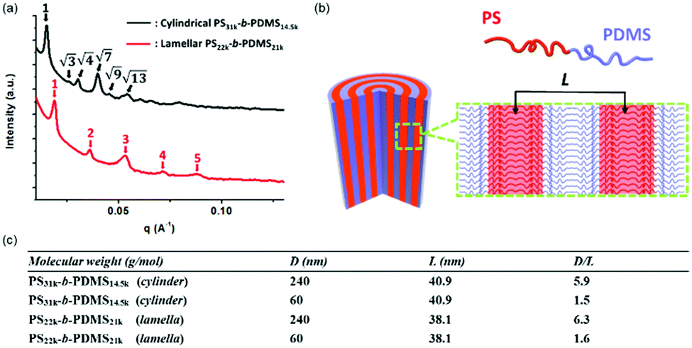 | ||
| Fig. 5 (a) Small angle X-ray scattering (SAXS) profiles of PS-b-PDMS in the bulk state with different compositions. The black and red lines represent the cylinder-forming (PS31k-b-PDMS14.5k) and the lamella-forming (PS22k-b-PDMS21k) samples, respectively. (b) Schematic illustration of lamella-forming PS-b-PDMS nanorods and the magnified lamellar structures, demonstrating the repeating period (L) of the block copolymer. (c) Table of the structural frustration factors (D/L) with different repeating periods (L) of the block copolymers and pore diameters (D) of the AAO templates. | ||
The structural frustration factors (D/L) are summarized in Fig. 5c. When commercial AAO templates are used (pore diameter ∼ 240 nm), the D/L values of cylinder-forming and lamella-forming PS-b-PDMS are ∼5.9 and ∼6.3, respectively, indicating that there should be about six repeating periods along the cross-sections of the nanostructures. The predictions are agreeable with our experimental results.
When synthesized AAO templates are used (pore diameter ∼60 nm), the D/L values of cylinder-forming and lamella-forming PS-b-PDMS decrease to ∼1.5 and ∼1.6, respectively, indicating that there should be only one or two repeating periods along the cross-sections of the nanostructures because of the smaller pore diameters. For the experimental data by confining lamella-forming PS-b-PDMS in the smaller nanopores (Fig. 4d), only two repeating periods are observed, which agrees with our calculated predictions. For the confinement with even lower D/L values, single periods in the nanostructures are expected.39
Conclusions
In this work, we discover that PS-b-PDMS can be infiltrated into the nanopores of AAO templates via a microwave-annealing-induced wetting process. By changing the compositions of the block copolymers, various morphologies such as parallel cylindrical morphology and concentric lamellar morphology can be obtained. Moreover, nanostructures with specific internal morphologies can be controlled using synthesized AAO templates with smaller pore diameters. The morphologies can be controlled by tuning the commensurabilities between the pore diameters of the AAO templates and the repeating periods of PS-b-PDMS. In the future, we will incorporate block copolymers with inorganic or metal nanoparticles to investigate the effect of microwave annealing on the morphologies of the hybrid materials, a promising direction to prepare block copolymer nanostructures with controlled morphologies and funtionalities.Experimental section
Materials
Poly(styrene-block-dimethylsiloxane) copolymers were obtained from Polymer Source. The polydispersity index (PDI) for the copolymers with the number-average molecular weights of (31-b-14.5) and (22-b-21) kg mol−1 were 1.15 and 1.08, respectively. Toluene was purchased from Tedia. Acetone and isopropyl alcohol were obtained from Echo Chemical. Ammonium hydroxide (NH4OH) was purchased from J. T. Baker. Deionized water was obtained from a Milli-Q system. Hydrogen fluoride (HF) was purchased from Union Chemicals. Porous anodic aluminum oxide (AAO) templates (pore diameter ∼150–400 nm, thickness ∼60 μm) were purchased from Whatman. Polycarbonate filters (VCTP, pore size ∼0.1 μm) were obtained from Millipore. Four-inch Si (1 0 0) wafers were purchased from Guv Team International.Preparation of synthesized AAO templates
The synthesized AAO templates were fabricated using a two-step anodization process.21,22 First, acetone was used to degrease a high-purity aluminum sheet (99.99%, 0.5 mm thick). After being rinsed with isopropyl alcohol (IPA), the aluminum sheet was electropolished in a mixed solution of perchloric acid/ethanol (v/v = 20/80) at 4 °C. The first anodization process was conducted at 40 V in 0.3 M oxalic acid at 4 °C for 2 h. The resultant aluminum oxide film was then chemically etched in a mixed solution of 1.8 wt% potassium dichromate (K2Cr2O7) and 6 wt% phosphoric acid (H3PO4) for 1 h. The second anodization process was conducted under the same conditions as for the first anodization process for different lengths of time. Finally, the template was further pore-widened in 5 wt% phosphoric acid at 30 °C for 40 min and the average pore diameter was increased to ∼60 nm.Fabrication of PS-b-PDMS nanostructures
A silicon wafer was cleaned by isopropyl alcohol and acetone in ultrasonication. The wafer was then rinsed by water and purged by N2 to remove the residual solvent. Subsequently, a 1 wt% PS-b-PDMS/toluene solution (50 μL) was dropped on the wafer, forming the PS-b-PDMS film after solvent evaporation. A porous AAO template was then placed on top of the polymer thin film. Later, the sample was moved to a microwave synthesizer (CEM discover Benchmate) to conduct the microwave-annealing-induced nanowetting process. The sample was irradiated at 190 °C for 15 min. A frequency of 2.45 GHz with a power of 15 W was applied to reach the annealing temperature. An in-built infrared detector was used to control the microwave heating power during the annealing processes. After the sample was taken out of the chamber and cooled to room temperature, the template was selectively removed by NH4OH(aq), releasing the block copolymer nanostructures.Selective removal of PDMS in the PS-b-PDMS nanostructures
The selective removal processes were used to confirm the spatial distribution of the PS domain in the nanostructures. After the sample was filtered by a polycarbonate membrane, a 48 wt% HF solution (2 mL) was dropped onto the nanostructure-containing membrane to remove the PDMS part of the PS-b-PDMS nanostructures.Structure analysis and characterization
The surface morphologies of the block polymer nanostructures were characterized using a JEOL JSM-7401F model scanning electron microscope (SEM) operating at an acceleration voltage of 5 kV. The samples were dried by a vacuum pump and coated with 4 nm of platinum before the SEM measurements. A bright-field transmission electron microscope (TEM) (JEOL JEM-2100) was also used to examine the internal morphologies of the block polymer nanostructures at an acceleration voltage of 200 kV. For TEM measurements, the samples were placed onto copper grids coated with a thin layer of Formvar. The small angle X-ray scattering (SAXS) experiments were conducted to determine the repeating periods of PS-b-PDMS in the bulk state at the beamline BL23A of the National Synchrotron Radiation Research Center (NSRRC). The beam conditions were fixed at a diameter of 0.5 mm, an energy of 10 keV, and a wavelength of 1.24 Å. PS-b-PDMS powders were measured at ambient temperature and sealed with two thin Kapton windows.Conflicts of interest
There are no conflicts to declare.Acknowledgements
This work was supported by the Ministry of Science and Technology of the Republic of China (Grant number: MOST 104-2628-E-009-008-MY3). We thank Dr. U-Ser Jeng and Dr. Chun-Jen Shu of the National Synchrotron Radiation Research Center (NSRRC) for their assistance in conducting the SAXS experiments.Notes and references
- F. S. Bates, Science, 1991, 251, 898–905 CrossRef CAS PubMed.
- I. W. Hamley, The Physics of Block Copolymers, Oxford University Press, New York, 1998 Search PubMed.
- F. S. Bates and G. H. Fredrickson, Phys. Today, 1999, 52, 32–38 CrossRef CAS.
- J. T. Chen and C. S. Hsu, Polym. Chem., 2011, 2, 2707–2722 RSC.
- M. C. Orilall and U. Wiesner, Chem. Soc. Rev., 2011, 40, 520–535 RSC.
- Y. S. Jung, W. Jung, H. L. Tuller and C. A. Ross, Nano Lett., 2008, 8, 3776–3780 CrossRef CAS PubMed.
- C. Liu, H. Qin and P. T. Mather, J. Mater. Chem., 2007, 17, 1543–1558 RSC.
- M. Park, C. Harrison, P. M. Chaikin, R. A. Register and D. H. Adamson, Science, 1997, 276, 1401–1404 CrossRef CAS.
- W. H. Li and M. Muller, Prog. Polym. Sci., 2016, 54-55, 47–75 CrossRef CAS.
- R. A. Segalman, Mater. Sci. Eng., R, 2005, 48, 191–226 CrossRef.
- Y. S. Jung and C. A. Ross, Adv. Mater., 2009, 21, 2540–2545 CrossRef CAS.
- C. Sinturel, M. Vayer, M. Morris and M. A. Hillmyer, Macromolecules, 2013, 46, 5399–5415 CrossRef CAS.
- S. S. Dinachali, W. B. Bai, K. H. Tu, H. K. Choi, J. S. Zhang, M. E. Kreider, L. C. Cheng and C. A. Ross, ACS Macro Lett., 2015, 4, 500–504 CrossRef CAS.
- X. J. Zhang, K. D. Harris, N. L. Y. Wu, J. N. Murphy and J. M. Buriak, ACS Nano, 2010, 4, 7021–7029 CrossRef CAS PubMed.
- C. Jin, J. N. Murphy, K. D. Harris and J. M. Buriak, ACS Nano, 2014, 8, 3979–3991 CrossRef CAS PubMed.
- X. J. Zhang, J. N. Murphy, N. L. Y. Wu, K. D. Harris and J. M. Buriak, Macromolecules, 2011, 44, 9752–9757 CrossRef CAS.
- D. Borah, M. T. Shaw, J. D. Holmes and M. A. Morris, ACS Appl. Mater. Interfaces, 2013, 5, 2004–2012 CAS.
- D. Borah, R. Senthamaraikannan, S. Rasappa, B. Kosmala, J. D. Holmes and M. A. Morris, ACS Nano, 2013, 7, 6583–6596 CrossRef CAS PubMed.
- C. R. Martin, Science, 1994, 266, 1961–1966 CAS.
- C. R. Martin, Acc. Chem. Res., 1995, 28, 61–68 CrossRef CAS.
- H. Masuda and K. Fukuda, Science, 1995, 268, 1466–1468 CAS.
- H. Masuda, H. Yamada, M. Satoh, H. Asoh, M. Nakao and T. Tamamura, Appl. Phys. Lett., 1997, 71, 2770–2772 CrossRef CAS.
- A. P. Li, F. Muller, A. Birner, K. Nielsch and U. Gosele, J. Appl. Phys., 1998, 84, 6023–6026 CrossRef CAS.
- J. Martin, J. Maiz, J. Sacristan and C. Mijangos, Polymer, 2012, 53, 1149–1166 CrossRef CAS.
- K. Shin, H. Xiang, S. Moon, J. K. Kim, T. J. McCarthy and T. P. Russell, Science, 2004, 306, 76 CrossRef CAS PubMed.
- A. C. Shi and B. H. Li, Soft Matter, 2013, 9, 1398–1413 RSC.
- Y. M. Sun, M. Steinhart, D. Zschech, R. Adhikari, G. H. Michler and U. Gosele, Macromol. Rapid Commun., 2005, 26, 369–375 CrossRef CAS.
- H. Q. Xiang, K. Shin, T. Kim, S. I. Moon, T. J. McCarthy and T. P. Russell, Macromolecules, 2004, 37, 5660–5664 CrossRef CAS.
- H. Xiang, K. Shin, T. Kim, S. I. Moon, T. J. McCarthy and T. P. Russell, Macromolecules, 2005, 38, 1055–1056 CrossRef CAS.
- H. Q. Xiang, K. Shin, T. Kim, S. Moon, T. J. McCarthy and T. P. Russell, J. Polym. Sci., Part B: Polym. Phys., 2005, 43, 3377–3383 CrossRef CAS.
- P. Dobriyal, H. Q. Xiang, M. Kazuyuki, J. T. Chen, H. Jinnai and T. P. Russell, Macromolecules, 2009, 42, 9082–9088 CrossRef CAS.
- S. L. Mei, L. Wang, X. D. Feng and Z. X. Jin, Langmuir, 2013, 29, 4640–4646 CrossRef CAS PubMed.
- C. J. Chu, P. Y. Chung, M. H. Chi, Y. H. Kao and J. T. Chen, Macromol. Rapid Commun., 2014, 35, 1598–1605 CrossRef CAS PubMed.
- C. W. Chang, M. H. Chi, C. W. Chu, H. W. Ko, Y. H. Tu, C. C. Tsai and J. T. Chen, RSC Adv., 2015, 5, 27443–27448 RSC.
- Y. S. Jung and C. A. Ross, Nano Lett., 2007, 7, 2046–2050 CrossRef CAS PubMed.
- K. W. Gotrik, A. F. Hannon, J. G. Son, B. Keller, A. Alexander-Katz and C. A. Ross, ACS Nano, 2012, 6, 8052–8059 CrossRef CAS PubMed.
- J. B. Chang, J. G. Son, A. F. Hannon, A. Alexander-Katz, C. A. Ross and K. K. Berggren, ACS Nano, 2012, 6, 2071–2077 CrossRef CAS PubMed.
- M. F. Zhang, P. Dobriyal, J. T. Chen, T. P. Russell, J. Olmo and A. Merry, Nano Lett., 2006, 6, 1075–1079 CrossRef CAS.
- B. Yu, P. C. Sun, T. H. Chen, Q. H. Jin, D. T. Ding, B. H. Li and A. C. Shi, J. Chem. Phys., 2007, 127, 114906 CrossRef PubMed.
Footnote |
| † Electronic supplementary information (ESI) available: SEM images of the AAO templates, heating profiles and polymer nanostructures. See DOI: 10.1039/c7sm02103h |
| This journal is © The Royal Society of Chemistry 2018 |