
 Open Access Article
 This Open Access Article is licensed under a
 Creative Commons Attribution 3.0 Unported Licence
Candidate photoferroic absorber materials for thin-film solar cells from naturally occurring minerals: enargite, stephanite, and bournonite†
Suzanne K.
Wallace
 ab,
Katrine L.
Svane
a,
William P.
Huhn
c,
Tong
Zhu
c,
David B.
Mitzi
cd,
Volker
Blum
cd and
Aron
Walsh
*be
ab,
Katrine L.
Svane
a,
William P.
Huhn
c,
Tong
Zhu
c,
David B.
Mitzi
cd,
Volker
Blum
cd and
Aron
Walsh
*be
aDepartment of Chemistry, Centre for Sustainable Chemical Technologies, University of Bath, Claverton Down, Bath, BA2 7AY, UK
bDepartment of Materials, Imperial College London, Exhibition Road, London SW7 2AZ, UK. E-mail: a.walsh@imperial.ac.uk
cDepartment of Mechanical Engineering and Materials Science, Duke University, Durham, North Carolina 27708, USA
dDepartment of Chemistry, Duke University, Durham, North Carolina 27708, USA
eGlobal E3 Institute, Department of Materials Science and Engineering, Yonsei University, Seoul 03722, Korea
First published on 28th June 2017
Abstract
To build on the success of other mineral systems employed in solar cells, including kesterites (Cu2ZnSnS4) and herzenbergite (SnS), as well as mineral-inspired systems such as lead halide perovskites (CH3NH3PbI3), we have searched for photoactive minerals with the additional constraint that a polar crystal structure is adopted. Macroscopic electric fields provide a driving force to separate electrons and holes in semiconductor devices, while spontaneous lattice polarisation in polar semiconductors can facilitate microscopic photo-carrier separation to enhance carrier stability and lifetimes. We identify enargite (Cu3AsS4), stephanite (Ag5SbS4), and bournonite (CuPbSbS3) as candidate materials and explore their chemical bonding and physical properties using a first-principles quantum mechanical approach.
1 Introduction
A key component of the pathway towards terawatt-scale solar power generation is the continued reduction in cost, whilst also improving the performance of solar modules.1 The search for candidate ‘thin-film’ photovoltaic (PV) materials that are able to absorb sunlight more strongly than silicon is an active area of research to enable the fabrication of cost-effective and highly-efficient solar cell devices.2 Common ways to screen for such materials include looking for systems with an optical band gap that is direct and well-matched to the solar spectrum3 and with an abrupt onset in the absorption spectrum.4Interest in this field has intensified in recent years with the remarkable power conversion efficiencies (PCEs) achieved with lead halide perovskites. PCEs of around 20% (ref. 5 and 6) have been achieved over a much shorter period of development than has been needed for many other PV technologies to achieve the same level of performance.7 Lead halide perovskites currently out-perform many other materials that also meet the aforementioned screening criteria, such as Cu2ZnSn(S,Se)4 (ref. 8) and SnS.9 Of this class of materials, methylammonium lead iodide (CH3NH3PbI3 or MAPbI3) particularly stands out for its champion device efficiencies.6
The long minority-carrier lifetimes of 280 ns (ref. 10) and diffusion lengths up to 175 microns (ref. 11) demonstrated by MAPbI3-based devices are comparable with the best single-crystal semiconductors,12 even with low-cost solution processing fabrication methods from which one would usually expect to produce a lower-quality defective material. In contrast, other candidate thin-film PV materials such as Cu2ZnSn(S,Se)4 (ref. 8) and SnS9 suffer from short minority carrier lifetimes and diffusion lengths and, ultimately, large open-circuit voltage deficits in photovoltaic devices. The difference in behaviour can be attributed to ‘defect tolerance’. Either the formation of detrimental defects are avoided (e.g. due to high formation energies) or their effects are minimised (due to their shallow nature within the band gap or to effective dielectric screening). It has also been suggested that the presence of polar domains in MAPbI3 could contribute to the low recombination rate (and hence long carrier lifetimes) due to the enhanced spatial separation of carriers.13 The presence of macroscopic ferroelectricity in hybrid perovskites remains a matter of research and debate, but there is growing evidence supporting polar domains at room temperature.14–16
In this study we consider only naturally occurring minerals, and so one could expect that the materials would not suffer from the same instability issues observed for lead halide perovskites.17 We start from a small dataset18 of ∼200 known, naturally occurring minerals and aim to identify materials that possess many of the desirable properties for an efficient material for solar energy conversion, using screening criteria discussed in the next section. We then investigate the chemical and physical properties of three candidate systems using a first-principles quantum mechanical approach to assess if these materials are likely to be capable of producing efficient photovoltaic devices.
2 Search for light absorbing polar minerals
2.1 Mineral screening criteria
Our screening criteria is outlined in the Venn diagram shown in Fig. 1 and the rationale behind our screening procedure is outlined below. The candidate materials we identified from a dataset of 193 naturally occurring multi-component minerals18 are those that could both absorb light within the energy range that makes up the majority of the solar spectrum and possibly exhibit ferroelectricity. The combination of light absorption, semiconductivity, and ferroelectricity in a single material can give rise to novel photoferroic effects.19 | ||
| Fig. 1 Venn diagram outlining our screening criteria used to extract candidate photoferroic materials from a sample of 193 naturally occurring minerals, which we could expect to be thermodynamically stable compounds. A mineral with a dark streak colour suggests that it will possess a band gap within the energy range of visible light. Similarly, a polar crystal structure is a necessary, but not sufficient, condition for a material to exhibit ferroelectricity. | ||
The most fundamental property to consider for an efficient PV material is an optical band gap that is direct with a magnitude within a range that is well-matched to the solar spectrum. The optimal energy range for the optical band gap of single-junction solar cells is approximately 1.0 to 1.7 eV.20 The streak colour of a mineral can be indicative of visible light absorption. The streak colour is that of the crushed powder, usually identified by producing a streak across a porcelain tile. While the observed colour of a mineral in massive form can vary considerably between different samples, the colour of the streak remains consistent. A mineral with a dark streak colour implies, but does not guarantee, that it will possess a band gap within the optimal range for the absorption of sunlight. We obtained information on the streak colour of the minerals from ref. 18 and this formed our first screening criterion, reducing the dataset from 193 to 36 minerals.
Our second screening criterion is the potential to exhibit ferroelectricity. A ferroelectric material is one that exhibits a spontaneous electric dipole moment within the unit cell, and so this is present even without the application of an electric field, but the direction of polarisation can be changed when an external electric field is applied. To identify candidate ferroelectric materials, we screen the space groups of materials to search for those that adopt crystal structures with a polar point group. This screening criterion then limited our dataset from 36 to 4. However, we discounted ZnS from our study because it is known to be a wide band gap semiconductor when prepared in pure form.
A polar point group is a necessary but not sufficient property for a material to exhibit ferroelectricity and so acts as a good starting point for further study of the materials. Desirable effects could be obtained with local polarisation alone, once the correlation length of spontaneous polarisation is sufficient to interact with electron and hole carriers (typically tens of nm). Furthermore, polar structures lack a centre of inversion symmetry and so they are not bound by the same optical selection rules, which could reduce the likelihood of dipole-disallowed transitions21 and the associated reduction in the strength of the onset of absorption for direct gap materials as outlined by Yu and Zunger in their spectroscopically limited maximum efficiency (SLME) metric.4
2.2 Photoferroics for PV devices
Ferroelectric materials typically display large dielectric constants due to low-energy polarisation mechanisms.22 This can have a number of implications for carrier transport and lifetimes in PV materials, such as a reduction in the electrostatic force between an electron–hole pair (low exciton binding energies), potentially leading to a reduced rate of electron–hole recombination in the material,23 provided the nuclear subsystem is able to respond on a fast enough time scale. Also, the capture cross-section for charge carriers by a charged defect can be reduced by the charge screening in a dielectric material, possibly allowing for more defect-tolerant carrier transport.12In addition to the desirable properties that could be expected for ferroelectric materials, there are a number of novel phenomena that have been observed in photoactive polar semiconductors that are outlined in ref. 24, which could open up new pathways to highly efficient PV devices. The potential of utilising ferroelectric crystals for solar cells was first highlighted in the work of V. M. Fridkin,25,26 but the observation of novel photovoltaic phenomena in polar crystals dates back even earlier. The bulk photovoltaic effect (BPE) was first recorded in 1956 in BaTiO3,27 where photovoltages were measured in un-doped single crystals.24 The BPE effect is distinct from the typical PV effect in a solar cell where the electric fields that drive photo-carrier separation are typically associated with a ‘p–n’ or ‘p–i–n’ junction. In the BPE it is the internal electric fields arising from spontaneous polarisation of the lattice that drive the photocurrent. It is therefore possible for charge-carrier generation and separation to occur simultaneously in the bulk material. It has recently been demonstrated experimentally in ferroelectric single crystals of BaTiO3 that electron–hole recombination is inhibited by the presence of the internal fields, with recombination being rapidly accelerated after the ferroelectric dipole was switched off.28
The anomalous photovoltaic effect (APE) was first observed in PbS films in 1946 (ref. 29) and has since been reported in polycrystalline CdTe, ZnTe and InP,30–32 where photovoltages output along the polarisation direction can be significantly larger than the band gap of the material,33 which is usually the upper limit for a semiconductor PV material.24 The Shockley–Queisser limit,3 which prevents any single p–n junction solar cell from converting more than one third of the incident light into electricity, can in principle be surpassed by exploiting such phenomena.34
Most of the commonly studied ferroelectric materials such as LiNbO3 and BaTiO3 have band gaps larger than 3 eV and can therefore only absorb sunlight in the UV range, which accounts for only around 3.5% of the solar spectrum.33 The efficiency of PV devices made from these materials is therefore severely limited by the large band gaps. Research efforts have gone into adjusting the optical absorption of ferroelectric materials without influencing the ferroelectric properties of the material through chemical doping or alloying.33 In Bi3Ti3O12 the optical band gap has been tuned in such a way, resulting in a decrease from 3.6 eV to 2.7 eV,35 although this is still considerably larger than the optimal range for a PV absorber material. There are some known ferroelectric materials with band gaps closer to the optimal range. Ferroelectricity in SbSI was studied extensively in the 1960's and has a value of approximately 2 eV for the band gap, which can be tuned by varying the chalcogen and halide.36 The Curie temperature for the phase transition from a polar to paraelectric phase for this material has been measured to be around room temperature.37 With typical operating temperatures of solar cell devices approaching 50 °C,38 it could prove difficult to exploit the ferroelectricity of this material in a working device. As the set of materials we screened are all naturally-occurring minerals with polar structures, they may retain their polar crystal structure under typical operating conditions of a solar cell.
2.3 Candidate minerals
From our screening process, we identified three sulfosalt minerals: enargite (Cu3AsS4), stephanite (Ag5SbS4), and bournonite (CuPbSbS3), which are shown in Fig. 2. A basic sulfosalt mineral can be defined as a ternary compound AxByCz, which is the case for enargite (Cu3AsS4) and stephanite (Ag5SbS4). Options for species A include: Cu, Ag, Pb, Sn, Mn, amongst others. Species B can be either: As, Sb or Bi. Options for species C includes: S, Se and Te. It is also possible to form quaternary sulfosalt compounds from isoelectronic substitution of additional transition metals, as in the case of bournonite (CuPbSbS3). The occurrence of these materials in nature under ambient conditions indicates thermodynamic stability.39 Although these materials are naturally occurring minerals, knowledge of their optoelectronic properties is scarce. | ||
| Fig. 2 Illustrations of the crystal structures of candidate solar minerals: enargite (space group Pmn21), stephanite (space group Cmc21), and bournonite (space group Pmn21). | ||
A very recent experimental study assessed the band gaps and photovoltaic response of six sulfide minerals, which included the three sulfosalt minerals we investigate in this study.40 However, the potential of sulfosalt minerals for PV applications was first highlighted by Dittrich et al. in 2007.39 This work and ref. 41 provide overviews of crystal growth and thin-film deposition methods that have been developed for synthesising sulfosalt layers. There are works in the literature referring to synthetic samples of enargite42 and stephanite.43 A recent study on bournonite44 also details a procedure for synthesising this material.
The possibility of using low temperature thin-film deposition conditions for sulfosalt solar cells has been highlighted.39 Such an approach could enable the use of a wide variety of substrates or to reduce the interaction with the back contact during deposition, which is believed to be detrimental in Cu2ZnSnS4 devices with the Mo back contact reacting with the absorber layer to form MoS2.45 However, it is worth noting that the mineral class of ‘sulfosalts’ contains materials with a diverse range of crystal structures; therefore the extent of the similarity of physical properties of different sulfosalt materials is not clear.
3 Computational details
3.1 Density functional theory
The electronic structure of the three candidate photoferroic materials was calculated using the FHI-aims46–48 all-electron electronic structure code, which is an implementation of density functional theory (DFT) based on numeric atom-centered orbital basis sets with a linear-scaling approach to hybrid functionals.49,50 We use the short-range screened hybrid exchange–correlation HSE06 functional51 and spin–orbit coupling (SOC)52 is included. Hybrid DFT functionals have been found to correct for the underestimation of the optical band gap inherent in the generalized gradient and local density approximations.53,54The FHI-aims default ‘tight’ numerical settings are used for all calculations, which specifies the basis sets, integration grids, and Hartree potential. Structural optimization was performed with the Broyden–Fletcher–Goldfarb–Shanno algorithm. We fix the lattice parameters of the unit cell to room temperature X-ray diffraction data values from the Inorganic Crystal Structure Database (ICSD)55 and optimize the internal coordinates with a tolerance of 10−3 eV Å−1. A Γ-centred 4 × 4 × 4 k-point grid is used to sample the electronic Brillouin zone for structural optimization, but a more dense k-point grid of 8 × 8 × 8 was required for convergence for band structure calculations. Convergence tests for the calculation settings are given in the ESI.† All visuals of atomic and electronic structure are produced using VESTA.56
3.2 Carrier effective masses
To assess the semiconducting potential of these materials, we obtain values for the carrier effective masses (m*) at the band extrema of the electronic band structures. We use a fitting procedure for the three independent components of the m* tensor for an orthorhombic crystal structure, shown in eqn (1), where the three components are in three directions parallel to crystallographic directions a, b and c (∥a, ∥b and ∥c), respectively. | (1) |
Once the location of the band extrema has been determined from our calculated electronic band structures, we recalculate the band structure over a restricted data range close to the band extrema along the three axes. We then obtain expressions for the three components of m* at the upper valence and lower conduction bands by numerical parabolic fits to the calculated restricted band structures within a fitting range of k0 ± 0.01 bohr−1, using eqn (2), where k0 denotes the location of the band extremum in k-space.
 | (2) |
3.3 Optical response function
The linear macroscopic dielectric tensor as a function of photon frequency, εij(ω), of each material is calculated within the random phase approximation as implemented in FHI-aims, following the derivation in ref. 57. We use this to predict the high-frequency dielectric response of the semiconductor to incident sunlight, i.e. the response of the electron density. Inter- and intra-band contributions to the dielectric function are computed, but the former dominate the optical spectra of semiconducting materials. Indirect (phonon assisted) transitions are not accounted for, and generally have weaker intensity, but may make a substantial contribution to the optical properties of materials with strongly indirect band structures.A k-point grid of 8 × 8 × 8 was required to reach convergence in the calculated dielectric function for bournonite (CuPbSbS3), whereas a more dense k-point grid of 10 × 10 × 10 was required for both enargite (Cu3AsS4) and stephanite (Ag5SbS4). Data for convergence tests are included in the ESI.†
We obtain the frequency-dependent absorption coefficient in units of cm−1 for each material from the real and imaginary components of the dielectric function using eqn (3). The derivation for the units of the absorption coefficient is given in the ESI.†
 | (3) |
3.4 Spontaneous polarisation
To investigate the strength of polarity, calculations of the spontaneous electric polarisation, Ps, of each material were performed using the Berry-phase formalism58 with the methodology outlined in ref. 59. Only differences in polarisation are physically meaningful; we therefore optimise the structure with polarisation +Ps and invert this structure to get the opposite polarisation, −Ps. The polarisation difference between those two structures, 2Ps, is calculated. We verify that the change in polarisation is continuous by considering the polarisation for a number of configurations connecting the two structures, with their coordinates r obtained from eqn (4), where λ is a number between 0 and 1.| r = λrPs + (1 − λ)r−Ps | (4) |
These calculations were performed in VASP60,61 using the HSE06 functional,51 projector augmented wave core potentials62 and a 500 eV plane wave cutoff energy, without including SOC. Sampling of the electronic Brillouin zone using a 2 × 2 × 2 grid of k-points was found to be converged with respect to the calculated polarisation values. Further details of the polarisation calculations are included in the ESI.†
4 Results and discussion
In the following sections we assess the predicted optoelectronic properties of each material in turn. As discussed in the introduction, an effective PV material must absorb light and transport charge. In addition to the band gap and carrier effective masses, we consider the dielectric function, and the associated optical absorption spectra. We finish with an assessment of spontaneous electric polarisation to determine the strength of the polarity in the materials and the effect on the electronic band structure.4.1 Enargite (Cu3AsS4)
The potential of the sulfosalt mineral enargite (Cu3AsS4) for PV applications was suggested by Pauporté and Lincot in 1995.42 It received little scientific interest until Yu and Zunger's high-throughput study based on their SLME metric, where they calculate a theoretical power conversion efficiency of 25.5% for the material.4 A recent experimental work has emerged assessing the photovoltaic response of six minerals, including enargite.40The crystallographic unit cell (as shown in Fig. 2) has orthorhombic symmetry with space group Pmn21 and tetrahedral coordination for all atoms.63 It has recently been proposed that tetrahedrally bonded multinary semiconductors may be more prone to cation disorder, and the associated extended antisite defect pairs, than lower dimensional multinary compounds.64 However, compared to materials such as Cu2ZnSn(S,Se)4 that are known to suffer from mixing of Cu and Zn cations,65–67 the cations in enargite are more dissimilar in terms of charge and radius. It has been shown that replacing cations with species further apart on the periodic table can reduce this type of disorder.68–71 We therefore expect cation disorder to be reduced in this compound, as has been found to be the case when substituting Cu with Ag70 or Zn with Ba68,69 in Cu2ZnSn(S,Se)4.
Enargite is a mineral semiconductor of type AI3BVCII4. Natural samples of enargite are frequently found as an impurity in copper ores.72 Natural samples have been found to exhibit the electrical properties of a p-type doped semiconductor with a conductivity of 0.0014 S m−1 (from the stated value of approximately 7 Ω cm for the resistivity at 295 K).42 The main impurities in natural enargite are Sb and Fe, but Pb and Ag are also known to be present.72 In a recent study on natural sulfide minerals,40 the authors detected <1% of Sb impurities in the natural samples of enargite, which show a clear p-type photoconductivity. The p-type response could either be due to intrinsic acceptor defects or due to defects introduced by the Sb impurities. In 1995, Pauporté and Lincot measured two optical transitions in enargite: an indirect one at 1.19 eV and a direct one at 1.44 eV. However more recent studies have reported values of 1.28 eV (ref. 41) and 1.36 eV (ref. 40) for a direct band gap, with some photocurrent due to band tailing further in the IR region for the latter, which the authors attribute to lattice disorder or impurity states in the band gap. G0W0 calculations based on wavefunctions generated from the hybrid functional HSE06 (ref. 51) predicted a value of 1.32 eV for the band gap.73 Although a number of different values have been reported for the band gap of enargite, all values fit within the optimal range for a solar absorber material.20
For enargite, we predict a direct band gap at the Γ point with a magnitude of 1.24 eV, which is close to the reported G0W0@HSE06 value of 1.32 eV.73 The calculated band structure is shown in Fig. 3a. The conduction band minimum (CBM) is dispersive, indicating the potential for high carrier mobility at the band edge. This is confirmed by the estimates for the minority carrier effective masses of electrons in the conduction band, mc, presented in Table 1, which also indicates that the effective masses from Γ → X, Y, Z are almost isotropic. However, the estimated values for effective masses in Table 1 indicate that holes are heavier along the Γ → Y, Z directions in enargite.
 | ||
| Fig. 3 Calculated electronic band structure of enargite (Cu3AsS4) (a) and the reciprocal space k-path for the structure determined by the Aflow-online utility74 (b). | ||
| Enargite (Cu3AsS4) | Stephanite (Ag5SbS4) | Bournonite (CuPbSbS3) | ||||||||||||
|---|---|---|---|---|---|---|---|---|---|---|---|---|---|---|
| Direction | m e | m h | ε | Direction | m e | m h | ε | Direction | m e | m h | ε | |||
| ∥a | 0.20 | 0.22 | ε ∞ xx | 5.70 | ∥a | 0.37 | 0.60 | ε ∞ xx | 6.01 | ∥a | 0.52 | 0.99 | ε ∞ xx | 7.16 |
| ∥b | 0.23 | 1.20 | ε ∞ yy | 5.89 | ∥b | 0.40 | 1.94 | ε ∞ yy | 5.86 | ∥b | 0.37 | 0.97 | ε ∞ yy | 7.24 |
| ∥c | 0.22 | 1.35 | ε ∞ zz | 5.91 | ∥c | 0.26 | 0.77 | ε ∞ zz | 5.83 | ∥c | 0.50 | 0.86 | ε ∞ zz | 7.55 |
It has been suggested for other semiconducting materials that the defect-tolerance of optoelectronic properties, to a certain extent, can be associated with an electronic structure where the VBM possesses predominantly antibonding character.12,77,78 CuInSe2 is an example of another thin-film PV technology that is defect tolerant with shallow defects78 and benign grain boundaries.79,80 The electronic density of states (DOS) at the top of the valence band in enargite, which is shown in Fig. 4, shares some common features with that of CuInSe2. In the case of CuInSe2 the upper valence bands consist of the hybridized Cu d-states and Se p-states, whereas for enargite it is instead S p-states hybridized with Cu d-states. The p–d repulsion is large in CuInSe2 and appears to be even larger in enargite. In CuInSe2, the p–d repulsion gap separates the bonding p–d states below and the antibonding p–d states above, yielding antibonding states for the upper valence bands.
 | ||
| Fig. 4 HSE06 + SOC partial electronic density of states (pDOS) of enargite (Cu3AsS4), where the top of the valence band has been set to 0 eV. | ||
To assess further if enargite possesses an upper valence band with antibonding character we visualize the electron wavefunction of the highest occupied state, as is shown in Fig. 5a. From this, the opposite parity of neighbouring S p-orbitals and Cu d-orbitals indicates antibonding character at the valence band maximum, which could suggest that acceptor defects are more likely to produce shallow defect levels with respect to the band edges. Enargite may therefore have defect-tolerant optoelectronic properties, which has been suggested in some recent studies. Firstly, the photocurrent conversion efficiency of a natural enargite sample was found to be greater than that of a natural kesterite sample.40 Secondly, the photocurrent density measured for enargite nanocrystals had a 10-fold improvement to that of Cu3SbS4 nanocrystals,81 both of which could be expected to possess highly-defective nanocrystalline structures.
 | ||
| Fig. 5 The real component of the electron wavefunction of the highest occupied state in (left panel) enargite (Cu3AsS4), (centre panel) stephanite (Ag5SbS4) and (right panel) bournonite (CuPbSbS3), showing sulfur p-orbitals and copper d-orbital in enargite and bournonite and silver d-orbitals in stephanite. The difference in colour indicates the different parity of the wavefunctions and the position of the ions are indicated on the plot. | ||
 | ||
| Fig. 6 Three independent components of the calculated optical dielectric tensor, ε(ω), as a function of incident photon energy, ω, for enargite (Cu3AsS4). | ||
In Fig. 7 we plot the isotropic average of the optical absorption coefficient, α(ω), of enargite, with comparison to GaAs and MAPbI3, as known strong PV absorber materials, and crystalline Si (c-Si) as a material that is known to have weak absorption. Enargite has a comparable strength of absorption to the strong absorber materials GaAs and MAPbI3, and considerably stronger than c-Si, within the region for the onset of absorption (incident photon energy of approximately ω = 1–3 eV).
 | ||
| Fig. 7 Isotropic average of the optical absorption coefficient for three sulfosalt materials enargite (Cu3AsS4), stephanite (Ag5SbS4) and bournonite (CuPbSbS3) plotted in comparison to the same parameter for other important photovoltaic materials over the onset energy range (1–3 eV). The comparison photovoltaic materials include: the strong direct-gap absorber material GaAs, the weaker indirect-gap absorber crystalline-Si and the hybrid perovskite MAPbI3, where data for these latter compounds was taken from ref. 82. | ||
4.2 Stephanite (Ag5SbS4)
The unit cell of the second candidate, stephanite (Ag5SbS4), also has an orthorhombic crystal structure but with space group Cmc21 (Fig. 2). The chemical formula suggests formal oxidations states of Ag(I) and Sb(III), which are associated with 4d10 and 5s2 valence electronic configurations. The structure consists of SbS3 trigonal pyramids layered along the c-axis that are connected with Ag atoms that form triangular and near tetrahedral structures with S atoms.40 As was discussed for enargite, the components in stephanite are dissimilar in terms of charge and size, so it could be expected that cation disorder will not be prevalent in this compound.There is limited literature on the optical or electrical properties of stephanite apart from a work in 1973 (ref. 43) showing the electrical resistivity of a synthetic sample of stephanite as a function of temperature. They report a resistivity of approximately 9 Ω cm at 110 °C, which corresponds to a conductivity of 0.0011 S m−1. It has been reported that stephanite has a band gap of 1.62 eV (ref. 41) and a recent study on a natural sample of stephanite has measured a band gap of 1.67 eV and p-type conductivity.40 Chemical analysis indicated that there was no detectable level of impurities present.40 This could suggest that the p-type conductivity of the crystal is due to the presence of acceptor intrinsic defects in stephanite (e.g. VAg−). The work40 also comments on the possibility of high Ag ion conductivity. Ion transport has been suggested as a cause of current–voltage hysteresis in lead halide perovskites;84 but it can also contribute to ‘self-healing’ of detrimental extended defects as ions can redistribute over time.
There has been some speculation in the literature on the possibility of ferroelectric behaviour in stephanite due to the presence of polar phases at low temperatures in pyrargyrite (Ag3SbS3), proustite (Ag3AsS3), and stibnite (Sb2S3), which are crystallochemically related to stephanite.85 The same study notes that similar displacive structural changes occur in stephanite to those in proustite and pyrargyrite that are responsible for the ferroelectric properties.
 | ||
| Fig. 8 Calculated electronic band structure of stephanite (Ag5SbS4) (a) and the reciprocal space k-path for the structure determined by the Aflow-online utility74 (b). | ||
 | ||
| Fig. 9 HSE06 + SOC partial electronic density of states (pDOS) of stephanite (Ag5SbS4), where the top of the valence band has been set to 0 eV. | ||
 | ||
| Fig. 10 Three components of the calculated dielectric function, ε(ω), as a function of incident photon energy, ω, for stephanite (Ag5SbS4). | ||
4.3 Bournonite (CuPbSbS3)
Bournonite (CuPbSbS3) again adopts an orthorhombic crystal structure and the same space group as enargite, Pmn21. The unit cell of bournonite is shown in Fig. 2. The structure is derived from stibnite (Sb2S3), where Pb(II) atoms alternatively occupy the Sb(III) sites and Cu(I) atoms form tetrahedra to compensate for the charge.40Measured values of 1.23 eV (ref. 41) and 1.31 eV (ref. 86) have been reported for the band gap, which are both within the optimal range for a solar absorber material. Recently, this material has received increasing scientific interest for thermoelectric and rewriteable data storage applications due to a low thermal conductivity, which has been attributed to the distorted environments of the Pb(II) and Sb(III) atoms from the stereochemically active lone-pair s2 electrons.44 Consequently, works on the synthesis of bournonite are beginning to emerge.86 A study of two natural samples of bournonite40 reported n-type conductivity, a direct gap of 1.29 eV, and an indirect band gap of 1.17 eV in one sample, and the same direct band gap and a lower indirect band gap of 1.01 eV in another.
 | ||
| Fig. 11 Calculated band structure of bournonite (CuPbSbS3) showing the result without the inclusion of spin–orbit coupling (SOC) in green and the calculation including SOC in red (a) and the reciprocal space k-path for the structure determined by the Aflow-online utility74 (b). | ||
The upper valence band of bournonite is formed primarily of hybridized Cu d-states and S p-states (Fig. 12), although there does not appear to be a pronounced p–d repulsion as was shown in the pDOS plot for enargite. Contributions from Sb and Pb s-states at the VBM appear to be minor. In Fig. 5c we visualize the electron wavefunction of the highest occupied state in bournonite to determine the bonding characteristics. As for the previous two materials, the opposite parity of the electron wavefunctions for the anion and cation show antibonding character, which could support defect tolerance.
 | ||
| Fig. 12 HSE06 + SOC partial electronic density of states (pDOS) of bournonite (CuPbSbS3), where the top of the valence band has been set to 0 eV. | ||
 | ||
| Fig. 13 Three components of the calculated dielectric function, ε(ω), as a function of incident photon energy, ω, for bournonite (CuPbSbS3). | ||
4.4 Polarisation and Rashba splitting
The results presented above have shown the three candidate materials have electronic and optical properties suitable for solar energy harvesting. An additional criterion for our search is that the materials adopt a polar space group. | ||
| Fig. 14 Spontaneous polarisation along a path connecting the structures with +Ps and −Ps for enargite (Cu3AsS4), stephanite (Ag5SbS4) and bournonite (CuPbSbS3). The markers indicate points calculated with 2 × 2 × 2 k-points and the dashed line is the path obtained using 1 × 1 × 1 k-points. The curves are set to pass through 0 for λ = 0.5. See ESI† for further details. | ||
It is worth noting that for the materials in this study the switching from one polarisation to the other requires a significant rearrangement of the atoms. We estimate the switching barrier from the energy change along the paths used to calculate the spontaneous lattice polarisation, but note that this estimate is an upper limit for the switching barrier as the intermediate structures have not been relaxed to their minimum energy configuration (further details included in the ESI†). We estimate the upper limit for the switching barrier to be 19.7, 12.5 and 21.8 eV per unit cell for enargite, stephanite and bournonite; which are orders of magnitude larger than barriers calculated for BaTiO3.89 Thus, the direction of polarisation of the materials is unlikely to be easy to switch, making them unsuitable for switchable memory applications. However, the local electric fields could still be beneficial for enhanced charge separation in solar energy applications.
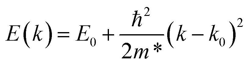
The spin–orbit interaction varies with the square of the atomic mass, yielding an expected splitting size ordering of Pb ≫ Sb > As; however, this is also influenced by the local electric field around the metal centre. From our calculations, we predict that only bournonite will exhibit Rashba splitting, despite the considerably weaker spontaneous polarisation we predict for this material. Bournonite is the only one of the three material that contains Pb, which suggests that the atomic mass of the heavy element is the more dominant factor than the strength of spontaneous polarisation for the Rashba effect. The splitting needs to be sufficient so that for a given temperature and light intensity that the Rashba pockets are partially filled; above this threshold direct band gap behaviour is recovered. For bournonite, we measure an energy difference in the CBM between direct and indirect recombination of approximately 80 meV, whereas kBT at typical solar cell operating temperature of 50 °C is 28 meV, indicating that this indirect behaviour should play a role in an operating solar cell.
5 Conclusions and outlook
We have used a first-principles quantum mechanical approach to assess the optoelectronic properties of the three candidate photoferroic materials: enargite (Cu3AsS4), stephanite (Ag5SbS4) and bournonite (CuPbSbS3). We predicted a direct band gap of 1.24 eV, a direct band gap of 1.59 eV and a slightly indirect band gap of 1.37 eV for enargite, stephanite and bournonite respectively, within the optimal range for a single junction solar cell. We also observe similar features (spin–orbit splitting) in the band structure of bournonite to those associated with the high-performance of hybrid perovskites.93 We predict low electron effective masses for all three materials and heavier holes (see Table 1). We also predict optical dielectric constants, ε∞, again comparable to hybrid perovskites.83We have calculated the spontaneous polarisation density for all three materials and from this we predict that enargite and stephanite will have considerable spontaneous polarisations, comparable to that of standard ferroelectric materials BaTiO3 and PbTiO3. This could suggest that it may be possible to combine a near-optimal band gap (for AM1.5 solar radiation) with ferroelectric–photovoltaic phenomena such as the bulk photovoltaic effect or anomalous photovoltaic effect within these materials. With the upper limit for the power conversion efficiency from these novel PV phenomena still being an open question, these materials could allow for new routes to high efficiency devices.
Our study has shown that the three minerals merit deeper investigation. In addition to further experimental work on synthesis, characterisation and optimisation, the extension of theoretical investigations to include analysis of the defect tolerance of the bulk (beyond the speculation made in this study based on the bonding character of the VBM), and identifying compatible interfaces for high-efficiency devices could help to accelerate the development of these new technologies.
Data access statement
The optimised crystal structures of the three minerals studied are available at https://github.com/wmd-group/crystal_structures. The input and output files for the DFT calculations are available from the online repository NOMAD at http://dx.doi.org/10.17172/nomad/2017.05.16-1.Acknowledgements
This work has been supported by the EPSRC grant no. EP/L016354/1 and EP/K016288/1 (SKW) and by the ERC programme grant no. 277757 (KLS). Part of this work was also supported by the National Science Foundation under Grant No. 1511737 (WPH, TZ, DBM, VB). AW is supported by a Royal Society University Research Fellowship. This work benefited from access to ARCHER, the UK's national high-performance computing service, which is funded by the Office of Science and Technology through EPSRC's High End Computing Programme (Grant no. EP/L000202). We also acknowledge use of Hartree Centre resources in this work through the Energy Materials: Computational Solutions EPSRC project (EP/K016288/1). In particular the author's would like to acknowledge the computational support of Alin Marin Elena. We thank Jarvist M. Frost and Keith T. Butler for fruitful discussions, and Mark Weller, Oliver Weber and Chris Bowen for support and discussions during early stages of the project.References
- N. M. Haegel, R. Margolis, T. Buonassisi, D. Feldman, A. Froitzheim, R. Garabedian, M. Green, S. Glunz, H.-M. Henning, B. Holder, I. Kaizuka, B. Kroposki, K. Matsubara, S. Niki, K. Sakurai, R. A. Schindler, W. Tumas, E. R. Weber, G. Wilson, M. Woodhouse and S. Kurtz, Science, 2017, 356, 141–143 CrossRef CAS PubMed.
- A. Polman, M. Knight, E. C. Garnett, B. Ehrler and W. C. Sinke, Science, 2016, 352, aad4424 CrossRef PubMed.
- W. Shockley and H. J. Queisser, J. Appl. Phys., 1961, 32, 510 CrossRef CAS.
- L. Yu and A. Zunger, Phys. Rev. Lett., 2012, 108, 068701 CrossRef PubMed.
- S. S. Shin, E. J. Yeom, W. S. Yang, S. Hur, M. G. Kim, J. Im, J. Seo, J. H. Noh and S. I. Seok, Science, 2017, 356, 167–171 CrossRef CAS PubMed.
- M. A. Green, A. Ho-Baillie and H. J. Snaith, Nat. Photonics, 2014, 8, 506–514 CrossRef CAS.
- S. K. Wallace, D. B. Mitzi and A. Walsh, ACS Energy Lett., 2017, 2, 776–779 CrossRef CAS.
- I. L. Repins, H. Moutinho, S. G. Choi, A. Kanevce, D. Kuciauskas, P. Dippo, C. L. Beall, J. Carapella, C. DeHart, B. Huang and S. H. Wei, J. Appl. Phys., 2013, 114, 084507 CrossRef.
- N. M. Mangan, R. E. Brandt, V. Steinmann, R. Jaramillo, J. V. Li, J. R. Poindexter, K. Hartman, L. Sun, R. G. Gordon and T. Buonassisi, 2014 IEEE 40th Photovoltaic Specialist Conference (PVSC), 2014 Search PubMed.
- S. D. Stranks, G. E. Eperon, G. Grancini, C. Menelaou, M. J. P. Alcocer, T. Leijtens, L. M. Herz, A. Petrozza and H. J. Snaith, Science, 2013, 342, 341–344 CrossRef CAS PubMed.
- Q. Dong, Y. Fang, Y. Shao, P. Mulligan, J. Qiu, L. Cao and J. Huang, Science, 2015, 347, 967–970 CrossRef CAS PubMed.
- R. E. Brandt, V. Stevanović, D. S. Ginley and T. Buonassisi, MRS Commun., 2015, 5, 265–275 CrossRef CAS.
- J. M. Frost, K. T. Butler, F. Brivio, C. H. Hendon, M. van Schilfgaarde and A. Walsh, Nano Lett., 2014, 14, 2584–2590 CrossRef CAS PubMed.
- H. Guo, P. Liu, S. Zheng, S. Zeng, N. Liu and S. Hong, Curr. Appl. Phys., 2016, 16, 1603–1606 CrossRef.
- P. Wang, J. Zhao, L. Wei, Q. Zhu, S. Xie, J. Liu, X. Meng and J. Li, Nanoscale, 2017, 9, 3806–3817 RSC.
- Y. Rakita, O. Bar-Elli, E. Meirzadeh, H. Kaslasi, Y. Peleg, G. Hodes, I. Lubomirsky, D. Oron, D. Ehre and D. Cahen, Proc. Natl. Acad. Sci. U. S. A., 2017, 201702429 CrossRef PubMed.
- E. I. Parkhomenko, Piezoelectric and Pyroelectric Effects in Minerals, Springer, US, 1971 Search PubMed.
- R. L. Bonewitz, Rocks and Minerals, Dorling Kindersley, Ltd, 2012 Search PubMed.
- V. M. Fridkin, Ferroelectric Semiconductors, Consultants Bureau, 1980 Search PubMed.
- S. Adachi, Earth-Abundant Materials for Solar Cells: Cu2-II-IV-VI4 Semiconductors, Wiley, 2015 Search PubMed.
- A. M. Ganose, C. N. Savory and D. O. Scanlon, Chem. Commun., 2017, 53, 20–44 RSC.
- R. E. Newnham, Properties of Materials, Oxford University Press, 2005 Search PubMed.
- T. L. Bahers, M. Rérat and P. Sautet, J. Phys. Chem. C, 2014, 118, 5997–6008 CAS.
- K. T. Butler, J. M. Frost and A. Walsh, Energy Environ. Sci., 2015, 8, 838–848 CAS.
- V. M. Fridkin, Photoferroelectrics, Springer-Verlag, Berlin, Heidelberg, 1979 Search PubMed.
- B. I. Sturman and V. M. Fridkin, Photovoltaic and Photo-refractive Effects in Noncentrosymmetric Materials, Gordon and Breach Science Publishers, 1992 Search PubMed.
- A. G. Chynoweth, Phys. Rev., 1956, 102, 705–714 CrossRef CAS.
- M. R. Morris, S. R. Pendlebury, J. Hong, S. Dunn and J. R. Durrant, Adv. Mater., 2016, 28, 7123–7128 CrossRef CAS PubMed.
- J. Starkiewicz, L. Sosnowski and O. Simpson, Nature, 1946, 158, 28 CrossRef CAS.
- H. R. Johnson, R. H. Williams and C. H. B. Mee, J. Phys. D: Appl. Phys., 1975, 8, 1530–1541 CrossRef CAS.
- B. Goldstein and L. Pensak, J. Appl. Phys., 1959, 30, 155–161 CrossRef CAS.
- M. D. Uspenskii, N. G. Ivanova and I. E. Malkis, Sov. Phys. Semicond., 1968, 1059 Search PubMed.
- Y. Yuan, Z. Xiao, B. Yang and J. Huang, J. Mater. Chem. A, 2014, 2, 6027–6041 CAS.
- C. Paillard, X. Bai, I. C. Infante, M. Guennou, G. Geneste, M. Alexe, J. Kreisel and B. Dkhil, Adv. Mater., 2016, 28, 5153–5168 CrossRef CAS PubMed.
- W. S. Choi, M. F. Chisholm, D. J. Singh, T. Choi, G. E. Jellison and H. N. Lee, Nat. Commun., 2012, 3, 689 CrossRef PubMed.
- K. T. Butler, S. McKechnie, P. Azarhoosh, M. van Schilfgaarde, D. O. Scanlon and A. Walsh, Appl. Phys. Lett., 2016, 108, 112103 CrossRef.
- E. Fatuzzo, G. Harbeke, W. J. Merz, R. Nitsche, H. Roetschi and W. Ruppel, Phys. Rev., 1962, 127, 2036–2037 CrossRef CAS.
- M. A. García and J. Balenzategui, Renewable Energy, 2004, 29, 1997–2010 CrossRef.
- H. Dittrich, A. Bieniok, U. Brendel, M. Grodzicki and D. Topa, Thin Solid Films, 2007, 515, 5745–5750 CrossRef CAS.
- B. Durant and B. A. Parkinson, 2016 IEEE 43rd Photovoltaic Specialists Conference (PVSC), 2016 Search PubMed.
- H. Dittrich, A. Stadler, D. Topa, H.-J. Schimper and A. Basch, Phys. Status Solidi A, 2009, 206, 1034–1041 CrossRef CAS.
- T. Pauporté and D. Lincot, Adv. Mater. Opt. Electron., 1995, 5, 289–298 CrossRef.
- N. I. Butsko, I. D. Zhezhnich and M. M. Pidorya, Russ. Phys. J., 1973, 16, 223–224 Search PubMed.
- Y. Dong, A. R. Khabibullin, K. Wei, J. R. Salvador, G. S. Nolas and L. M. Woods, ChemPhysChem, 2015, 16, 3264–3270 CrossRef CAS PubMed.
- J. J. Scragg, J. T. Wätjen, M. Edoff, T. Ericson, T. Kubart and C. Platzer-Björkman, J. Am. Chem. Soc., 2012, 134, 19330–19333 CrossRef CAS PubMed.
- V. Blum, R. Gehrke, F. Hanke, P. Havu, V. Havu, X. Ren, K. Reuter and M. Scheffler, Comput. Phys. Commun., 2009, 180, 2175–2196 CrossRef CAS.
- X. Ren, P. Rinke, V. Blum, J. Wieferink, A. Tkatchenko, A. Sanfilippo, K. Reuter and M. Scheffler, New J. Phys., 2012, 14, 053020 CrossRef.
- V. Havu, V. Blum, P. Havu and M. Scheffler, J. Comput. Phys., 2009, 228, 8367–8379 CrossRef CAS.
- S. V. Levchenko, X. Ren, J. Wieferink, R. Johanni, P. Rinke, V. Blum and M. Scheffler, Comput. Phys. Commun., 2015, 192, 60–69 CrossRef CAS.
- A. C. Ihrig, J. Wieferink, I. Y. Zhang, M. Ropo, X. Ren, P. Rinke, M. Scheffler and V. Blum, New J. Phys., 2015, 17, 093020 CrossRef.
- J. Heyd, G. E. Scuseria and M. Ernzerhof, J. Chem. Phys., 2003, 118, 8207–8215 CrossRef CAS.
- W. P. Huhn and V. Blum, arXiv preprint: 1705.01804, 2017.
- E. N. Brothers, A. F. Izmaylov, J. O. Normand, V. Barone and G. E. Scuseria, J. Chem. Phys., 2008, 129, 011102 CrossRef PubMed.
- A. J. Garza and G. E. Scuseria, J. Phys. Chem. Lett., 2016, 7, 4165–4170 CrossRef CAS PubMed.
- G. Bergerhoff and I. Brown, Crystallographic Databases, 1987 Search PubMed.
- K. Momma and F. Izumi, J. Appl. Crystallogr., 2011, 44, 1272–1276 CrossRef CAS.
- C. Ambrosch-Draxl and J. O. Sofo, Comput. Phys. Commun., 2006, 175, 1–14 CrossRef CAS.
- N. A. Spaldin, J. Solid State Chem., 2012, 195, 2–10 CrossRef CAS.
- K. L. Svane and A. Walsh, J. Phys. Chem. C, 2016, 121, 421–429 Search PubMed.
- G. Kresse and J. Furthmüller, Comput. Mater. Sci., 1996, 6, 15–50 CrossRef CAS.
- G. Kresse and J. Furthmüller, Phys. Rev. B: Condens. Matter Mater. Phys., 1996, 54, 11169–11186 CrossRef CAS.
- P. E. Blöchl, Phys. Rev. B: Condens. Matter Mater. Phys., 1994, 50, 17953–17979 CrossRef.
- R. Shuey, Semiconducting Ore Minerals, Elsevier, 2012 Search PubMed.
- L. L. Baranowski, P. Zawadzki, S. Lany, E. S. Toberer and A. Zakutayev, Semicond. Sci. Technol., 2016, 31, 123004 CrossRef.
- F. J. Espinosa-Faller, D. R. Conradson, S. C. Riha, M. B. Martucci, S. J. Fredrick, S. Vogel, A. L. Prieto and S. D. Conradson, J. Phys. Chem. C, 2014, 118, 26292–26303 CAS.
- S. Schorr, H.-J. Hoebler and M. Tovar, Eur. J. Mineral., 2007, 19, 65–73 CrossRef CAS.
- J. J. S. Scragg, L. Choubrac, A. Lafond, T. Ericson and C. Platzer-Björkman, Appl. Phys. Lett., 2014, 104, 041911 CrossRef.
- D. Shin, B. Saparov, T. Zhu, W. P. Huhn, V. Blum and D. B. Mitzi, Chem. Mater., 2016, 28, 4771–4780 CrossRef CAS.
- Z. Xiao, W. Meng, J. V. Li and Y. Yan, ACS Energy Lett., 2017, 2, 29–35 CrossRef CAS.
- T. Gershon, K. Sardashti, O. Gunawan, R. Mankad, S. Singh, Y. S. Lee, J. A. Ott, A. Kummel and R. Haight, Adv. Energy Mater., 2016, 6, 1601182 CrossRef.
- D. Shin, B. Saparov and D. B. Mitzi, Adv. Energy Mater., 2017, 1602366 CrossRef.
- P. Velásquez, D. Leinen, J. Pascual, J. Ramos-Barrado, R. Cordova, H. Gómez and R. Schrebler, J. Electroanal. Chem., 2000, 494, 87–95 CrossRef.
- L. Yu, R. S. Kokenyesi, D. A. Keszler and A. Zunger, Adv. Energy Mater., 2013, 3, 43–48 CrossRef CAS.
- S. Curtarolo, W. Setyawan, G. L. Hart, M. Jahnatek, R. V. Chepulskii, R. H. Taylor, S. Wang, J. Xue, K. Yang, O. Levy, M. J. Mehl, H. T. Stokes, D. O. Demchenko and D. Morgan, Comput. Mater. Sci., 2012, 58, 218–226 CrossRef CAS.
- B. Silvi and A. Savin, Nature, 1994, 371, 683–686 CrossRef CAS.
- A. Walsh, A. A. Sokol, J. Buckeridge, D. O. Scanlon and C. R. A. Catlow, J. Phys. Chem. Lett., 2017, 8, 2074–2075 CrossRef CAS PubMed.
- A. Zakutayev, C. M. Caskey, A. N. Fioretti, D. S. Ginley, J. Vidal, V. Stevanovic, E. Tea and S. Lany, J. Phys. Chem. Lett., 2014, 5, 1117–1125 CrossRef CAS PubMed.
- S. B. Zhang, S.-H. Wei, A. Zunger and H. Katayama-Yoshida, Phys. Rev. B: Condens. Matter Mater. Phys., 1998, 57, 9642–9656 CrossRef CAS.
- C. Persson and A. Zunger, Phys. Rev. Lett., 2003, 91, 266401 CrossRef PubMed.
- C. Persson and A. Zunger, Appl. Phys. Lett., 2005, 87, 211904 CrossRef.
- R. B. Balow, C. K. Miskin, M. M. Abu-Omar and R. Agrawal, Chem. Mater., 2017, 29, 573–578 CrossRef CAS.
- S. D. Wolf, J. Holovsky, S.-J. Moon, P. Löper, B. Niesen, M. Ledinsky, F.-J. Haug, J.-H. Yum and C. Ballif, J. Phys. Chem. Lett., 2014, 5, 1035–1039 CrossRef PubMed.
- F. Brivio, A. B. Walker and A. Walsh, APL Mater., 2013, 1, 042111 CrossRef.
- C. Eames, J. M. Frost, P. R. F. Barnes, B. C. O'Regan, A. Walsh and M. S. Islam, Nat. Commun., 2015, 6, 7497 CrossRef CAS PubMed.
- A. Y. Orlova, R. R. Gainov, A. V. Dooglav, I. N. Pen'kov and E. A. Korolev, JETP Lett., 2012, 96, 370–374 CrossRef CAS.
- K. Wei, J. Martin, J. R. Salvador and G. S. Nolas, Cryst. Growth Des., 2015, 15, 3762–3766 CAS.
- R. Pandeya, G. Vatsc, J. Yund, C. R. Bowen, A. W. Y. Ho-Baillied and J. Seidel, arXiv preprint: 1705.05529, 2017.
- P. S. Brody, Appl. Phys. Lett., 1981, 38, 153–155 CrossRef CAS.
- H.-Y. Huang, M. Wu and L.-J. Qiao, Comput. Mater. Sci., 2014, 82, 1–4 CrossRef CAS.
- R. Wahl, D. Vogtenhuber and G. Kresse, Phys. Rev. B: Condens. Matter Mater. Phys., 2008, 78, 104116 CrossRef.
- Y. Xu, Ferroelectric Materials and Their Applications, North-Holland, 1991 Search PubMed.
- I. Grinberg and A. M. Rappe, Phys. Rev. B: Condens. Matter Mater. Phys., 2004, 70, 220101 CrossRef.
- P. Azarhoosh, S. McKechnie, J. M. Frost, A. Walsh and M. van Schilfgaarde, APL Mater., 2016, 4, 091501 CrossRef.
- F. Zheng, L. Z. Tan, S. Liu and A. M. Rappe, Nano Lett., 2015, 15, 7794–7800 CrossRef CAS PubMed.
- L. D. Whalley, J. M. Frost, Y.-K. Jung and A. Walsh, J. Chem. Phys., 2017, 146, 220901 CrossRef.
Footnote |
| † Electronic supplementary information (ESI) available. See DOI: 10.1039/c7se00277g |
| This journal is © The Royal Society of Chemistry 2017 |