Fabrication of CuInS2 photocathodes on carbon microfiber felt by arc plasma deposition for efficient water splitting under visible light†
Hiroya
Homura
,
Osamu
Tomita
 ,
Masanobu
Higashi
and
Ryu
Abe
*
Graduate School of Engineering, Kyoto University, Katsura, Nishikyo-ku, Kyoto 615-8510, Japan. E-mail: ryu-abe@scl.kyoto-u.ac.jp; Fax: +81 75383 2479; Tel: +81 75383 2479
First published on 20th March 2017
Abstract
An efficient copper indium disulfide (CuInS2) photocathode was fabricated on conductive carbon microfiber felt (CMF), which comprises a three-dimensional (3D) network of carbon fibers (CFs), by the sequential deposition of metal precursors (Cu and In) and subsequent annealing under a stream of diluted H2S. Although the conventional electrochemical deposition method failed to deposit the metal precursors homogeneously on the CMF, the arc plasma deposition (APD) method did so successfully. The unique features of the APD method enabled superior homogeneity of the Cu/In ratio throughout the CMF, not only on the outer surface, but also inside the 3D network, under optimized conditions. Another unique feature of the APD method is its ability to deposit metal species on the back surface of the CFs, thus allowing an almost full-coverage coating of the 3D structure of the CMF substrate. The as-prepared CuInS2/CMF photocathode was further modified with a thin layer of CdS and Pt particles, and then used for photoelectrochemical (PEC) water reduction under visible light. The modified Pt–CdS/CuInS2/CMF photocathode exhibited relatively high incident photon-to-electron conversion efficiency (IPCE) values (ca. 40% at 0 V vs. the RHE under 600 nm) and higher cathodic photocurrent density under continuous visible-light irradiation (λ > 400 nm) than a conventional Pt–CdS/CuInS2 cathode fabricated on a two-dimensional molybdenum substrate. PEC water reduction proceeded stably over the Pt–CdS/CuInS2/CMF photocathode under visible light with almost 100% faradaic efficiency, indicating that CMF is a promising photocathode substrate for PEC water splitting.
Introduction
Photoelectrochemical (PEC) water splitting using semiconductors as photoelectrode materials is a promising system for the clean production of hydrogen (H2) from water utilizing abundant solar light.1 Extensive research effort has been dedicated to developing both photoanodes (n-type semiconductors) and photocathodes (p-type semiconductors) based on various visible-light-responsive semiconductors to achieve efficient PEC water splitting. However, improving their efficiency and developing new materials are still required to demonstrate the feasibility of this H2-production method.1–7 It is well recognized that the performance of photoelectrodes is significantly affected by their structures, both at the macroscopic and microscopic levels. Two types of photoelectrode microstructures have been studied for achieving high-efficiency PEC water splitting: densely packed semiconductor layers (i.e., dense films) on a conducting substrate and porous structures consisting of a network of semiconductor particles on a conducting substrate. The former has often been employed for photocathodes bearing p-type semiconductors, e.g., chalcogenides. However, this type of photoelectrode with a dense semiconductor film has an essential problem in improving the efficiency for PEC water splitting by increasing the thickness of the semiconductor that works as the photoabsorber, when the diffusion distance of carriers in the employed semiconductor is short. In this kind of dense film, the number of photons absorbed by the whole photoelectrode can be increased by increasing the thickness of the semiconductor layers. However, the photocurrent obtained is generally saturated when the thickness reaches a certain level. This saturation is attributed to the limited diffusion distance of minority carriers in the semiconductors. In the case of photocathodes consisting of a p-type semiconductor, most of the photoexcited electrons (i.e., the minority carriers) generated in regions farther from the surface than the average diffusion distance of the electrons cannot reach the solid–liquid interface, because most recombine with holes (both primordial and photogenerated) during migration. Consequently, for this kind of electrode, it is fundamentally difficult to simultaneously achieve sufficient absorption of photons and improved migration of minority carriers, unless the semiconductor material exhibits a remarkably long carrier-diffusion distance.8,9A limited minority-carrier diffusion distance can be mitigated to some degree by using photoelectrodes with porous structures,10–23 as demonstrated in early studies on porous WO3 photoanodes.10,11 In most cases, such porous photoelectrodes comprise layers of spherical semiconductor (nano)particles on a conductive substrate such as fluorine-doped tin oxide (FTO) glass. The semiconductor particles are connected to allow the transfer of majority carriers between the particles and eventually to the conducting substrate. The porous structure enables the minority carriers to react efficiently with substances (e.g., water molecules) that penetrate the pores, because the required migration distance for the minority carriers to the solid–liquid interface is much shorter than those in dense film photoelectrodes. Consequently, the required criteria of sufficient thickness for photoabsorption and efficient utilization of photogenerated minority carriers are simultaneously satisfied.
However, such porous photoelectrodes present another significant issue to be addressed. In many cases, the resistivity at grain boundaries between semiconductor particles inhibits the efficient migration of majority carriers within porous photoelectrodes, necessitating an increased externally applied bias and limiting the improvement of PEC performance.21–23 Photoanodes containing WO3 or Fe2O3 that exhibit a perpendicularly oriented structure24,25 and a dendritic structure,26,27 respectively, have been recently developed to address the issue of efficient majority-carrier migration, and were shown to exhibit superior performance to conventional porous photoanodes, which was attributed to both the high surface area and the highly efficient electron transfer. Such structures have also been introduced into photocathodes based on various p-type semiconductors.28–35
We have recently developed a new type of WO3 photoanode fabricated on three-dimensional (3D) conductive carbon microfiber felt (CMF), which has a macroporous structure.36 Monolayers of fine WO3 particles with diameters of ca. 150 nm were successfully loaded onto the surface of the CMF by simple impregnation with a precursor solution followed by calcination in air, affording higher photocurrent densities and IPCE values for water oxidation under visible light than those of conventional porous WO3/FTO photoanodes.36 Because monolayers of WO3 particles are loaded onto a conductive CMF substrate, the photoexcited electrons can be directly injected into the CMF without passing through grain boundaries, affording high IPCE under monochromatic light. Furthermore, the macroporous structure of CMF can afford a sufficient thickness of the photoabsorber (i.e., WO3 layers) totally, thus resulting in higher photocurrent density under continuous visible light (λ > 400 nm) compared to that on conventional porous WO3/FTO. Thus, this new concept of using CMF as a conductive substrate might enable us to develop efficient photoelectrodes that exhibit both highly efficient migration of carriers and sufficient absorption of photons, not only with WO3, but also with other semiconductors including non-oxide ones.
In the present study, we attempted to apply this concept to the fabrication of an efficient CuInS2 photocathode. Copper-based chalcopyrite semiconductors, such as CuInS2,37–43 Cu(In, Ga)S2,44 CuGaSe2,45 and Cu(In, Ga)Se2,46–49 have been studied as visible-light responsive photocathodes for water splitting because these materials have attractive properties such as high optical absorption coefficients and relatively high carrier mobility. CuInS2 has been extensively studied because it exhibits an appropriate band gap (1.5 eV)43 and a sufficient conduction band bottom for water reduction.44 For example, Ikeda et al. prepared efficient photocathodes comprising CuInS2 on Mo-coated glass substrates using both electrodeposition (ED)37,41,42 and spray pyrolysis methods.44 Both resulting photocathodes were subjected to post-annealing in a H2S stream to form a dense CuInS2 film, and both demonstrated efficient PEC water splitting.
Herein, we attempted to fabricate thin CuInS2 layers on CMF by the sequential deposition of Cu and In using two different methods: an ED method and a cathodic arc-plasma deposition (APD) method.50–53 The obtained precursor samples were finally annealed under a H2S stream to form CuInS2 on the CMF. We have demonstrated for the first time that the use of APD is a promising method to deposit metal precursors homogeneously on the surface of 3D CMF, even on the rear surface, consequently producing highly efficient CuInS2/CMF photocathodes that can stably and efficiently reduce water to H2 under visible light.
Experimental
Deposition of Cu and In onto CMF by arc-plasma deposition (APD)
Sheets of CMF (120 μm thick, 5.8 mΩ cm−2) consisting of carbon fibers (CFs) with diameters of ca. 5–12 μm were provided by Mitsubishi Rayon Co. Ltd. The CMF samples were calcined at 500 °C for 30 min in air prior to use in order to make their surfaces more hydrophilic. No significant change in the morphology was observed after the above-mentioned treatment according to their scanning electron microscopy (SEM) images (see Fig. S1†). To ensure sufficient collection of electrons from the entire CMF material, the top 1.0 × 1.5 cm2 section of the whole 3.0 × 1.5 cm2 CMF sample was impregnated with a conductive carbon paste (Carbon Paint, Structure Probe Inc.), dried, and finally calcined at 500 °C in air for 30 min.The deposition of metal precursors (Cu and In) onto the three-dimensional (3D) CMF (denoted as simply CMF hereafter) was performed by means of arc-plasma deposition (APD, APDT-1S, ADVANCE RIKO Inc.). Cu and In species were deposited on CMF by arc discharge of metallic Cu (99.99%, Nilaco Co., Ltd.) and metallic In (99.9%, Kojundo Chemical Laboratory Co., Ltd.) cathodes, respectively. All the depositions were carried out under vacuum (ca. 5.0 × 10⁻³ Pa) at room temperature. The metal particles were deposited under a range of parameters to establish optimum conditions. For Cu, the number of arc discharge pulses (N) was 3000–20![[thin space (1/6-em)]](https://www.rsc.org/images/entities/char_2009.gif) 000 shots, the capacitance of the condenser (C) was 720–1800 μF, and the voltage for arc discharge (V) was 70–130 V. As will be shown later, the capacitance and voltage were optimized to be 1800 μF and 100 V, respectively, to afford relatively homogeneous deposition of Cu within the CMF substrate. For the deposition of In species, N was 3000–15
000 shots, the capacitance of the condenser (C) was 720–1800 μF, and the voltage for arc discharge (V) was 70–130 V. As will be shown later, the capacitance and voltage were optimized to be 1800 μF and 100 V, respectively, to afford relatively homogeneous deposition of Cu within the CMF substrate. For the deposition of In species, N was 3000–15![[thin space (1/6-em)]](https://www.rsc.org/images/entities/char_2009.gif) 000 shots, C was 360–1800 μF, and V was 70–130 V. The optimum parameters were determined to be 360 μF and 130 V. A reasonable correlation between N and the amount of Cu deposited on the CMF was confirmed, as seen in Fig. S2,† when other conditions were appropriately set (i.e., C: 1800 μF and V: 100 V). A similar correlation was observed for In deposition under optimum conditions (i.e., C: 360 μF and V: 130 V). For the sequential deposition of Cu and In onto the CMF, Cu was first deposited at N: 10
000 shots, C was 360–1800 μF, and V was 70–130 V. The optimum parameters were determined to be 360 μF and 130 V. A reasonable correlation between N and the amount of Cu deposited on the CMF was confirmed, as seen in Fig. S2,† when other conditions were appropriately set (i.e., C: 1800 μF and V: 100 V). A similar correlation was observed for In deposition under optimum conditions (i.e., C: 360 μF and V: 130 V). For the sequential deposition of Cu and In onto the CMF, Cu was first deposited at N: 10![[thin space (1/6-em)]](https://www.rsc.org/images/entities/char_2009.gif) 000 shots, C: 1800 μF, and V: 100 V, and then In was deposited at C: 360 μF and V: 130 V with varying N (5000–12
000 shots, C: 1800 μF, and V: 100 V, and then In was deposited at C: 360 μF and V: 130 V with varying N (5000–12![[thin space (1/6-em)]](https://www.rsc.org/images/entities/char_2009.gif) 000 shots) in order to vary the molar ratio of In to Cu (Cu/In: 0.9–2.2). The samples prepared are denoted as Cu/CMF(APD), In/CMF(APD), and In/Cu/CMF(APD), hereafter.
000 shots) in order to vary the molar ratio of In to Cu (Cu/In: 0.9–2.2). The samples prepared are denoted as Cu/CMF(APD), In/CMF(APD), and In/Cu/CMF(APD), hereafter.
Deposition of Cu and In on CMF by electrochemical deposition (ED)
Electrodeposition (ED) was also employed to deposit Cu and/or In on the CMF, according to previous reports on the preparation of CuInS2 films on Mo substrates (CuInS2/Mo).37,40 An electrochemical cell consisting of a pre-treated CMF working electrode, a Pt counter electrode, and an Ag/AgCl (3.0 M NaCl, 0.209 V vs. the SHE at 25 °C) reference electrode. The applied potential of the working electrode was controlled by using a potentiostat (VersaSTAT 3, Princeton Applied Research Co., Ltd.). For Cu deposition, an aqueous solution (45 mL) containing both 10 mM of CuSO4·5H2O (99.5%, Wako Pure Chemical Co., Ltd.) and 10 mM of citric acid (98%, Wako Pure Chemical Co., Ltd.) was used after adjusting its pH to ca. 2.3 with diluted H2SO4 (0.5 M, Wako Pure Chemical Co., Ltd.). Cu deposition onto the CMF working electrode was then performed with a constant applied potential of −0.6 VAg/AgCl for different time periods (ca. 10–15 min), by which the amount of charge that passed through outer circuit was controlled to be the intended value. The sample prepared is denoted as Cu/CMF(ED), hereafter. For In deposition, an aqueous solution containing 12 mM of InCl3 (99.99%, Alfa Aesar Co., Inc.) was used after adjusting its pH to 2.2 with diluted HCl (0.5 M, Wako Pure Chemical Co., Ltd.). The applied potential was fixed to −0.8 VAg/AgCl. The samples prepared are denoted as In/CMF(ED) and In/Cu/CMF(ED) hereafter. For sequential deposition, the CMF was first deposited with Cu and then with In, according to the deposition procedures described above. The Cu/In ratio was fixed at 1.3, which was the optimum value in previous reports on the preparation of CuInS2/Mo photoelectrodes by ED.38,46 In the present study, the deposited amounts of Cu and/or In on the CMF (or on metallic Mo film in some cases) were controlled by varying the charge density (e.g., Cu: 0.83–2.49 C cm−2).Sulfurization of In/Cu/CMF samples with H2S
The sequentially deposited In/Cu/CMF samples were sulfurized by heating in a stream of H2S according to the procedure shown in a previous report.40 The sample was placed on the inside of a quartz tube (i.d.: 26 mm), and then the gas inside was thoroughly purged with a stream of Ar gas (99.999%, 100 mL min−1) at room temperature. The temperature of the sample was increased to 110 °C at 10 °C min−1 and then maintained for 60 min to produce alloys of Cu and In (e.g., Cu11In9).40 The temperature was then increased to 520 °C at 25 °C min−1. The Ar gas stream was replaced with diluted H2S (5 vol% in Ar, 80 mL min−1) immediately upon reaching 520 °C to avoid the unfavorable formation of a solid solution of In and Cu at high temperatures.40,54,55 After maintaining this sample temperature for 10 min, the stream of H2S/Ar was changed to 99.999% Ar gas (100 mL min−1). Finally, the sample was cooled naturally (see Fig. S3†). The obtained sample was rinsed in Milli-Q grade water, immersed in 10% aqueous KCN37,56,57 for 5 min (to remove the surface CuxS layers that were generated during sulfurization), thoroughly washed with Milli-Q water, and finally dried at room temperature. The obtained material is denoted as CuInS2/CMF, since X-ray diffraction (XRD) analysis confirmed the predominant production of CuInS2 on the CMF. For comparison, CuInS2 samples were also prepared on Mo (99.95%, Nilaco Co., Ltd.) by a process similar to that used for CuInS2/CMF(ED), but using different charge densities (i.e., Cu: 0.83 C cm−2 and In: 0.95 C cm−2), in order to fabricate CuInS2 samples with thicknesses similar to those of the previous report.53Surface modification of CuInS2 cathodes
The CuInS2/CMF samples were modified with a thin layer and/or nanoparticles of CdS, by which charge separation in CuInS2 is generally enhanced,37,58 by a chemical bath deposition (CBD) method according to a previous report.45 Each CuInS2/CMF sample was immersed in 50 mL of an aqueous solution containing both 1.25 mmol of Cd(CH3COO)2 (98.0%, Kanto Chemical Co., Ltd.) and 0.1 mol of NH4OH (28 wt%, Wako Co., Ltd.) at 70 °C for 1 min in order to adsorb Cd2+ onto the CuInS2. Then, 18.75 mmol of SC(NH2)2 (98.0%, Kanto Chemical Co., Ltd.) was added to the solution, and the CuInS2/CMF sample was immersed for 30 s. After the CdS deposition, the sample was placed on the inside of a quartz tube (i.d.: 26 mm), and the gas inside was thoroughly purged with a stream of Ar gas (99.999%, 100 mL min−1) at room temperature. The Ar gas stream was replaced with diluted H2S (5 vol% in Ar, 80 mL min−1), and the temperature of the sample was increased to 200 °C at 25 °C min−1, where it was maintained for 30 min. The sample was then placed in an electric furnace and heated at 200 °C for 30 min. Pt particles as reduction sites for H+ were loaded onto CuInS2/CMF, CuInS2/Mo, CdS/CuInS2/CMF, and CdS/CuInS2/Mo samples by a PEC deposition method under conditions similar to those previously reported.37 The prepared samples were immersed in 0.1 M Na2SO4 (70 mL) containing 0.1 mM of H2PtCl6·6H2O (pH adjusted to 4.0 with HCl), and then irradiated with a Xe lamp (300 W, Cermax, LX-300F) at a potential of −0.1 VAg/AgCl. The time of irradiation was set to 6 min, at which a saturated photocurrent was observed (see Fig. S4†). The obtained samples are denoted as Pt–CuInS2/CMF, Pt–CuInS2/Mo, Pt–CdS/CuInS2/CMF, and Pt–CdS/CuInS2/Mo.Characterization of the fabricated electrodes
The prepared samples were characterized by means of powder XRD (Mini Flex II, Rigaku Co., Ltd., Cu Kα), UV-Vis diffuse reflection spectrophotometry (V-650, JASCO Co., Ltd., reference sample: BaSO4), and SEM (VE-9800, KEYENCE Co., Ltd.). For the top view in the SEM observations, the outer faces that had been directed towards the counter electrode in the ED method, or towards the metal cathode in the APD method, were observed. For the cross-sectional view, the samples were cut through the middle, and the revealed face was observed.Photoelectrochemical measurements
Photoelectrochemical (PEC) measurements were carried out in a PEC cell with a flat window consisting of the prepared electrodes, a Pt counter electrode, and an Ag/AgCl (3.0 M NaCl, +0.209 V vs. the SHE at 25 °C) reference electrode under an Ar atmosphere. Detailed measurement conditions are provided in the ESI.† The IPCE values at each wavelength were calculated using the following equation:| [IPCE (%) = |Iph| × 1240/Plight/λ × 100] |
| HC-STH (%) = [|Iph| × (ERHE − EH+/H2)/Psun] × 100 |
Results and discussion
Deposition of Cu and In species on CMF via the electrodeposition or the arc-plasma deposition method
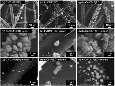
Several highly efficient CuInS2 photocathodes have been prepared by sequential electrodeposition (ED) of Cu and In metals onto conductive substrates such as Mo/glass followed by sulfurization, i.e., heating in diluted H2S.40 Therefore, a similar ED method was applied to the deposition of Cu and In onto three-dimensional (3D) carbon microfiber felt (CMF) substrates. Additionally, an arc-plasma deposition (APD) method was also employed in the present study. In both cases, Cu was first deposited, followed by In deposition, because this sequence produces better CuInS2 photocathodes than deposition in the reverse order.59Fig. 1 shows SEM images of the Cu/CMF and In/CMF samples prepared by ED. These samples are observed from the side that had been facing the counter electrode during ED. In the case of the Cu/CMF(ED) sample, the carbon fibers (CFs) at the outer part of the CMF were entirely and heavily covered by large Cu particles (see Fig. 1(b), an enlarged image of (a)), while only small amounts of Cu particles were found on the CFs inside the CMF (see Fig. 1(c), for example). This inhomogeneous deposition of Cu particles on the CMF is probably due to the inhomogeneous application of electric potentials to the CFs and/or an insufficient supply of Cu inside the thick (ca. 120 μm) CMF. Although various deposition conditions (i.e., different applied potentials, precursors, concentrations, or pH of solutions) as well as different deposition modes (e.g., pulsed electrodeposition) were attempted, homogeneous deposition could not be achieved (not shown). For the In/CMF(ED) samples, only small amounts of In particles are deposited on the CFs both on the surface and inside the CMF, leaving a large portion of the CF surfaces uncovered, as seen in Fig. 1(d)–(i). This might be due to the low activity of the CF surfaces for reduction of the In precursor, resulting in preferential reduction of H+ to H2 during ED. Indeed, the faradaic efficiency for In deposition was estimated to be ca. 60% by comparing the charge passed and the increase in weight. When sequential deposition of In is performed on the Cu/CMF(ED) samples, the size of the particles on the CFs at the outer part significantly increases, as seen in Fig. 1(g) and (h), indicating the efficient deposition of In particles on the Cu. The particles on the CFs inside the CMF also grow to a large size (Fig. 1(i)), implying that the electrochemical reduction of the In precursor is enhanced, even on a small amount of pre-deposited Cu particles.
In contrast, the application of APD with appropriate parameters affords a relatively homogeneous deposition of the metal particles inside the 3D-structured CMF substrate (from the upper to the bottom part), and surprisingly even on the rear surface of the CFs. For example, the cross-sectional views of the Cu/CMF(APD) sample prepared with an optimum combination of parameters (N: 20![[thin space (1/6-em)]](https://www.rsc.org/images/entities/char_2009.gif) 000, C: 1800, and V: 100) are shown in Fig. 2 (whole image (a) and enlarged images in each part (b)–(d)). The deposition of Cu particles is confirmed not only on the CFs in the middle part (c) but also on those in the bottom part (d), while the amount of Cu deposited clearly decreases from the upper to the bottom part. The thicknesses of the Cu layer on each part are estimated to be ca. 300 nm, ca. 50 nm, and ca. 30 nm from the enlarged images ((b), (c′), and (d′)). Interestingly, Cu particles are observed even on the rear side of the CFs (see Fig. 2.). These are unique properties of the APD method, and are in stark contrast to those of other deposition methods, such as sputtering. For example, the conventional sputtering of Au particles on CMF results in deposition of Au only on the front side of the CFs in the upper part of the CMF (see Fig. S5†).
000, C: 1800, and V: 100) are shown in Fig. 2 (whole image (a) and enlarged images in each part (b)–(d)). The deposition of Cu particles is confirmed not only on the CFs in the middle part (c) but also on those in the bottom part (d), while the amount of Cu deposited clearly decreases from the upper to the bottom part. The thicknesses of the Cu layer on each part are estimated to be ca. 300 nm, ca. 50 nm, and ca. 30 nm from the enlarged images ((b), (c′), and (d′)). Interestingly, Cu particles are observed even on the rear side of the CFs (see Fig. 2.). These are unique properties of the APD method, and are in stark contrast to those of other deposition methods, such as sputtering. For example, the conventional sputtering of Au particles on CMF results in deposition of Au only on the front side of the CFs in the upper part of the CMF (see Fig. S5†).
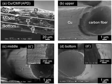 | ||
Fig. 2 Cross-sectional SEM images of the Cu/CMF(APD) sample: capacitance of the condenser (C): 1800 μF, voltage for arc discharge (V): 100 V, and the number of arc discharge pulses: 20![[thin space (1/6-em)]](https://www.rsc.org/images/entities/char_2009.gif) 000 shots. 000 shots. | ||
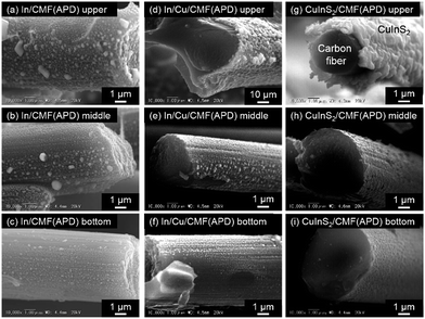
The selection of appropriate conditions (e.g., capacitance (C) and voltage (V)) is indispensable for achieving such a favorable deposition (see Fig. S6†). For example, arc discharge with a low C value (i.e., 720 μF) results in a small amount of Cu particles being deposited in the bottom part (see Fig. S6(a)†), while that with high C values (greater than 1080 μF) affords appreciable deposition, even in the bottom part (see Fig. S6(b) and (c)†). Although the application of higher V deposits more Cu particles in the bottom part (see Fig. S7†), excessively high V (e.g., 130 V) results in inhomogeneous deposition, i.e., the formation of coarse Cu particles (see Fig. S7(c)†). In addition, the CMF substrate collapses when high C (1800 μF) and V (130 V) values are simultaneously applied (data not shown). Thus, the appropriate conditions for Cu deposition were set to be 1800 μF and 100 V. In contrast to the case of Cu deposition, the application of high C (1800 μF) results in exclusive deposition of In particles in the upper part, and In particles are rarely observed in the bottom part (see Fig. S8(c)†). The application of low C (360 μF) affords appreciable deposition even at the bottom part (see Fig. S8(a)†). Thus, the combination of low C (360 μF) and high V (130 V) is appropriate for homogeneous deposition of In particles in the CMF (see Fig. S9(c),† the same images are also shown in Fig. 3(a)–(c)).
The cross-sectional SEM images of In/CMF(APD) and In/Cu/CMF(APD) prepared under the optimized conditions are shown in Fig. 3. Homogeneous deposition of the metal species can be observed from the upper to the bottom part for In/Cu/CMF(APD), which was prepared by sequential deposition of Cu and In under the optimized conditions. As shown above, we found that the APD method has unique features enabling us to deposit the metal particles (Cu and In) even on the CFs inside the CMF that has a 3D structure, while such deposition could not be achieved by conventional ED. Another unique feature of APD is the ability to deposit metal species on the rear surface of the CFs, achieving a full-coverage coating of the CFs in the CMF.
The XRD patterns of the Cu/CMF and In/Cu/CMF samples prepared by ED and APD are shown in Fig. 4(a). The broad peak around 26.4° is attributed to the CMF (graphite, JCPDS 41-1487) substrate. The Cu/CMF(ED) sample is confirmed to contain Cu metal with a tetragonal phase (closed squares), while the In/Cu/CMF(ED) mainly consists of a mixture of the CuIn alloy (squares) and unreacted Cu along with a small fraction of In metal (closed triangles), which is similar to the case of ED on Mo metal substrates, as reported previously.40 The Cu/CMF(APD) also contains metallic Cu with a tetragonal phase, while the In/Cu/CMF(APD) contains the Cu11In9 alloy, which is in contrast to the results for In/Cu/CMF(ED). It has been reported that the Cu11In9 alloy can be formed at above 110 °C, while the CuIn alloy is readily formed at room temperature.40 Thus, it is reasonable to assume that the Cu11In9 in In/Cu/CMF(APD) is formed during APD deposition, in which the energy of the plasma undoubtedly increases the temperature of the samples.
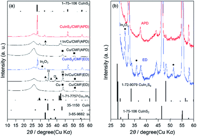 | ||
| Fig. 4 XRD patterns of (a) Cu/CMF, In/Cu/CMF, and CuInS2/CMF samples, and (b) enlarged XRD patterns of CuInS2/CMF samples shown in (a). | ||
Preparation of CuInS2/CMF by sulfurization
The as-prepared In/Cu/CMF samples were sulfurized under a stream of 5% H2S/Ar at 520 °C for 10 min to produce CuInS2 on the CMF, according to the procedure reported by Ikeda et al.37,40 Before sulfurization, the In/Cu/CMF sample was heated in an Ar stream at 110 °C for 1 h to form CuxIn alloys.40 To fabricate a CuInS2 material that shows a p-type nature, a CuxIn alloy with a higher ratio of Cu to In (Cu/In > 1.0) is usually employed as the precursor for sulfurization.37,59,60 Although an excess amount of Cu species generally produces CuxS impurities after such sulfurization, this undesirable CuxS phase can be removed by KCN etching, in which the samples are immersed in 10% aqueous KCN.37,56,57 In the present study, the ratio of Cu to In is fixed to an optimum value of 1.5 unless otherwise stated, as will be shown later.Both the CuInS2/CMF(ED) and CuInS2/CMF(APD) samples, which were obtained by the sulfurization of each In/Cu/CMF sample, exhibit diffraction peaks mainly corresponding to the CuInS2 with a chalcopyrite phase (JCPDS 1-75-106), indicating successful phase transition by sulfurization. However, the CuInS2/CMF(ED) sample exhibits relatively strong peaks derived from In2O3 (JCPDS 1-71-2194), as is clearly seen in Fig. 4. Additionally, the weak peaks derived from CuIn5S8 (JCPDS 1-72-9079) are clearly observed for CuInS2/CMF(ED) (see Fig. 4(b)). This formation of impurities indicates that the present ED method results in inhomogeneous deposition of Cu and In, i.e., significantly different Cu/In ratios from place to place. Conversely, no peaks corresponding to In2O3 are observed for CuInS2/CMF(APD). Although peaks derived from CuIn5S8 are appreciable (see Fig. 4(b)), these peaks are significantly weaker compared to those of CuInS2/CMF(ED). These findings strongly suggest that the use of APD achieves better homogeneity in the Cu/In ratio throughout the entire CMF structure. It should be noted that no diffraction peaks derived from excess Cu species such as CuxS are observed for both CuInS2/CMF samples, despite these samples being prepared with excess Cu (Cu/In = 1.5), as described above. It is known that the CuInS2 phase can be obtained by the sulfurization of precursors in a wide range of Cu/In ratios (from 1–1.8), accompanied by the formation of CuxS phases, which are amorphous in most cases.37,59 It appears that diffraction peaks derived from CuxS are not observed for the present CuInS2/CMF samples because the CuxS produced is amorphous; however, the samples certainly contain CuxS species to some extent. Therefore, no obvious change is observed in the XRD patterns of the CuInS2/CMF samples after KCN etching, which was employed to remove such CuxS impurities (see Fig. S10†).37 However, the color of the samples clearly changes upon KCN etching (not shown), as was also reported by Ikeda et al.37 Also, the XPS analysis indicated the obvious decrease in the Cu/In ratio from 1.4 to 0.9 after the KCN etching, whereas no significant change in the binding energy of each element (Cu and In) was observed. These results indicated the successful removal of CuxS from the surfaces.
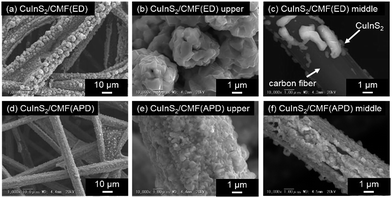
Fig. 5 shows the top-view SEM images of CuInS2/CMF samples prepared using both ED ((a)–(c)) and APD ((d)–(f)), all of which were treated with KCN. In the case of CuInS2/CMF(ED), only the upper part is covered by large CuInS2 particles, while only a limited number of particles are detected in the middle part, as may be reasonably expected from the inhomogeneous deposition of each precursor (Cu and In) demonstrated in Fig. 1. Conversely, both the upper and middle parts of CuInS2/CMF(APD) are almost entirely covered with CuInS2 particles, while exposed CF surfaces can be seen in limited regions in the middle part (see Fig. 5(f)). These exposed surfaces are probably formed upon the removal of CuxS species during the KCN etching process. As shown in Fig. 3(g)–(i), CuInS2 particles are also deposited on the bottom part of CuInS2/CMF(APD), while the amount of particles gradually decreases from the upper to the bottom part. The thickness of the CuInS2 on the upper part is ca. 0.5–1.0 μm (see Fig. 3(g)). It should be noted that even the rear side of the CFs is coated with CuInS2 particles. These results indicate that the APD method affords much better homogeneity in CuInS2 loading throughout the entire CMF structure (i.e., from the upper to the bottom part) compared to that achievable with conventional ED.
Photoelectrochemical properties of Pt-loaded CuInS2/CMF samples
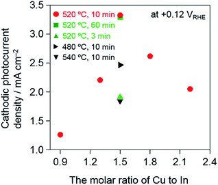
The PEC performance of the CuInS2/CMF samples was evaluated in 0.5 M Na2SO4 under visible-light irradiation after PEC deposition of Pt particles on the surface as a cocatalyst for water reduction. These samples were prepared under the optimum conditions (i.e., Cu/In = 1.5, sulfurization at 520 °C for 10 min, and etching with KCN). As shown in Fig. 6, the Pt–CuInS2/CMF(APD) (see (b)) exhibits a much higher cathodic photocurrent than Pt–CuInS2/CMF(ED) (see (a)). The higher photocurrent over the APD sample is due to the higher homogeneity of the CuInS2 particles deposited throughout the CMF than that of the ED sample, as is clearly seen in the SEM images (see Fig. 5). The photocurrent over the CuInS2/CMF(APD) sample is significantly increased by KCN etching (see Fig. S11† for example), indicating the successful removal of amorphous phase CuxS that generally inhibits electron transfer. This significant enhancement by the removal of excess CuxS implies that the Cu/In ratio employed in the preparation procedure affects the performance of CuInS2/CMF photocathodes, because higher Cu/In ratios induce a larger amount of CuxS. Furthermore, it has been reported that the Cu/In ratio has a significant influence on the various properties of CuInS2, such as resistance, carrier density, and carrier mobility.60–63 Indeed, the Cu/In ratio significantly affects the photocurrent density over the CuInS2/CMF(APD) samples that were prepared by sulfurization at 520 °C for 10 min, as seen in Fig. 7 (the amount of Cu deposited was fixed). The maximum photocurrent is obtained with a Cu/In ratio of 1.5, with higher Cu/In ratios (1.8 and 2.2) resulting in lower photocurrent. The surplus Cu species undoubtedly produce a larger amount of CuxS during sulfurization, most of which will be removed upon KCN etching, resulting in a lower amount of active CuInS2 on the CMF, while the influence of changes in other properties of CuInS2 cannot be completely excluded. It is also confirmed that the temperature and duration of sulfurization affect the photocurrent (see Fig. 7). The optimum conditions were confirmed to be 520 °C for 10 min, as previously reported by Ikeda et al. for CuInS2 photocathodes prepared on a Mo-coated glass substrate.37 Thus, the conditions for sulfurization were fixed at 520 °C for 10 min for all subsequent investigation.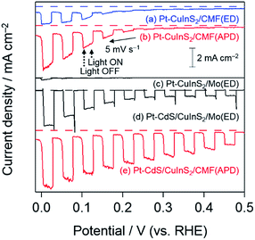 | ||
| Fig. 6 Current–potential curves of Pt–CuInS2 and Pt–CdS/CuInS2 photocathodes in 0.5 M Na2SO4 aq. (pH 4.0, adjusted by using H2SO4) under chopped visible light irradiation (λ > 400 nm). | ||
Photoelectrochemical properties of the Pt–CdS/CuInS2/CMF photocathode
As shown above, the Pt–CuInS2/CMF(APD) photocathode exhibits a higher photocurrent than the Pt–CuInS2/CMF(ED) photocathode (see Fig. 6), indicating the ability of APD to produce CuInS2 particles throughout the entire CMF substrate. Various techniques such as surface modification have been studied for performance enhancement of Pt–CuInS2 photocathodes.37–39,41 For example, Ikeda et al. have reported that the formation of a p–n junction between p-type CuInS2 and n-type CdS, i.e., surface modification with a thin layer of CdS, suppresses electron–hole recombination, resulting in increased cathodic photocurrent.37–39 Thus, the present CuInS2/CMF(APD) samples were also subjected to surface modification with CdS layers by chemical bath deposition (CBD) accompanied by post-annealing.The XRD pattern of the CuInS2/CMF(APD) sample after the CBD of CdS and subsequent post-annealing under a 5% H2S/Ar stream at 200 °C for 30 min indicates the formation of cubic phase CdS (see Fig. S12†). The SEM image of the sample (see Fig. S13†) also indicates successful modification by thin-layer CdS; fine particles are observed after CBD, while no such particles are observed before the treatment. Although post-annealing was carried out in air at 200 °C in a previous report,58 we found that post-annealing under a 5% H2S/Ar stream at the same temperature results in better cathodic photocurrent (see Fig. S14†). Thus, post-annealing under 5% H2S/Ar stream was employed for all subsequent studies. The annealed CdS/CuInS2/CMF samples were subsequently deposited with Pt particles as water reduction sites by the same procedure as that used for the CuInS2/CMF samples. The molar ratio of Pt to Cu and that of Cd to Cu were determined to be about 0.2 and 0.3, respectively, from the XP spectra.
The current–potential curves of the Pt–CdS/CuInS2 photocathodes are shown in Fig. 6. The surface modification of CuInS2/CMF(APD) by CdS followed by Pt results in a significant anodic shift in the onset potential compared with that of Pt–CuInS2/CMF(APD) from ca. 0.3 to ca. 0.65 V vs. the RHE (see Fig. 6(b) and 8(a), respectively), accompanied by a significant increase in the photocurrent density over the whole potential range. Since the valance band maximum is located at around +0.7 V vs. the SHE according to the previous report,44 the ideal onset potential will be ca. +0.7 V if assuming negligibly low over potentials and resistances. The observed onset potential at +0.65 V is relatively close to the ideal value and therefore indicates the fairly good features of the present photocathodes. Such onset potential shift and enhanced photocurrent density have been reported in previous reports on CuInS2 prepared on Mo-coated glass substrates, and were explained by the enhanced charge separation upon formation of a p–n junction.37 We also prepared Pt–CdS/CuInS2 on a Mo-metal substrate by basically the same procedure as that reported by Ikeda et al.37 and compared the performances. The thickness of CuInS2 was fixed at 1.5 μm, as previously reported.37 As seen in Fig. 6, the CdS-modification of CuInS2/Mo(ED) drastically increases the photocurrent and induces a significant shift in the onset potential, as reported. The photocurrent density on Pt–CdS/CuInS2/Mo(ED) is comparable to the reported values under similar conditions, confirming the fairness of the comparison. As is clearly seen in Fig. 6, the Pt–CdS/CuInS2/CMF(APD) photocathode exhibits significantly higher photocurrent, especially at more positive potentials (from 0.1 to 0.5 V vs. RHE), i.e., under lower applied potentials. This higher photocurrent at lower applied potentials strongly indicates that the photogenerated charge is more efficiently separated in the Pt–CdS/CuInS2/CMF(APD) photocathode system than in the conventional Pt–CdS/CuInS2/Mo(ED), which is due to the thinner CuInS2 layer (from 0.2 to 1.0 μm, depending on location) in the former compared to that in the latter (ca. 1.5 μm). In the case of conventional photocathodes (and also photoanodes) fabricated on a two-dimensional substrate such as Mo/glass, a relatively thick semiconductor layer is required to afford effective absorbance of incident photons. However, increasing the semiconductor thickness adversely increases the probability of charge recombination in the semiconductor bulk, due to the short diffusion distance of minority carriers. Conversely, substantial photon absorption can be achieved totally by the relatively thin semiconductor layers deposited on the present CMF substrate. These results demonstrate the advantage of photocathode systems fabricated on CMF substrates for achieving highly efficient photon-to-current conversion, even at lower applied potentials.
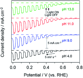
Fig. 8 shows the current–potential curves of the Pt–CdS/CuInS2/CMF(APD) photocathode measured at various pH values under AM 1.5 G simulated solar light (100 mW cm−2). The photocurrent density of the Pt–CdS/CuInS2/CMF(APD) photocathode increases with increasing pH up to 11.0, and then slightly decreases at pH 13.0. The decrease at pH 13.0 is probably due to the excessively decreased H+ concentration. It has been reported that the band edge potentials of Cu(Ga, In)S2 samples shift to positive values with an increase in pH.64 Conversely, those of CdS samples do not depend on the pH, as reported previously.65 Therefore, the formation of steep band bending at the n-CdS/p-CuInS2 junction in alkaline solution is considered to suppress the recombination of photogenerated electrons and holes, resulting in an increase in the photocurrent density.37,58 Therefore, the formation of steep band bending at the n-CdS/p-CuInS2 junction in alkaline solution is considered to suppress the recombination of photogenerated electrons and holes, resulting in a slight shift of the onset to positive potentials and an increase in the photocurrent density.
Conversion efficiency of the Pt–CdS/CuInS2/CMF photocathode in the hydrogen evolution reaction (HER)
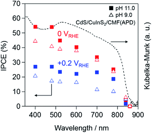
As shown above, the Pt–CdS/CuInS2/CMF(APD) photocathode exhibits the highest performance in 0.1 M Na2HPO4 at pH 11.0 under AM 1.5 G simulated solar light (100 mW cm−2). The results strongly suggest that the higher photocurrent of the Pt–CdS/CuInS2/CMF(APD) sample is due to the improved charge separation in the thinner CuInS2 layers on the CMF. Next, we evaluated its performance by IPCE measurement. Fig. 9 shows the IPCE plots of the Pt–CdS/CuInS2/CMF(APD) photocathode measured at 0 and +0.2 VRHE in pH 9.0 and 11.0 sodium phosphate buffer solutions, along with the photoabsorption spectrum of CdS/CuInS2/CMF (dashed line). The onsets of the IPCE plots largely coincide with the photoabsorption edge, indicating that the cathodic photocurrent is derived from the band gap transition (ca. 1.5 eV). The IPCE values obtained from Pt–CdS/CuInS2/CMF(APD) measured at pH 11.0 are higher than those at pH 9.0. (pH 11.0: 40%, pH 9.0: 38%, at 600 nm under an applied potential of 0 VRHE). The IPCE value of the Pt–CdS/CuInS2/CMF(APD) photocathode obtained at 600 nm under pH 9.0 is higher than the previously reported value for a Pt–CdS/CuInS2/Mo/glass photocathode (i.e., 24% at 600 nm under 0 VRHE)44 when compared at the same pH, while the values at pH 11.0 have not been previously reported. It should be noted that the Pt–CdS/CuInS2/CMF(APD) photocathode exhibits relatively high IPCE values above 20%, even under a lower applied potential of +0.2 VRHE in the range of 400–700 nm at pH 11.0 (see Fig. 9).These results strongly suggest that electron transfer proceeds efficiently between CuInS2 and the CMF, owing to the smaller amount of grain boundaries in the relatively thin layer of CuInS2.
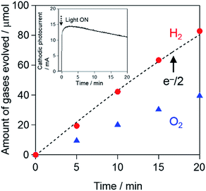
Fig. 10 shows the time course of gas evolution using the Pt–CdS/CuInS2/CMF(APD) photocathode in a two-component PEC cell separated by a porous glass filter at +0.2 VRHE in 0.1 M sodium phosphate buffer solution (pH 11.0) under AM 1.5 G simulated solar light (100 mW cm−2). The amount of H2 gas evolved over the Pt–CdS/CuInS2/CMF(APD) photocathode agrees well with half the amount of electrons passed through the outer circuit (e−/2: dotted line), indicating almost 100% faradaic efficiency. Such a high faradaic efficiency strongly suggests that the CMF material is a durable substrate for the preparation of photocathodes for PEC water splitting. The amount of H2 evolved over the Pt–CdS/CuInS2/CMF(APD) photocathode is close to the stoichiometric amount of O2 (i.e., H2: 82.8 μmol and O2: 39.5 μmol after 20 min). The turnover numbers for H2 evolution are estimated to be ca. 41 (based on ca. 2 μmol of CdS) and ca. 7.5 (based on ca. 11 μmol of CuInS2), indicating that PEC water splitting on Pt–CdS/CuInS2/CMF(APD) proceeds photoelectrochemically. However, the gas evolution rates, as well as the cathodic photocurrent, gradually decrease with the progress of the reaction (Fig. S15†). A similar gradual decrease was also observed for the previously reported Pt–CdS/CuInS2/Mo/glass photocathodes, and was explained by the occurrence of photocorrosion of CdS.39,49 XPS analysis clearly confirmed the decrease in Cd contents after the PEC reaction (see Fig. S15†). As seen in Fig. S16,† most of the fine particles observed on the surface of Pt–CdS/CuInS2(APD) before the reaction vanished after the PEC reaction, further confirming the occurrence of photocorrosion. The decreased photocurrent during the 1st run was slightly recovered to some extent under the subsequent light irradiation after 20 min of interval under dark conditions (see Fig. S17†), suggesting that the accumulation of bubbles is one of the reasons for the decrease of the photocurrent. However, the photocurrent was not recovered completely and then gradually decreased in the 2nd run with prolonged time. These data indicated that the reason for the decreased photocurrent is basically the occurrence of photocorrosion of CdS particles. Recently, the surface modification of CuInS2 photocathodes with other oxide materials such as n-type TiO2 layers has demonstrated to not only increase but also stabilize the cathodic photocurrent, affording highly stable H2 production.28 Such surface modifications are now under investigation; the results will be reported in near future.
Fig. 11 shows the HC-STH of the Pt–CdS/CuInS2/CMF(APD) photocathode calculated using the above current–potential curves (see Fig. 8) with 100% faradaic efficiency based on the results of the HER (see Fig. 10). The highest HC-STH of the Pt–CdS/CuInS2/CMF(APD) photocathode is obtained at pH 11.0, and the highest efficiency of 0.91% is obtained at both +0.27 and +0.31 VRHE.
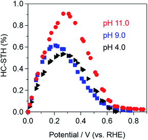 | ||
| Fig. 11 Half-cell solar-to-hydrogen conversion efficiency (HC-STH) of the Pt–CdS/CuInS2/CMF(APD) photocathode in various pH aqueous sodium phosphate buffer solutions under simulated solar light irradiation (AM 1.5 G, 100 mW cm−2). HC-STH was calculated from the current–potential curves of the Pt–CdS/CuInS2/CMF(APD) photocathode shown in Fig. 8. | ||
Conclusions
In summary, a new type of photocathode consisting of densely packed layers of a CuInS2 photoabsorber loaded on conductive CMF having a macroscopic 3D network structure has been fabricated for the first time and demonstrated to exhibit a fairly high efficiency for PEC water reduction to H2 under visible light. It was also demonstrated for the first time that APD of metal precursors (Cu and In) under optimized conditions affords better homogeneity of Cu/In ratios throughout the CMF structure, in addition to their deposition even on the back surface of CFs.The prepared CuInS2/CMF photocathode exhibited relatively high IPCE values (ca. 40% at 0 V vs. the RHE under 600 nm) along with a high cathodic photocurrent density under continuous visible-light irradiation (λ > 400 nm) after surface modification with n-type CdS and a Pt cocatalyst. The obtained cathodic photocurrent density was higher than that of conventional Pt–CdS/CuInS2 fabricated on a two-dimensional Mo-metal substrate. The results strongly suggested that electron transfer proceeds efficiently from the conductive CMF substrate to the CuInS2 semiconductor to the smaller amount of grain boundaries in the relatively thin layer of CuInS2, while sufficient photoabsorption can be achieved by the macroporous 3D structure of CMF. The almost 100% faradaic efficiency for water reduction over the Pt–CdS/CuInS2/CMF photocathode implies the durability of the CMF as a substrate for photocathodes, while the insufficient stability of Pt–CdS/CuInS2/CMF owing to photocorrosion of the CdS layer must be addressed. Although the stability of the CMF against oxidation (electrochemical and/or chemical) might be insufficient, the CMF is stable under reductive atmospheres (e.g., H2, NH3, and H2S), as well as under oxygen-free environments, even at high temperatures. Thus, the combination of a CMF substrate with non-oxide semiconductors (e.g., nitrides, halides, sulfides etc.) will be one of the attractive strategies for fabricating efficient photoelectrodes toward PEC water splitting.
Acknowledgements
This work was financially supported by the ENEOS Hydrogen Trust Fund and by the JSPS Grant-in-Aid for Scientific Research (b) (Grant Number 15H03849) and by SICORP, JST. The authors are indebted to the technical division of the Institute for Catalysis, Hokkaido University for their help in building the experimental equipment.Notes and references
- A. J. Nozik, J. Phys. Chem., 1996, 100, 13061 CrossRef CAS.
- A. J. Nozik, Annu. Rev. Phys. Chem., 1978, 29, 189 CrossRef CAS.
- A. Heller, Acc. Chem. Res., 1981, 14, 154 CrossRef CAS.
- M. Grätzel, Nature, 2001, 414, 338 CrossRef PubMed.
- M. G. Walter, E. L. Warren, J. R. Mckone, S. W. Boettcher, Q. Mi, E. A. Santori and N. S. Lewis, Chem. Rev., 2010, 110, 6446 CrossRef CAS PubMed.
- R. Abe, J. Photochem. Photobiol., C, 2010, 11, 179 CrossRef CAS.
- T. Hisatomi, J. Kubota and K. Domen, Chem. Soc. Rev., 2014, 43, 7520 RSC.
- S. Sodergren, A. Hagfeldt, J. Olsson and S. E. Lindquist, J. Phys. Chem., 1994, 98, 5556 Search PubMed.
- J. Wang, J. Zhao and F. E. Osterloh, Energy Environ. Sci., 2015, 8, 2970 CAS.
- C. Santato, M. Ulmann and J. Augustynski, J. Phys. Chem. B, 2001, 105, 936 CrossRef CAS.
- B. D. Alexander, P. J. Kulssza, I. Rutkowska, R. Solarska and J. Augustynski, J. Mater. Chem., 2008, 18, 2298 RSC.
- Y. H. Ng, A. Iwase, N. J. Bell, A. Kudo and R. Amal, Catal. Today, 2011, 164, 353 CrossRef CAS.
- J. A. Seabold and K.-S. Choi, Chem. Mater., 2011, 23, 1105 CrossRef CAS.
- K. Sivula, R. Zboril, F. L. Formal, R. Robert, A. Weidenkaff, J. Tucek, J. Frydrych and M. Grätzel, J. Am. Chem. Soc., 2010, 132, 7436 CrossRef CAS PubMed.
- M. Barroso, A. J. Cowan, S. R. Pendlebury, M. Grätzel, D. R. Klug and J. R. Durrant, J. Am. Chem. Soc., 2011, 133, 14868 CrossRef CAS PubMed.
- K. J. McDonald and K.-S. Choi, Chem. Mater., 2011, 23, 1686 CrossRef CAS.
- A. Kay, L. Cesar and M. Grätzel, J. Am. Chem. Soc., 2006, 128, 15714 CrossRef CAS PubMed.
- I. Cesar, K. Sivula, A. Kay, R. Zboril and M. Grätzel, J. Phys. Chem. C, 2009, 113, 772 CAS.
- R. Abe, M. Higashi and K. Domen, J. Am. Chem. Soc., 2010, 132, 11828 CrossRef CAS PubMed.
- M. Higashi, K. Domen and R. Abe, J. Am. Chem. Soc., 2011, 134, 6968 CrossRef PubMed.
- U. Björkstén, J. Moser and M. Grätzel, Chem. Mater., 1994, 6, 858 CrossRef.
- N. Beermann, L. Vayssieres, S. E. Lindquist and A. Hagfeldt, J. Electrochem. Soc., 2000, 147, 2456 CrossRef CAS.
- B. Yang, P. R. F. Barnes, W. Bertram and V. Luca, J. Mater. Chem., 2007, 17, 2722 RSC.
- F. Amano, D. Li and B. Ohtani, Chem. Commun., 2010, 46, 2769 RSC.
- F. Amano, M. Tian, G. Wu, B. Ohtani and A. Chen, ACS Appl. Mater. Interfaces, 2011, 3, 4047 CAS.
- A. Kay, L. Cesar and M. Grätzel, J. Am. Chem. Soc., 2006, 128, 15714 CrossRef CAS PubMed.
- I. Cesar, K. Sivula, A. Kay, R. Zboril and M. Grätzel, J. Phys. Chem. C, 2009, 113, 772 CAS.
- J. Zhao, T. Minegishi, L. Zhang, M. Zhong, G. Gunawan, M. Nakabayashi, G. Ma, T. Hisatomi, M. Katayama, S. Ikeda, N. Shibata, T. Yamada and K. Domen, Angew. Chem., Int. Ed., 2014, 53, 11808 CrossRef CAS PubMed.
- Z. Guan, W. Luo, J. Feng, Q. Tao, Y. Xu, X. Wen, G. Fu and Z. Zou, J. Mater. Chem. A, 2015, 3, 7840 CAS.
- X. Wen, W. Luo and Z. Zou, J. Mater. Chem. A, 2013, 1, 15479 CAS.
- C. G. Read, Y. Park and K.-S. Choi, J. Phys. Chem. Lett., 2013, 3, 1872 CrossRef PubMed.
- M. X. Zhuang, A. X. Wei, Y. Zhao, J. Liu, Z. Q. Yan and Z. Liu, Int. J. Hydrogen Energy, 2015, 40, 806 CrossRef CAS.
- R. German, A. Harush and I. Visoly-Fisher, J. Phys. Chem. C, 2015, 119, 1683 Search PubMed.
- J. Wu, Y. Li, J. Kubota, K. Domen, M. Aagesen, T. Ward, A. Snchez, R. Beanland, Y. Zhang, M. Tang, S. Hatch, A. Seeds and H. Liu, Nano Lett., 2014, 14, 2013 CrossRef CAS PubMed.
- L. Gao, Y. Cui, J. Wang, A. Cavalli, A. Standing, T. T. T. Vu, M. A. Verhejen, J. E. M. Haverkort, E. P. A. M. Bakkers and P. H. L. Notten, Nano Lett., 2014, 14, 3715 CrossRef CAS PubMed.
- H. Homura, B. Ohtani and R. Abe, Chem. Lett., 2014, 43, 1195 CrossRef CAS.
- S. Ikeda, T. Nakamura, S. M. Lee, T. Yagi, T. Harada, T. Minegishi and M. Matsumura, ChemSusChem, 2011, 4, 262 CAS.
- G. Gunawan, W. Septina, S. Ikeda, T. Harada, T. Minegishi, K. Domen and M. Matsumura, Chem. Commun., 2014, 50, 8941 RSC.
- J. Zhao, T. Minegishi, L. Zhang, M. Zhong, G. Gunawan, M. Nakabayashi, G. Ma, T. Hisatomi, M. Katayama, S. Ikeda, N. Shibata, T. Yamada and K. Domen, Angew. Chem., Int. Ed., 2014, 53, 11808 CrossRef CAS PubMed.
- S. M. Lee, S. Ikeda, T. Yagi, T. Harada, A. Ennaoui and M. Matsumura, Phys. Chem. Chem. Phys., 2011, 13, 6662 RSC.
- J. Luo, S. D. Tilley, L. Steier, M. Schreier, M. T. Mayer, H. J. Fan and M. Grätzel, Nano Lett., 2015, 15, 1395 CrossRef CAS PubMed.
- K. Iwashina, A. Iwase, Y. H. Ng, R. Amal and A. Kudo, J. Am. Chem. Soc., 2015, 137, 604 CrossRef CAS PubMed.
- M. Krunks, O. Bijakina, V. Varema, V. Miki and E. Mellikov, Thin Solid Films, 1999, 338, 125 CrossRef CAS.
- W. Septina, G. Gunawan, S. Ikeda, T. Harada, M. Higashi, R. Abe and M. Matsumura, J. Phys. Chem. C, 2015, 119, 8576 CAS.
- H. Kumagai, T. Minegishi, Y. Moriya, J. Kubota and K. Domen, J. Phys. Chem. C, 2014, 118, 16386 CAS.
- R. C. Valderrama, P. J. Sebastian, J. P. Enriquez and S. A. Gamboa, Sol. Energy Mater. Sol. Cells, 2005, 88, 145 CrossRef CAS.
- D. Yokoyama, T. Minegishi, K. Maeda, M. Katayama, J. Kubota, A. Yamada, M. Konagai and K. Domen, Electrochem. Commun., 2010, 12, 851 CrossRef CAS.
- T. J. Jacobsson, C. Platzer-Björkman, M. Edoff and T. Edvinsson, Int. J. Hydrogen Energy, 2013, 38, 15027 CrossRef CAS.
- H. Kumagai, T. Minegishi, N. Sato, T. Yamada, J. Kubota and K. Domen, J. Mater. Chem. A, 2015, 3, 8300 CAS.
- Y. Agawa, S. Endo, M. Matsuura and Y. Ishii, Adv. Mater. Res., 2010, 123–125, 1067 CrossRef CAS.
- Y. Agawa, H. Tanaka, S. Torisu, S. Endo, A. Tsujimoto, N. Gonohe, V. Malgras, A. Aldalbahi, S.-M. Alshehri, Y. Kamachi, C. Li and Y. Yamauchi, Sci. Technol. Adv. Mater., 2015, 16, 024804 CrossRef PubMed.
- S. Hinokuma, K. Murakami, K. Uemura, M. Matsuda, K. Ikeue, N. Tsukahara and M. Machida, Top. Catal., 2009, 52, 2108 CrossRef CAS.
- S. Hinokuma, H. Fujii, Y. Katsuhara, K. Ikeue and M. Machida, Catal. Sci. Technol., 2014, 4, 2990 CAS.
- M. Joswing, M. Gossla, H. Metzner, U. Reisöhner, Th. Hahn and W. Witthuhn, Thin Solid Films, 2007, 515, 5921 CrossRef.
- H. Rodriguez-Alvarez, I. M. Koetschau, C. Genzel and H. W. Schock, Thin Solid Films, 2009, 517, 2140 CrossRef CAS.
- J. Klaery, J. Bruns, R. Henninger, K. Siemer, R. Klenk, K. Ellmer and D. Bräuning, Semicond. Sci. Technol., 1998, 13, 1456 CrossRef.
- Y. Onuma, K. Takeuchi, S. Ichikawa, M. Harada, H. Tanaka, A. Koizumi and Y. Miyajima, Sol. Energy Mater. Sol. Cells, 2011, 69, 261 CrossRef.
- D. Yokoyama, T. Minegishi, K. Maeda, M. Katayama, J. Kubota, A. Yamada, M. Konagai and K. Domen, Electrochem. Commun., 2010, 12, 851 CrossRef CAS.
- J. Herrero and J. Ortega, Sol. Energy Mater., 1990, 20, 53 CrossRef CAS.
- S. Yong, J. Zhengguo, L. Chunyan, A. Hesong and Q. Jijun, Appl. Surf. Sci., 2006, 252, 3737 CrossRef.
- G. K. Padam and S. U. M. Rao, Sol. Energy Mater., 1986, 13, 297 CrossRef CAS.
- J. Herrero and J. Ortega, Sol. Energy Mater., 1990, 20, 53 CrossRef CAS.
- S. Nakamura and A. Yamamoto, Sol. Energy Mater. Sol. Cells, 2003, 75, 81 CrossRef CAS.
- A. M. Fernández, N. Dheree, J. A. Turner, A. M. Martinez, L. G. Arriaga and U. Cano, Sol. Energy Mater. Sol. Cells, 2005, 85, 251 CrossRef.
- T. Watanabe, A. Fujishima, O. Tatsuoki and K. Honda, Bull. Chem. Soc. Jpn., 1976, 49(1), 8 CrossRef CAS.
Footnote |
| † Electronic supplementary information (ESI) available: SEM images of the as-provided CMF, XRD patterns of CuInS2/CMF samples before and after the KCN etching, influence of the KCN etching on the current density of CuInS2/CMF(APD) samples, XRD patterns of CdS/CuInS2/CMF(APD) samples prepared by chemical bath deposition etc. See DOI: 10.1039/c7se00008a |
| This journal is © The Royal Society of Chemistry 2017 |

