
 Open Access Article
 This Open Access Article is licensed under a Creative Commons Attribution-Non Commercial 3.0 Unported Licence
Flexible inorganic light emitting diodes based on semiconductor nanowires
Nan
Guan
a,
Xing
Dai
a,
Andrey V.
Babichev
 abc,
François H.
Julien
a and
Maria
Tchernycheva
*a
abc,
François H.
Julien
a and
Maria
Tchernycheva
*a
aCentre de Nanosciences et de Nanotechnologies, UMR9001 CNRS, University Paris Sud, University Paris Saclay, 91405 Orsay, France. E-mail: maria.tchernycheva@u-psud.fr
bITMO University, 197101 St. Petersburg, Russia
cIoffe Institute, 194021 St. Petersburg, Russia
First published on 2nd October 2017
Abstract
The fabrication technologies and the performance of flexible nanowire light emitting diodes (LEDs) are reviewed. We first introduce the existing approaches for flexible LED fabrication, which are dominated by organic technologies, and we briefly discuss the increasing research effort on flexible inorganic LEDs achieved by micro-structuring and transfer of conventional thin films. Then, flexible nanowire-based LEDs are presented and two main fabrication technologies are discussed: direct growth on a flexible substrate and nanowire membrane formation and transfer. The performance of blue, green, white and bi-color flexible LEDs fabricated following the transfer approach is discussed in more detail.
Introduction
Flexible optoelectronic devices provide many novel functionalities and have the potential to open up a new branch of industry. In particular, flexible light emitting diodes (LEDs) are today a topic of intense research, motivated by their economically relevant applications (rollable displays, wearable intelligent electronics, deformable light sources, bio-medical devices e.g. lighting systems that can be ultimately integrated on a soft surface for biological and optogenetic purposes, etc.).Presently, flexible devices mainly use organic materials integrated on lightweight and flexible plastic substrates. Thanks to the flexibility, relative ease of processing, compatibility with various flexible substrates, low cost, and their potential for large-scale manufacture, organic LEDs (OLEDs), are today the key technology for flexible displays.1 However, organic devices are facing instabilities caused by oxidation, recrystallization and temperature variations, which degrade the electrical conductivity of organic layers and interfaces in the active regions.2,3 An extensive review of the OLEDs degradation can be found in ref. 4. Moreover, organic LEDs present limitations in the short visible wavelength range. Indeed, blue OLEDs suffer from a rather low luminance (around 102–104 cd m−2),5,6 low external quantum efficiency (EQE) (e.g., 2–30%),7 and a limited lifetime (e.g., up to 3700 h for T50, time to 50% of initial luminance of 1000 cd m−2).8,9 These problems of blue OLEDs have a detrimental influence on the color balance of displays. More generally, OLEDs suffer from differential aging, i.e. the reduction of luminance of particular pixels, especially for different colors.10 Today, the technology providing the best performance in terms of luminance and external quantum efficiency in the blue spectral range relies on nitride semiconductors. Indeed, InGaN/GaN LEDs demonstrate a high luminance of several 106 cd m−2,11,12 an EQE above 80% (ref. 13) and a lifetime of more than 100![[thin space (1/6-em)]](https://www.rsc.org/images/entities/char_2009.gif) 000 h.12 It is therefore advantageous to use inorganic semiconductors as the active material in flexible LEDs. Today a strong research effort is focused on flexible inorganic LEDs using different approaches.
000 h.12 It is therefore advantageous to use inorganic semiconductors as the active material in flexible LEDs. Today a strong research effort is focused on flexible inorganic LEDs using different approaches.
Flexible LEDs based on two-dimensional films
Conventional inorganic LEDs are based on a p–n junction with a quantum well region inserted between the p and n layers. They are characterized by a long lifetime and high brightness.14,15 However, rigid supporting substrates limit their widespread application in deformable optoelectronics and medical devices due to the geometrical and mechanical design constraints. Flexible LEDs based on thin-film and micro-pyramid inorganic materials can be produced by micro-transfer printing.16 This technique allows to integrate different classes of structured materials with dimensions ranging from nanometers to centimeters into organized layouts on nearly any type of substrate. It relies on a soft stamp which serves as a medium for removing patterned elements from a source substrate and transferring them to a foreign substrate, while laser lift-off (dry technique)17–21 or epitaxial lift-off (selective wet etching of a sacrificial layer22,23 or of the entire substrate24) are used to separate the active layers from their growth substrates. Alternatively, the mechanical transfer of a whole layer can be facilitated by inserting a quasi-2D layered structure (e.g. graphene, hexagonal boron nitride) and by taking advantage of the weak binding or van der Waals forces.25,26The first flexible III–V LEDs were demonstrated by Kim et al.27 by printing arrays of micro-structured layers containing AlInGaP quantum wells (QWs) onto ultrathin plastic and rubber substrates. The process included the following steps: epitaxial growth of active layers, lateral delineation and lift-off from source wafer, transferring thin-films to designated locations on a foreign substrate, fabrication of electrical interconnects, integration of the LEDs into flexible and stretchable displays. This type of structures has also been implemented in waterproof light-emitting sutures (Fig. 1a), implantable sheets (Fig. 1b), illuminated plasmonic crystals and optical proximity sensors (Fig. 1c), which illustrates their suitability for biomedical applications.28 In addition to the infrared and red light emitted from AlInGaP QWs,27–30 blue emitters made from InGaN layers add new functionality in both solid-state lighting18,20,31,32 and implantable biomedical devices.19,33,34 Recently, an injectable class of cellular-scale optoelectronics is developed to provide a completely wireless and programmed behavioral control over freely moving animals.34 This flexible multifunctional system consists of light sources, detectors, thermal and electrophysiological sensors respectively on different layers that are joint by a thin layer of epoxy in a stacked configuration (Fig. 1c–e). The performance of micro-LEDs is comparable to state-of-the-art conventional GaN LEDs. They are able to provide enough power to drive the optogenetic constructs, possibly replacing the conventional approach (laser, bulk LEDs and fiber coupling systems) for optogenetic purposes.34
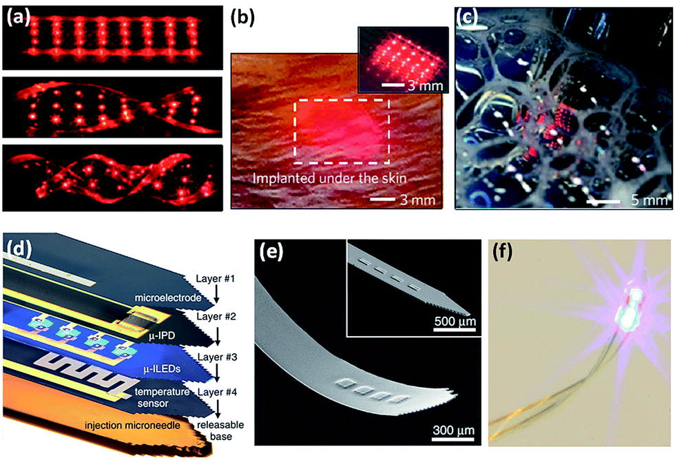 | ||
| Fig. 1 (a) Optical images of an array of micro LEDs on polydimethylsiloxane (PDMS) twisted to different angles. (b) Light-emitting suture on a thread (diameter ∼ 700 μm) in an animal model with a conventional suture needle. (c) Stretchable optical proximity sensor made of an array LEDs and photodetectors mounted on the fingertip of a glove after immersion into soapy water. (d) An injectable cellular-scale optoelectronic device consists of various components. (e) SEM images of the injectable array of LEDs with total thickness of 8.5 μm. (f) Photograph of the integrated system emitting blue light. Adapted with permission from ref. 28 (a–c), and from ref. 34 (d–f), respectively. | ||
Fabrication of flexible devices from conventional thin films is quite challenging and requires additional processing steps to micro-structure the active layers. Moreover, the emission wavelengths are shifting with the bending radii due to the strain induced shifts of the bandgap.23,29 To overcome these issues and further improve the flexibility, it is advantageous to shrink the active element dimensions and to use bottom-up nanostructures. For example, flexibles LEDs based on transferred bottom-up micro-pyramid arrays were demonstrated.35 The transfer was facilitated by formation of nano-voids at the hetero-interface with the substrate. In this study, the micro-pyramid diameter was close to tens of microns. Following this approach, even smaller active elements can be used, such as bottom-up nanowires.
Flexible LEDs based on inorganic bottom-up nanowires
Nanowires show remarkable mechanical and optoelectronic properties stemming from their anisotropic geometry, high surface-to-volume ratio, and crystalline perfection. They are mechanically flexible and can stand high deformations without plastic relaxation,36 which paves the way for their incorporation into flexible devices.Nanowires reduce the lattice matching requirement existing in conventional thin film growth thanks to the strain relaxation by their free lateral surface.37 For light emitting devices, the nanowires also offer their wave guiding properties to facilitate light extraction.38 The bottom-up synthesis of nanowires provides a good control over the morphology, doping and material composition, and in particular allows to grow the active layers in either axial or radial directions. Radial heterostructures present the advantage for LEDs since they increase the active area and thus reduce the current density.39 Finally, availability of compound semiconductors enables bandgap engineering and allows the realization of nanowire LEDs of any color of the visible spectrum. Therefore, nanowires offer an elegant solution to create flexible optoelectronic devices, which combine the high efficiency and the long lifetime of inorganic semiconductor materials with the high flexibility of polymers.
Direct nanowire growth on flexible substrates
One straightforward method of nanowire integration into flexible devices is to grow wires directly on flexible substrates, followed by encapsulation in an insulating polymer layer. This method can be applied to several semiconductor materials, e.g. ZnO nanostructures can be grown in solution on any substrates at low temperature.40 ZnO nanowire arrays grown directly on a flexible substrate have been used to demonstrate LEDs with a broad visible emission band. In 2008, Nadarajah et al.41 reported single-crystalline ZnO nanowires grown on flexible polymer-based indium-tin-oxide (ITO) substrates and then encapsulated in a polystyrene film and top-contacted by a highly-doped polymer covered with an Au film (Fig. 2a and b). The nanowires were used for electron injection while the polystyrene film provided holes. The device showed electroluminescence over almost the whole visible spectrum at a moderate forward bias.41 Similar approach has been applied to fabricate a piezo-phototronic pressure mapping sensor matrix based on ZnO nanowire/p-polymer LED array.42 Another configuration with ZnO nanorods grown on a conductive polymer coated plastic substrate, acting as the back electrode, has been developed as a fully flexible white LED.43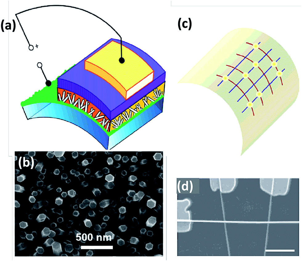 | ||
| Fig. 2 (a) Illustration of a flexible LED structure fabricated on an as-grown substrate with ITO and p-type polymer serving as back and top contacts respectively. (b) ZnO nanowires grown in electrodeposition on a planar transparent substrate as mentioned in (a). (c) Design scheme of a LED display on plastic consisting of a crossed-nanowire array. (d) SEM image of two p-type Si nanowires crossed with an n-type GaN nanowire to form two LEDs. Adapted with permission from ref. 41 (a and b), and from ref. 53 (c and d), respectively. | ||
The direct growth of nanowires on flexible materials eases the process of integration, however, it is limited to few kinds of semiconductors. For plastic substrates, the restriction mainly comes from the limited thermal budget that can be tolerated. Therefore, this approach is mainly limited to growth in solution like electrodeposition44 or hydrothermal deposition.45 There have been also studies of a direct nanowire growth on metal foils by MBE (e.g. GaN nanowires on Ti46 or Ta47). Recently, AlGaN nanowire flexible LEDs grown directly on a flexible Ta foil were demonstrated.47
In-plane transferred nanowire LEDs
As an alternative to the direct growth, one can transfer nanowires to a flexible substrate to form either in-plane or vertical devices. Regarding in-plane transfer, mass-produced n-type ZnO nanowires were roller-pressed on a flexible substrate coated with a p-type organic semiconductors layer and a hole-injection layer (PEDOT:PSS) to form a simple hybrid LED.48 Furthermore, the advances in the alignment of dispersed nanowires with the assistance of electric field,49 magnetic field,50 fluid flow,51 capillary force52 and so on offer new opportunities for the bottom-up approach to nanoelectronics. As shown in Fig. 2c and d, Lieber et al.53 demonstrated a crossed-nanowire ultraviolet LED assembled from n-type GaN NWs and p-type Si NWs, which are sequentially dispersed on a plastic substrate through the orthogonal fluid-directed assembly. This nanowire LED maintains its emissive property after multiple bending cycles.53 However, the complexity in positioning single nanowires and the integration with nonconventional substrates restrict the widespread application of in-plane nanowire LEDs.Vertical transferred nanowire LEDs
Nanowire arrays can also be transferred to flexible substrates preserving their vertical orientation. Nanowire arrays embedded in a flexible film and lifted-off from their native substrate can sustain large deformations thanks to the high flexibility of individual nanowires and to their footprint much smaller than the typical bending curvature radius.54–57 Moreover, the lift-off and transfer procedure enables the assembly of free-standing layers of nanowire materials with different bandgaps without any constraint related to lattice-matching or growth conditions compatibility. This concept therefore allows for a large design freedom and modularity since it enables combination of materials with very different physical and chemical properties, which overcomes the limitations of monolithic growth.Fabrication
A typical process flow to produce flexible devices is the following.58 First, the nanowire array is embedded into a polymer (PDMS) layer. Plasma etching is used to expose and clean the top of the nanowires. Then, the whole layer is peeled off to form a composite membrane with nanowires maintaining their orientation and positions as illustrated in Fig. 3a and e. Two types of devices can be fabricated following this protocol: semitransparent LEDs (Fig. 3a–d) and fully transparent LEDs (Fig. 3e–h). In the case of a semitransparent device, the membrane is flipped onto an arbitrary receiver for the metallization of the nanowire bottom part. After that, a flexible substrate (e.g. PET or metal foil) is brought in contact with the backside metal layer which is mounted using silver epoxy. The top transparent electrode consists of spin-coated Ag nanowires (Fig. 3c). With this method, vertical nanowire array LEDs were fabricated on a copper tape as shown in Fig. 3d. For the fully transparent devices, Ag nanowires are used for both back and top contacts. Fig. 3f shows a flexible membrane back-contacted with Ag nanowires and further encapsulated with another PDMS capping layer for backside electrical insulation and supporting. Ag nanowire coating is then applied on the front side of the layer, as illustrated in Fig. 3g. The full device is displayed in Fig. 3h, which shows a good transparency except for the metallic tape cross for the back contacting. | ||
| Fig. 3 Schematic of the fabrication process flow of flexible LEDs based on vertical nitride nanowire arrays. Panels (a–c) illustrate the fabrication steps for semitransparent LEDs with Ti/Au and Ag nanowires as the back and top contacts, respectively. (d) Photograph of a semitransparent LED. Panels (e–g) show the process of fully transparent LEDs with Ag nanowires as both back and top contacts. (h) Photograph of a transparent LED. Adapted with permission from ref. 58. | ||
It should be noted, that new functionalities can be added to the device by stacking several layers with different functions or by modifying the polymer layer. In particular, PDMS can be doped with YAG:Ce phosphors to down-convert blue light and realize a flexible white nanowire LED.59
Blue and green flexible nanowire LEDs
There have been several reports on light emitters based on polymer-embedded nanowire arrays, where active nanowire components are first embedded in a flexible film and then lifted-off from their native substrate.58–61 The works mainly focus on nitride materials. In all these realizations, the polymer only acted as a mechanical support while the active p–n junction was located in the nanowires. First realizations used GaN p–n junction micro-rods60 and p-GaN/n-ZnO coaxial nanorod heterostructures61 synthesized on graphene films, which acted as back contacts. As shown in Fig. 4, active nanorods grown on graphene-covered Si/SiO2 substrate are encapsulated in an insulating polymer layer. Then a lift-off process of the nanorods embedded in a polymer layer is realized by wet etching of the Si/SiO2 substrate. Finally, the whole layer is transferred onto a metal coated flexible substrate.61 In these realizations, a Ni/Au semi-transparent conductive layer was used as a top electrode, but the low transmittance of this layer is detrimental for light extraction.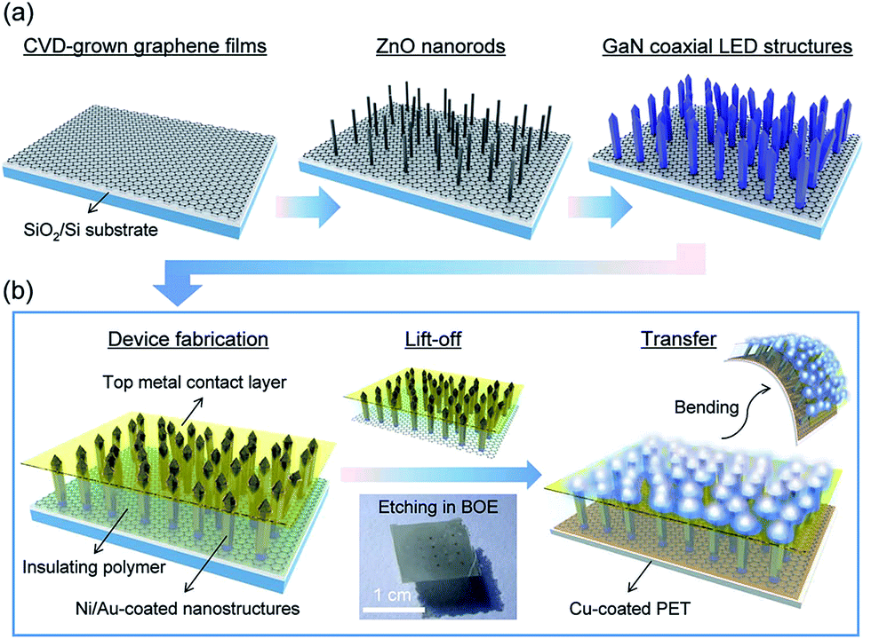 | ||
| Fig. 4 Schematic illustration of the process used to fabricate flexible LEDs using GaN/ZnO coaxial nanorod heterostructures grown on graphene films. Adapted with permission from ref. 61. | ||
Later, flexible LEDs were fabricated using coaxial p–n junction nanowires containing InGaN/GaN quantum wells with a different In content to tune the emission color from blue to green (Fig. 5).58 LEDs present a typical diode current–voltage characteristic with a turn-on voltage around 3 V, corresponding to the appearance of the electroluminescence (EL) (cf.Fig. 5d). The voltage-dependent EL spectra (shown in inset to Fig. 5d) present two peaks at 447 nm and 415 nm with an intensity varying with bias, which are attributed to the spectral contribution of axial and radial QWs.62 At low voltage, the injection current preferentially goes through the nanowire tips into axial QWs where the In-rich region located.62–64 Because of the non-negligible resistance of the p-doped GaN shell, at high injection the hole transport in the shell toward the axial QWs leads to a potential drop and becomes unfavorable.64 The injection takes place under the contact thus favoring the emission from the radial QWs.62 Consequently, the EL peak at shorter wavelength becomes more evident and a broad emission covering the 400–500 nm range is detected. Similar phenomenon has been observed in previous realizations of flexible LEDs based on GaN micro-rods.60
 | ||
| Fig. 5 Mechanical properties of the flexible LED based on vertical nanowire arrays. Photographs of the LED emitting blue light at curvature radii of (a) ∞, (b) 3.5 mm, and (c) −2.5 mm. (d) I–V characteristic of the flexible LED normalized to the number of contacted nanowires (left scale) or to the device surface (right scale). Inset shows the room-temperature EL spectra at various applied biases from 4 V to 8 V. Adapted with permission from ref. 58. | ||
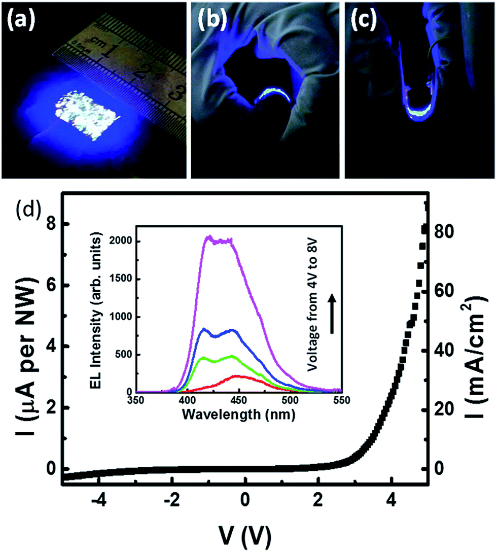
Possible degradation of the LED after bending has been evaluated. Fig. 5a–c show images of LEDs in operation under different bending conditions. No degradation of the I–V curve and of the EL intensity has been found after 10 bending cycles, which suggests a good electrical reliability of the meshed Ag nanowire networks. In addition, no appreciable change in the EL characteristics has been noticed after storage in ambient conditions for more than 30 days.58 Quantitative evaluation of the impact of bending on the properties of flexible LEDs based on ZnO/GaN/InGaN nanowires has been conducted by Lee et al.61Fig. 6a shows EL spectra obtained at different bending radii. There is no significant change in the emission peak wavelength and intensity, suggesting a good reliability of flexible nanowire LEDs even under large bending curvature.
 | ||
| Fig. 6 (a) EL spectra as a function of the bending radius. (b) Integrated emission intensities as a function of bending cycle. Inset shows the EL spectra at different bending cycles. Adapted with permission from ref. 61. | ||
The constant peak position implies that the active regions in individual nanostructures are not under strain because strain generally induces a shift of the emission wavelength as observed in thin film flexible LEDs. Fig. 6b presents the evolution of the device after 100 bending cycles, showing almost identical integrated EL intensity and spectra at a fixed current.
Two-color nanowire flexible LEDs
Taking advantages of the above-mentioned design modularity, multi-layer flexible nanowire LEDs can be achieved by stacking fully transparent LEDs of different colors.58 The assembly of nanowire materials with different emission wavelengths is a prerequisite for flexible display applications. Fig. 7a illustrates a vertically integrated device consisting of two layers of nanowire LEDs with emission wavelengths in the blue and green, respectively. The nanowires are contacted with transparent electrodes and assembled on a flexible substrate with an intermediate PDMS layer. The EL spectra of this two-layer device under different biasing conditions are shown in Fig. 7b. Independent voltage sources V1 and V2 are connected to the top and bottom layers.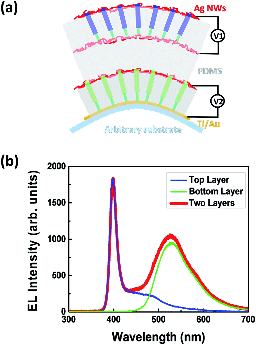 | ||
| Fig. 7 (a) Schematic of a 2-color nanowire flexible LED. (b) EL spectra of a two-layer flexible LED with a top transparent layer and a bottom semi-transparent layer. Adapted with permission from ref. 58. | ||
By biasing the top LED, the bottom LED or both LEDs simultaneously, different spectra are obtained as shown in Fig. 7b. The optical transmittance of the top transparent LED layer is above 60% in the green spectral range and allows for an efficient extraction of the green luminescence of the bottom layer. As a result, the feasibility of multi-layer flexible LEDs by a mechanical stacking technique is demonstrated with no limitations for the number of layers except for the residual absorption. Such configuration enables the vertical integration of nanowire layers of different semiconductor materials (e.g. nitrides with phosphides or arsenides) as well as a hybrid integration of blue inorganic LED with organic LEDs to achieve RGB emission and white LEDs.
White nanowire flexible LEDs
A vertical integration of red, green and blue LEDs allows for the realization of white LEDs, however, it requires a careful balance between colors in order to achieve a stable white light. Alternatively, a white LED can be achieved by combining a blue nitride LED and yellow phosphors, down-converting a part of the blue light. Recently, a rigid white nanowire LED has been demonstrated by combining blue nanowire LEDs with phosphor down conversion.65 The same principle can be applied to flexible white LEDs by doping the encapsulating PDMS layer with YAG:Ce nanophosphors (Fig. 8a).59 White LED emits a broad spectrum from 400 to 700 nm. The XYZ tristimulus values of the Commission International de l'Eclairage (CIE) 1931 is estimated from the EL spectrum. As shown in Fig. 8b, the LED color locates at x = 0.3011, y = 0.4688 corresponding to a cool-white light with a correlated color temperature (CCT) of 6306 K and with a color rendering index (CRI) of 54. Fig. 8d–f presents photographs of the white LED under different bending conditions. Based on the measured emission power, EQE is calculated as a function of the injection current density. The maximum EQE of 9.3% is obtained at a current density of 14.6 A cm−2, after which a droop is observed. | ||
| Fig. 8 (a) Schematic of the flexible white LED. (b) CIE 1931 chromaticity diagram of flexible white LEDs under injection current density of 3.9 A cm−2 (chromaticity coordinates x = 0.3011, y = 0.4688; CCT = 6306 K; CRI = 54). (c) Room temperature EQE deduced from the measured optical power versus the injection current density. (d–f) Photographs of the operating flexible white LED with bending radii of infinity, 5 mm, and −5 mm, respectively. Adapted with permission from ref. 59. | ||
Conclusions and perspectives
In conclusion, to break through the limitations of opto-electronic stability, efficiency and lifetime of OLEDs, many efforts are dedicated to inorganic semiconductor flexible LEDs by micro-transfer printing of conventional thin film LEDs and micro-pyramid array LEDs. As an elegant alternative, bottom-up nanowire LEDs can be used as the active material for flexible LEDs. This technology combines the high efficiency of III–V semiconductors and the mechanical flexibility of nanowires and of the flexible substrates. Different LED architectures were proposed for flexible nanowire LEDs. The most promising appears to be the vertical transferred configuration. Blue, green, white flexible LEDs as well as a blue-green bi-color flexible LED were demonstrated using this concept. These devices are characterized by a good flexibility, reliability and time stability. The large design freedom and modularity offered by free-standing nanowire/polymer membranes provide the possibility to integrate materials with different physical and chemical properties. In particular, this opens new possibilities for efficient flexible LED displays. Other nanowire-based flexible devices can also be realized with this strategy, e.g., photodetectors,66 solar cells, piezoelectric generators, etc.Conflicts of interest
There are no conflicts of interest to declare.Acknowledgements
This work has been financially supported by ANR-14-CE26-0020-01 project “PLATOFIL”, EU H2020 ERC project “NanoHarvest” (grant no. 639052) and French national Labex GaNex (ANR-11-LABX-2014). A. Babichev acknowledges the support of RFBR (project no. 15-02-08282 A), program of fundamental research of the Presidium of the RAS No. 1 (project no. 1.3.3.3).Notes and references
- C. W. Tang and S. A. Vanslyke, Appl. Phys. Lett., 1987, 51, 913 CrossRef CAS.
- D. Y. Kondakov, W. C. Lenhart and W. F. Nichols, J. Appl. Phys., 2007, 101, 024512 CrossRef.
- Y. Zhang and H. Aziz, ACS Appl. Mater. Interfaces, 2017, 9, 636 CAS.
- S. Scholz, D. Kondakov, B. Lüssem and K. Leo, Chem. Rev., 2015, 115, 8449 CrossRef CAS PubMed.
- N. Thejokalyani and S. J. Dhoble, Renewable Sustainable Energy Rev., 2014, 32, 448 CrossRef CAS.
- Organic Light-Emitting Materials and Devices, ed. Z. Li, CRC Press, New York, 2nd edn, 2015, vol. 3 Search PubMed.
- C. W. Lee and J. Y. Lee, Adv. Mater., 2013, 25, 5450 CrossRef CAS PubMed.
- Y. Zhang, J. Lee and S. R. Forrest, Nat. Commun., 2014, 5, 5008 CrossRef CAS PubMed.
- A. Fallahi, F. A. Taromi, A. Mohebbi, J. D. Yuen and M. Shahinpoor, J. Mater. Chem. C, 2014, 2, 6491 RSC.
- T. Tsujimura in OLED Display Fundamentals and Applications, John Wiley & Sons, Inc., New Jersey, 2017, ch. 2, p. 7, DOI:10.1002/9781119187493.ch2.
- J. Herrnsdorf, J. J. D. McKendry, S. Zhang, E. Xie, R. Ferreira, D. Massoubre, A. M. Zuhdi, R. K. Henderson, I. Underwood, S. Watson, A. E. Kelly, E. Gu and M. D. Dawson, IEEE Trans. Electron Devices, 2015, 62, 1918 CrossRef CAS.
- H. X. Jiang and J. Y. Lin, Opt. Express, 2013, 21, A475 CrossRef CAS PubMed.
- Y. Narukawa, M. Ichikawa, D. Sanga, M. Sano and T. Mukai, J. Phys. D: Appl. Phys., 2010, 43, 354002 CrossRef.
- S. Nakamura, Rev. Mod. Phys., 2015, 87, 1139 CrossRef CAS.
- M. H. Chang, D. Das, P. V. Varde and M. Pecht, Microelectron. Reliab., 2012, 52, 762 CrossRef.
- J. Yoon, S.-M. Lee, D. Kang, M. A. Meitl, C. A. Bower and J. A. Rogers, Adv. Opt. Mater., 2015, 3, 1313 CrossRef CAS.
- L. Wang, J. Ma, Z. Liu, X. Yi, H. Zhu and G. Wang, ACS Photonics, 2014, 1, 421 CrossRef CAS.
- S. H. Lee, S. Y. Park and K. J. Lee, Proc. SPIE, 2012, 8460, 846011 CrossRef.
- C. Goßler, C. Bierbrauer, R. Moser, M. Kunzer, K. Holc, W. Pletschen, K. Köhler, J. Wagner, M. Schwaerzle, P. Ruther, O. Paul, J. Neef, D. Keppeler, G. Hoch, T. Moser and U. T. Schwarz, J. Phys. D: Appl. Phys., 2014, 47, 205401 CrossRef.
- J.-H. Seo, J. Li, J. Lee, S. Gong, J. Lin, H. Jiang and Z. Ma, IEEE Photonics J., 2015, 7, 1 CrossRef CAS.
- P. Tian, J. J. D. McKendry, E. Gu, Z. Chen, Y. Sun, G. Zhang, M. D. Dawson and R. Liu, Opt. Express, 2016, 24, 699 CrossRef CAS PubMed.
- C.-W. Cheng, K.-T. Shiu, N. Li, S.-J. Han, L. Shi and D. K. Sadana, Nat. Commun., 2013, 4, 1577 CrossRef PubMed.
- C.-H. Cheng, T.-W. Huang, C.-L. Wu, M. K. Chen, C. H. Chu, Y.-R. Wu, M.-H. Shih, C.-K. Lee, H.-C. Kuo, D. P. Tsai and G.-R. Lin, J. Mater. Chem. C, 2017, 5, 607 RSC.
- C. K. Jeong, K.-I. Park, J. H. Son, G.-T. Hwang, S. H. Lee, D. Y. Park, H. E. Lee, H. K. Lee, M. Byun and K. J. Lee, Energy Environ. Sci., 2014, 7, 4035 CAS.
- K. Chung, C.-H. Lee and G.-C. Yi, Science, 2010, 330, 655 CrossRef CAS PubMed.
- Y. Kobayashi, K. Kumakura, T. Akasaka and T. Makimoto, Nature, 2012, 484, 223 CrossRef CAS PubMed.
- S.-I. Park, Y. Xiong, R.-H. Kim, P. Elvikis, M. Meitl, D.-H. Kim, J. Wu, J. Yoon, C.-J. Yu, Z. Liu, Y. Huang, K.-C. Hwang, P. Ferreira, X. Li, K. Choquette and J. A. Rogers, Science, 2009, 325, 977 CrossRef CAS PubMed.
- R.-H. Kim, D.-H. Kim, J. Xiao, B. H. Kim, S.-I. Park, B. Panilaitis, R. Ghaffari, J. Yao, M. Li, Z. Liu, V. Malyarchuk, D. G. Kim, A.-P. Le, R. G. Nuzzo, D. L. Kaplan, F. G. Omenetto, Y. Huang, Z. Kang and J. A. Rogers, Nat. Mater., 2010, 9, 929 CrossRef CAS PubMed.
- S.-I. Park, A.-P. Le, J. Wu, Y. Huang, X. Li and J. A. Rogers, Adv. Mater., 2010, 22, 3062 CrossRef CAS PubMed.
- K. Lee, J. D. Zimmerman, T. W. Hughes and S. R. Forrest, Adv. Funct. Mater., 2014, 24, 4284 CrossRef CAS.
- H.-S. Kim, E. Brueckner, J. Song, Y. Li, S. Kim, C. Lu, J. Sulkin, K. Choquette, Y. Huang, R. G. Nuzzo and J. A. Rogers, Proc. Natl. Acad. Sci. U. S. A., 2011, 108, 10072 CrossRef CAS PubMed.
- J. Chun, Y. Hwang, Y.-S. Choi, T. Jeong, J. H. Baek, H. C. Ko and S.-J. Park, IEEE Photonics Technol. Lett., 2012, 24, 2115 CrossRef CAS.
- S. Y. Lee, K.-I. Park, C. Huh, M. Koo, H. G. Yoo, S. Kim, C. S. Ah, G. Y. Sung and K. J. Lee, Nano Energy, 2012, 1, 145 CrossRef CAS.
- T.-I. Kim, J. G. Mccall, Y. H. Jung, X. Huang, E. R. Siuda, Y. Li, J. Song, Y. M. Song, H. A. Pao, R.-H. Kim, C. Lu, S. D. Lee, I.-S. Song, G. Shin, R. Al-Hasani, S. Kim, M. P. Tan, Y. Huang, F. G. Omenetto, J. A. Rogers and M. R. Bruchas, Science, 2013, 340, 211 CrossRef CAS PubMed.
- J. H. Choi, E. H. Cho, Y. S. Lee, M.-B. Shim, H. Y. Ahn, C.-W. Baik, E. H. Lee, K. Kim, T.-H. Kim, S. Kim, K.-S. Cho, J. Yoon, M. Kim and S. Hwang, Adv. Opt. Mater., 2013, 2, 267 CrossRef.
- H. D. Espinosa, R. A. Bernal and M. Minary-Jolandan, Adv. Mater., 2012, 24, 4656 CrossRef CAS PubMed.
- F. Glas, Phys. Rev. B: Condens. Matter Mater. Phys., 2006, 74, 121302 CrossRef.
- J. Chesin and S. Gradecak, J. Nanophotonics, 2014, 8, 083095 CrossRef.
- S. Li and A. Waag, J. Appl. Phys., 2012, 111, 071101 CrossRef.
- M. Willander, O. Nur, Q. X. Zhao, L. L. Yang, M. Lorenz, B. Q. Cao, J. Z. Pérez, C. Czekalla, G. Zimmermann, M. Grundmann, A. Bakin, A. Behrends, M. Al-Suleiman, A. El-Shaer, A. C. Mofor, B. Postels, A. Waag, N. Boukos, A. Travlos, H. S. Kwack, J. Guinard and D. L. S. Dang, Nanotechnology, 2009, 20, 332001 CrossRef CAS PubMed.
- A. Nadarajah, R. C. Word, J. Meiss and R. Könenkamp, Nano Lett., 2008, 8, 534 CrossRef CAS PubMed.
- R. Bao, C. Wang, L. Dong, R. Yu, K. Zhao, Z. L. Wang and C. Pan, Adv. Funct. Mater., 2015, 25, 2884 CrossRef CAS.
- N. Bano, S. Zaman, A. Zainelabdin, S. Hussain, I. Hussain, O. Nur and M. Willander, J. Appl. Phys., 2010, 108, 043103 CrossRef.
- H. Guo, J. Zhou and Z. Lin, Electrochem. Commun., 2008, 10, 146 CrossRef CAS.
- M. Guo, P. Diao and S. Cai, J. Solid State Chem., 2005, 178, 1864 CrossRef CAS.
- G. Calabrese, P. Corfdir, G. Gao, C. Pfüller, A. Trampert, O. Brandt, L. Geelhaar and S. Fernández-Garrido, Appl. Phys. Lett., 2016, 108, 202101 CrossRef.
- B. J. May, A. T. M. G. Sarwar and R. C. Myers, Appl. Phys. Lett., 2016, 108, 141103 CrossRef.
- J. Liu, Y. H. Ahn, J.-Y. Park, K. H. Koh and S. Lee, Nanotechnology, 2009, 20, 445203 CrossRef PubMed.
- C. S. Lao, J. Liu, P. Gao, L. Zhang, D. Davidovic, R. Tummala and Z. L. Wang, Nano Lett., 2006, 6, 263 CrossRef CAS PubMed.
- M. Tanase, L. A. Bauer, A. Hultgren, D. M. Silevitch, L. Sun, D. H. Reich, P. C. Searson and G. J. Meyer, Nano Lett., 2001, 1, 155 CrossRef CAS.
- E. M. Freer, O. Grachev and D. P. Stumbo, Nat. Nanotechnol., 2010, 5, 525 CrossRef CAS PubMed.
- X. Zhou, Y. Zhou, J. C. Ku, C. Zhang and C. A. Mirkin, ACS Nano, 2014, 8, 1511 CrossRef CAS PubMed.
- M. C. Mcalpine, R. S. Friedman, S. Jin, K.-H. Lin, W. U. Wang and C. M. Lieber, Nano Lett., 2003, 3, 1531 CrossRef CAS.
- Z. Fan, H. Razavi, J.-W. Do, A. Moriwaki, O. Ergen, Y.-L. Chueh, P. W. Leu, J. C. Ho, T. Takahashi, L. A. Reichertz, S. Neale, K. Yu, M. Wu, J. W. Ager and A. Javey, Nat. Mater., 2009, 8, 648 CrossRef CAS PubMed.
- J. M. Spurgeon, S. W. Boettcher, M. D. Kelzenberg, B. S. Brunschwig, H. A. Atwater and N. S. Lewis, Adv. Mater., 2010, 22, 3277 CrossRef CAS PubMed.
- K. E. Plass, M. A. Filler, J. M. Spurgeon, B. M. Kayes, S. Maldonado, B. S. Brunschwig, H. A. Atwater and N. S. Lewis, Adv. Mater., 2009, 21, 325 CrossRef CAS.
- M. E. Reimer, G. Bulgarini, N. Akopian, M. Hocevar, M. B. Bavinck, M. A. Verheijen, E. P. Bakkers, L. P. Kouwenhoven and V. Zwiller, Nat. Commun., 2012, 3, 737 CrossRef PubMed.
- X. Dai, A. Messanvi, H. Zhang, C. Durand, J. Eymery, C. Bougerol, F. H. Julien and M. Tchernycheva, Nano Lett., 2015, 15, 6958 CrossRef PubMed.
- N. Guan, X. Dai, A. Messanvi, H. Zhang, J. Yan, E. Gautier, C. Bougerol, F. H. Julien, C. Durand, J. Eymery and M. Tchernycheva, ACS Photonics, 2016, 3, 597 CrossRef CAS PubMed.
- K. Chung, H. Beak, Y. Tchoe, H. Oh, H. Yoo, M. Kim and G.-C. Yi, APL Mater., 2014, 2, 092512 CrossRef.
- C.-H. Lee, Y.-J. Kim, Y. J. Hong, S.-R. Jeon, S. Bae, B. H. Hong and G.-C. Yi, Adv. Mater., 2011, 23, 4614 CrossRef CAS PubMed.
- G. Jacopin, A. D. L. Bugallo, P. Lavenus, L. Rigutti, F. H. Julien, L. F. Zagonel, M. Kociak, C. Durand, D. Salomon, X. J. Chen, J. Eymery and M. Tchernycheva, Appl. Phys. Express, 2011, 5, 014101 CrossRef.
- Y. J. Hong, C.-H. Lee, A. Yoon, M. Kim, H.-K. Seong, H. J. Chung, C. Sone, Y. J. Park and G.-C. Yi, Adv. Mater., 2011, 23, 3284 CrossRef CAS PubMed.
- M. Tchernycheva, P. Lavenus, H. Zhang, A. V. Babichev, G. Jacopin, M. Shahmohammadi, F. H. Julien, R. Ciechonski, G. Vescovi and O. Kryliouk, Nano Lett., 2014, 14, 2456 CrossRef CAS PubMed.
- T. Schimpke, M. Mandl, I. Stoll, B. Pohl-Klein, D. Bichler, F. Zwaschka, J. Strube-Knyrim, B. Huckenbeck, B. Max, M. Müller, P. Veit, F. Bertram, J. Christen, J. Hartmann, A. Waag, H.-J. Lugauer and M. Strassburg, Phys. Status Solidi A, 2016, 213, 1577 CrossRef CAS.
- H. Zhang, X. Dai, N. Guan, A. Messanvi, V. Neplokh, V. Piazza, M. Vallo, C. Bougerol, F. H. Julien, A. Babichev, N. Cavassilas, M. Bescond, F. Michelini, M. Foldyna, E. Gautier, C. Durand, J. Eymery and M. Tchernycheva, ACS Appl. Mater. Interfaces, 2016, 8, 26198 CAS.
| This journal is © The Royal Society of Chemistry 2017 |