
 Open Access Article
 This Open Access Article is licensed under a
 Creative Commons Attribution 3.0 Unported Licence
Metal halide perovskite nanomaterials: synthesis and applications
Son-Tung
Ha
a,
Rui
Su
a,
Jun
Xing
a,
Qing
Zhang
c and
Qihua
Xiong
*ab
aDivision of Physics and Applied Physics, School of Physical and Mathematical Sciences, Nanyang Technological University, Singapore 637371. E-mail: Qihua@ntu.edu.sg
bNOVITAS, Nanoelectronics Centre of Excellence, School of Electrical and Electronic Engineering, Nanyang Technological University, Singapore 639798
cDepartment of Materials Science and Engineering, College of Engineering, Peking University, Beijing 100871, P. R. China
First published on 16th December 2016
Abstract
Nanomaterials refer to those with at least one dimension being at the nanoscale (i.e. <100 nm) such as quantum dots, nanowires, and nanoplatelets. These types of materials normally exhibit optical and electrical properties distinct from their bulk counterparts due to quantum confinement or strong anisotropy. In this perspective, we will focus on a particular material family: metal halide perovskites, which have received tremendous interest recently in photovoltaics and diverse photonic and optoelectronic applications. The different synthesis approaches and growth mechanisms will be discussed along with their novel characteristics and applications. Taking perovskite quantum dots as an example, the quantum confinement effect and high external quantum efficiency are among these novel properties and their excellent performance in applications, such as single photon emitters and LEDs, will be discussed. Understanding the mechanism behind the formation of these nanomaterial forms of perovskite will help researchers to come up with effective strategies to combat the emerging challenges of this family of materials, such as stability under ambient conditions and toxicity, towards next generation applications in photovoltaics and optoelectronics.
1. Introduction
Nanomaterial research is one of the most important branches in modern physics where many quantum physics theories are experimented and validated. For instance, semiconductor quantum dots exhibit excellent exciton confinement and a near unity external quantum yield of photoluminescence. Another example is carbon nanotubes, which are an ideal quantum wire system for physicists to study electronic confinement in one dimension. In 2004, Andre Geim and Konstantin Novoselov, who were later awarded the Nobel Prize in Physics in 2010, experimentally isolated graphene – a single layer of hexagonal-structured carbon atoms.1 The discovery of this truly two dimensional (2D) material blasted a new wave in research at the global scale, leading the low dimensional materials to their “golden age”. Since then, many other families of 2D materials have been explored, such as boron nitride,2,3 transition metal dichalcogenide (TMD),4–7 and black phosphorus.8,9So what are the properties that set aside nanomaterials from their bulk counterparts? First of all, when a material has one or more reduced dimensions, it can have a very high surface area to volume ratio. Consequently, the surface state of that material becomes more important and even dominant (e.g. in quantum dots). Moreover, the constraint of dimensionality in semiconductors leads to various quantum size effects, which can significantly change the energy spectrum of electrons and their behavior. In some systems, such as MoS2 and WS2, lowering the number of layers down to a monolayer will change the nature characteristics of the materials from indirect to direct bandgap. In graphene, the quantum mechanical description of the Bloch wave of electrons renders a new kind of quasiparticle, which moves like an electron that has completely lost its mass, following an analogous description of the Dirac equation. These new phenomena that only happen at low dimensionality are responsible for their extraordinary electronic, optical, thermal, mechanical, and chemical properties, which may be applied in a wide range of applications.
Recently, metal halide perovskites have received substantial attention from the research community due to their applications in solar cells,10–12 lasers,13–15 light emitting diodes (LED),16–18 water splitting,19,20 laser cooling21etc. The material is now considered as the most promising material for the future of opto-electronics because of its high performance, low cost, and abundance.22 Lead halide perovskites were firstly used in the dye-sensitized solar cell configuration in 2009 by Miyasaka and colleagues with an initial efficiency of only 3.8%,23 and were later employed in the all-solid configuration in 2012 by Kim et al.24 Since then, the performance of perovskite solar cells has been dramatically improved mostly by material and interface engineering, which boosted the efficiency over 20%.25 The perovskite material exhibits excellent optical and electrical properties, such as a high absorption coefficient, strong photoluminescence, low trap-state density, and long carrier diffusion length.13,26–28 Even though organic–inorganic hybrid perovskites have been synthesized and known for over 100 years, the first study of electrical properties for tin-based perovskite was reported by Mitzi et al. in 1994 as a new family of semiconductor materials.29 After that, the perovskites have been used in various forms of devices, such as field effect transistors (FETs), and LEDs with limited performance.30–32 The attention towards this material was only raised again when it was applied in a solar cell in 2009,23 which later turned out to be one of the most effective light absorber materials for solar cells to date.
Metal halide perovskites are mainly classified into two categories based on their crystal structure motif. The first one is called a 3D-structured perovskite with the general chemical formula AMX3 and the other is called a 2D-structured or layered perovskite with the formula A2MX4, where M is a divalent metal (such as Pb or Sn), X is a halide (Cl, Br, or I), and A is a cation which can be inorganic (e.g. Cs+) or organic (e.g. CH3NH3+, C4H9NH3+, C6H5–C2H4NH2+, etc.). We should not be confused by the term 3D and 2D here, which are related to the structural motifs of the material while the other 0D–3D refer to the dimensions of materials. The term “perovskite” originated from the similarity in crystal structure of the material to the perovskite crystal CaTiO3. In this case, the divalent metal M is surrounded by six halogen atoms in an octahedral structure, and the cation A is either located in the center of an eight MX6 octahedral network (in the case of 3D perovskite) or sandwiched between corner-sharing MX6 octahedral layers (in 2D perovskite) as illustrated in Fig. 1.33 Due to its natural layered structure, where each layer of MX6 octahedra is only connected to each other by a weak van der Waals force, the 2D-structured perovskites are much easier to prepare in the 2D form, either by mechanical exfoliation or a chemical method. Indeed, Dou et al. has reported large scale synthesis of monolayer (C4H9NH3)2PbBr4 by a chemical method.34 Many other efforts have been made to prepare and characterize nanomaterial forms of the perovskites.35–38 In our group, we have prepared nanoplatelets and nanowires of perovskites by vapor phase synthesis to realize their excellent natural cavity in optical lasing.14,39–41 The high crystallinity and optical quality of the nanoplatelets also enabled the experimental demonstration of laser cooling in the perovskite material.21 The high external quantum efficiency of colloidal quantum dots of perovskites further boosted their performance in LEDs.17,42 Recently, the idea of hetero-structuring perovskite 2D sheets and other 2D materials, such as graphene or TMD, is becoming an interesting concept for integrating this material into low dimensional optoelectronics.
 | ||
| Fig. 1 Structure of 3D and 2D perovskites:33 (a) structure of AMX3 3D perovskite; (b) structure of layered perovskites with (left) monoammonium (RNH3+) or (right) diammonium (+H3N–R-NH3+) organic cations. | ||
In this perspective, we aim at presenting recent breakthroughs in the preparation and characterization of metal halide perovskite nanomaterials (i.e. quantum dots, nanowires, and nanoplatelets). In the following sections, we would like to start from the synthesis of each type of perovskite nanomaterial, since this may be the first obstacle for any extensive material research to be made. We will review both chemical and physical methods and discuss their advantages as well as disadvantages. We will also discuss the growth mechanism to understand the formation of the material in its nanosized forms. Next, we will discuss their novel optical, electronic properties and their applications in various optoelectronic devices. Finally, we conclude the whole area and provide an outlook for the future development of these materials.
2. Synthesis and growth mechanism of metal halide perovskite nanomaterials
2.1 Perovskite quantum dots
Organic–inorganic perovskite colloidal nanoparticles (NPs) were firstly synthesized by Schmidt et al.43 The NPs were prepared by a simple and reliable method under an ambient atmosphere, in which a DMF solution of CH3NH3Br and PbBr2 reacted and precipitated in an acetone solution in the presence of long chain alkyl ammonium bromide, oleic acid (OLA) and octadecene (ODE). They proposed the growth mechanism as while the methylammonium cations are embedded in the voids of the corner-sharing PbX6 octahedra, the long alkyl chain cations only fit the periphery of the octahedra with their chains dangling outside it. Thus, these ammonium ions would act as the capping ligands to limit the growth of the colloidal NPs extending in three dimensions. The XRD patterns showed a cubic phase of the MAPbBr3 NPs and the HRTEM images showed the spherical morphology of the NPs with an average size of 6 nm. The MAPbBr3 colloidal NPs exhibited an absorption peak at 525 nm and a PL peak at 527 nm which is blueshifted compared to the absorption peak at 550 nm and PL peak at 570 nm of the MAPbBr3 bulk crystal. The colloidal NPs showed a high PL quantum yield (PLQY) of 20% in toluene and remain stable in a series of aprotic, moderate polarity, organic solvents for more than three months. Next, they further optimized the synthesis of MAPbBr3 colloidal NPs by tuning the ratio of MABr, PbBr, octylammonium bromide (OABr) and ODE.44 Finally, the best colloidal NPs with a particle size of 5.5 nm and PLQY of 83% were obtained by using a larger ratio of the ammonium and PbBr2, but in the absence of OLA.A similar precipitation method was also used to synthesize mixed halide perovskite MAPbX3 colloidal NPs with different Br/I and Br/Cl compositions (Fig. 2).45 The PL spectra of these mixed halide perovskites can be finely tuned from 407 to 734 nm by varying the content of halogen cations and their absolute PLQYs can be reach 50–70%. Typically, MAPbBr3 NPs have an average diameter of 3.3 nm and a PLQY of 70%. The exciton binding energy of MAPbBr3 NPs was calculated to be 375 meV, which is much larger than that of the bulk counterpart of 65 meV. Rogach et al. reported a synthesis of MAPbBr3 NPs with the variation of the temperature of the bad solvent between 0–60 °C.46 The MAPbBr3 NP size can be controlled by the temperature; 1.8 nm, 2.8 nm, and 3.6 nm average diameters were obtained under 0, 30, and 60 °C, respectively. The PL spectra were tuned from 470 nm (0 °C) to 520 nm (60 °C) and the PLQYs of the series colloidal NPs started at 74% for the 0 °C sample and steadily increased, reaching as high as 93% for the 60 °C sample. However, these phenomena are still not enough to confirm the quantum confinement of the perovskite colloidal NPs. That is because the long chain alkyl ammonium was used as ligands to synthesize the perovskite NPs, which might form quasi-2D perovskites with blueshifted PL spectra.47,48 Our group also reported the synthesis of the perovskite MAPbX3 colloidal NPs with emission from 403 to 740 nm.17 However, we used different precursor solutions; DMF and γ-butyrolactone as the solvent, octylamine as ligands and without OLA. Here, the absence of the OLA can keep the colloidal solution more stable, even enabling storage for several months. It can be deduced from the XRD patterns and HRTEM images that the as-synthesized perovskite colloidal NPs exhibit a typical amorphous phase, which is attributed to free PbX6 (X = Br or DMF anion) dispersed in the DMF and γ-butyrolactone mixed solution. When the precursor solution was injected into toluene, PbX6 units would aggregate and reprecipitate, but the crystallization process would be blocked by the octylamine. Notable, the HRTEM was conducted at a low acceleration voltage of 60 kV to exclude the possible recrystallization of the amorphous perovskite under a high acceleration voltage. Although the reprecipitation method is a fast and facile strategy to synthesize highly luminescent MAPbX3 colloidal NPs, the yield of the product is very limited due to the formation of aggregated clusters together with the NPs.
 | ||
| Fig. 2 (a) Schematic illustration of the reaction system and process for the LARP technique and typical optical image of the colloidal MAPbBr3 solution. (b) HRTEM image of MAPbBr3 colloidal NPs. (c) Optical absorption and PL spectra of perovskites with different halide components. (d) Digital image of the perovskite colloidal solutions in toluene under ambient light and an UV lamp, light emission from 438 to 660 nm. Reprinted with permission from ref. 17 and 45, copyright 2015, 2016 American Chemical Society. | ||
 | ||
| Fig. 3 Transmission electron microscopy (TEM) images of ∼10 nm CsPbX3 NCs after treatment with various quantities of (a) chloride and (b) iodide anions. The insets show the evolution of emission colors under an UV lamp. Reprinted with permission from ref. 50, copyright 2015, American Chemical Society. | ||
The high PLQY of perovskite MAPbX3 colloidal NPs motivated the preparation of inorganic CsPbX3 (X = Cl, Br, I, and mixed Cl/Br and Br/I) NPs. Protesescu et al. synthesized CsPbX3 colloidal NPs for the first time by injecting the precursor Cs-oleate into a PbX2 solution containing OLA, OA, trioctylphosphine (TOPO), and ODE at high temperature as in the case of CdS/Se quantum dots.49 The CsPbX3 colloidal NPs exhibited a cubic shape (4–15 nm edge lengths) and cubic perovskite crystal structure. Through compositional modulations and quantum size-effects, the emission spectra are also tunable over the entire visible spectral region of 410–700 nm. The PL of the CsPbX3 NCs shows narrow emission line widths of 12–42 nm (from blue to red) and high PLQYs of 50–90%. Within the effective mass approximation, they estimated the effective Bohr diameters of Wannier–Mott excitons and the binding energies for CsPbCl3 (5 nm, 75 meV), CsPbBr3 (7 nm, 40 meV), and CsPbI3 (12 nm, 20 meV). Nedelcu et al. and Akkerman et al. further observed fast anion exchange in CsPbX3 (X = Cl, Br, I) perovskite NPs at low temperature (Fig. 3).50 By adjusting the halide ratios in the colloidal nanocrystal solution, the bright PL could be tuned over 410–700 nm while maintaining high quantum yields of 20–80% and narrow emission line widths of 10–40 nm. Furthermore, the fast inter-nanocrystal anion-exchange was also demonstrated between the CsPbCl3, CsPbBr3, and CsPbI3 NPs, leading to uniform CsPb(Cl/Br)3 or CsPb(Br/I)3 compositions. After that, there are many reports on CsPbX3 colloidal NPs synthesized based on this methods, but with different crystal phases. For example, Swarnkar et al. synthesized CsPbBr3 colloidal NPs following the above methods, but obtained orthorhombic phase CsPbBr3.51 It should be noted that the colloidal NPs had broader XRD peaks and the cubic and orthorhombic phases exhibited very closed XRD patterns, so it is difficult to distinguish these phases.
Inspired by the methodology for synthesis of perovskite MAPbX3 colloidal NPs, Li et al. extended the supersaturated recrystallization method to inorganic perovskite CsPbX3.52 Although crystallized at RT, these colloidal NPs have superior optical properties to those formed at high temperature, including PLQYs of 80%, 95%, and 70% for red, green, and blue PLs, and a 90% retention rate after aging for 30 days under ambient conditions. Deng et al. used a reprecipitation strategy to systematically manipulate the shape of CsPbX3 colloidal NPs, such as spherical colloidal NPs and nanocubes, by using different ligands.53 De Roo et al. studied the dynamic ligand of the inorganic perovskite CsPbX3.54 They found that compared to classical chalcogenide quantum dots, CsPbX3 is more ionic in nature and the interactions with capping ligands are also more ionic and labile. Therefore, ligand binding to the NP surface is highly dynamic and easily lost during the isolation and purification procedures. However, when a small amount of both oleic acid and oleylamine is added, the NPs can be purified, maintaining optical, colloidal, and material integrity. A high amine content in the ligand shell would increase the quantum yield due to the improved binding of the carboxylic acid. Most recently, Swarnkar et al.55 reported the synthesis of ambient-stable cubic-phase quantum dots of CsPbI3, a phase that was previously known to be stable only at high temperature. They have developed an improved synthetic route and purification approach that prevent the CsPbI3 quantum dots from transforming their as-synthesized cubic phase to orthorhombic. The difference in their method compared to the conventional method is that they used methyl acetate (i.e. antisolvent) to remove excess unreacted precursor without causing agglomeration, resulting in stable cubic CsPbI3 quantum dots. The material has been used to fabricate solar cells and LEDs, which exhibited the highest power conversion efficiency of 10.77% for all-inorganic perovskite solar cells to date.55
2.2 Perovskite nanowires (1D)
As lead halide perovskites have triggered a revolution in photovoltaic solar cells, much effort has been directed to the synthesis of large area lead halide perovskite films due to their excellent optoelectronic properties.11,16,56–61 Nonetheless, lead halide perovskite nanowires are also of great importance due to their novel optical and electronic properties, as well as their potential as building blocks for various applications in optoelectronic devices.15,39,62–65 Over the past few decades, a lot of effort has been spent on the synthesis of II–VI and III–V semiconductor nanowires, which is mainly based on a chemical vapor deposition (CVD) process.66–70 This method is the most widely used approach due to its versatility and simplicity in many semiconductor systems. The CVD process is used to obtain nanowires primarily based on a vapor–liquid–solid (VLS) mechanism, utilizing noble metal films as the catalyst to drive the one dimensional crystal growth. However, this VLS method is rarely adopted in the growth of perovskite nanowires, which could be possibly attributed to the low growth temperature of perovskites.Compared with previous III–VI and II–VI semiconductors based on a VLS mechanism, the facile solution processed synthesis of lead halide perovskites could be the most attracting point for low cost applications.13,27,71–73 Much effort has been devoted to synthesizing lead halide perovskite nanowires by solution methods.15,62,65,74 Large area high quality single crystal methylammonium (MA) lead halide perovskite nanowires were reported in the pioneering work on nanowire lasers by Zhu and his co-workers.15 In this work, no surfactant ligand is used for the controlled anisotropic crystal growth. A lead acetate (PbAc2) solid thin film was firstly deposited on a glass substrate by using a PbAc2·3H2O aqueous solution. This PbAc2 solid film was then immersed in a CH3NH3X (X = I, Br, Cl or mix halide precursors) solution in isopropanol in an ambient environment for over 20 h. Consequently, high quality methylammonium lead halide perovskite nanowires were obtained with lengths up to 20 μm and flat rectangular end facets (Fig. 4b). The width of the rectangular end facets is typically a few hundred nanometers. The corresponding X-ray power diffraction pattern (Fig. 4c) confirms the pure tetragonal phase of single-crystalline CH3NH3PbI3 nanowire, the cubic phase of single-crystalline CH3NH3PbBr3 and single-crystalline CH3NH3PbCl3 nanowires. A dissolution–recrystallization growth mechanism was proposed in the above growth procedure. A CH3NH3PbX3 thin film immediately forms at the surface, which severely suppresses the diffusion of CH3NH3+ ions. This results in a large amount of PbAc2 remaining on the substrate and slowly dissolving into the solution until PbX42− reaches the equilibrium point for precipitation with CH3NH3+ and further reaches supersaturation to crystallize into CH3NH3PbX3. Consequently, a low precursor concentration (and thus supersaturation) was maintained for the anisotropic one-dimensional crystal growth of CH3NH3PbX3.15,75
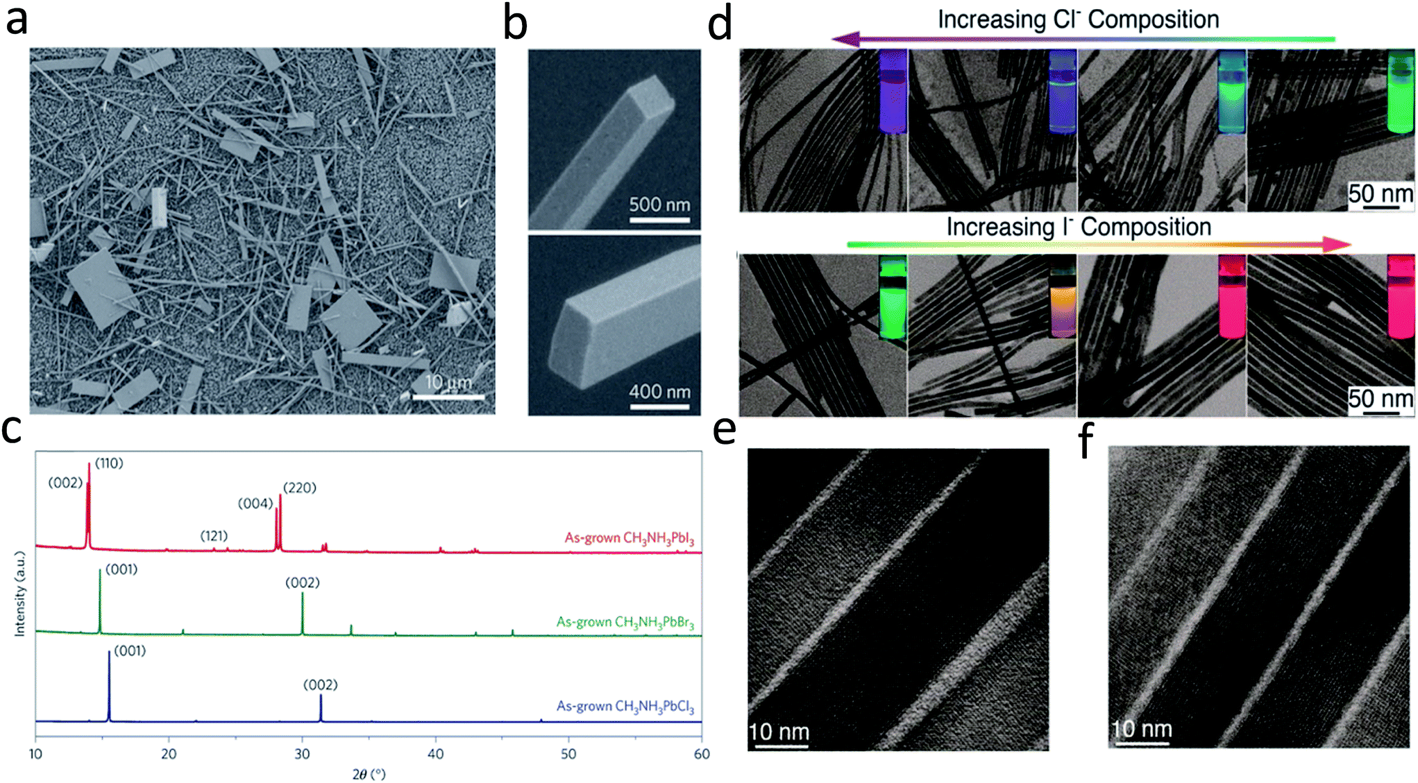 | ||
| Fig. 4 (a) and (b) SEM images of CH3NH3PbI3 nanostructures. (c) PXRD patterns of as-grown CH3NH3PbX3 (X = I, Br, Cl) NWs. (d) TEM images of CsPbX3 NWs with various degrees of conversion with chloride and iodide anions. The insets show the evolution of emission color (UV excitation, λ = 365 nm) upon forming mixed-halide CsPb(Br/Cl)3 and CsPb(Br/I)3 NWs. HRTEM images of (e) Cl- and (f) I-exchange NWs. Reprinted with permission from ref. 15 and 74, copyright 2015, Nature Publishing Group and 2016, American Chemical Society. | ||
Following this work, a solution processed method with surfactant ligand was reported to control the synthesis of all-inorganic perovskite CsPbX3 (X = Cl, Br, I or mixture of halides) nanowires.65 This method was widely used for previous metal and inorganic semiconductor nanowires, using a surfactant ligand as the capping ligand to initiate one dimensional crystal growth. The CsPbX3 nanowires were synthesized under an air-free environment by reacting cesium oleate with lead halide in the presence of oleic acid and oleylamine in octadecene at 150–250 °C for 5–10 min. Oleylamine here serves as a capping ligand of Pb2+, reducing the activity of the Pb2+ precursor. Meanwhile, oleylamine preferentially binds to certain facets of CsPbX3, leading to the anisotropic, one dimensional crystal growth to obtain perovskite nanowires. The as-synthesized CsPbX3 perovskite nanowires exhibit diameters less than 12 nm and lengths up to 5 μm. However, the production yield of the nanowires is not high and a lot of byproducts, such as nanoplatelets and nanocrystals, are produced along with the nanowires. By replacing the original oleic acid with octylamine, the nanowire yield has been dramatically improved, yielding up to 90% after simple purification.74 Moreover, by an anion exchange reaction, CsPbCl3 and CsPbI3 nanowires can be transformed from CsPbBr3 nanowires by reacting with other halide precursors, as shown in Fig. 4d and e. The nanowires transformed from CsPbBr3 nanowires exhibit a high quantum efficiency up to 83% and 30% for CsPbI3 and CsPbCl3, respectively. As shown in Fig. 4e and f, single crystalline features of CsPbI3 and CsPbCl3 are still maintained after transformations, confirmed by their HRTEM images.74 High crystallinity and excellent optical properties enable perovskite nanowires to serve as promising candidates for optoelectronic applications.
In addition to solution phase synthesis of perovskite nanowires, high quality perovskite nanowires have also been obtained through a vapor phase synthesis. Xing et al. utilized a two-step vapor phase method to synthesize high crystalline quality methylammonium lead iodide perovskite nanowires.39 Briefly, PbI2 nanowires were firstly synthesized on a silicon dioxide substrate by placing the PbI2 precursor in a chemical vapor deposition furnace. Fig. 5a shows the scanning electron microscopy image of PbI2 nanowires. PbI2 nanowires were vertically grown on the silicon dioxide substrate and possess rectangular or near square cross sections. Those nanowires were subsequently transferred to another substrate by pressing the new substrate on top of the original substrate with vertically grown nanowires, as shown in Fig. 5b. Consequently, nanowires on the new substrate were placed in the furnace for conversion into perovskites by intercalating CH3NH3I into the interval sites of PbI6 octahedra layers. The nanowire morphology was still maintained after the conversion. The converted perovskite nanowires exhibited single crystalline properties and grew along the [100] direction, which were confirmed by their SAED patterns (Fig. 5c and d). However, for this kind of two-step method, the reaction needs to be carefully controlled as an incomplete reaction will result in polycrystalline products or the dual-existence of perovskite and PbI2. With the morphology acting as an active resonator, these vapor phase grown perovskite nanowires exhibited an excellent performance in optically pumped lasing.
 | ||
| Fig. 5 (a) SEM image of PbI2 nanowires grown on the silicon substrate. (b) Optical microscopy image of CH3NH3PbI3 nanowires on the silicon substrate. Inset in (b) is the magnified image. (c) TEM and (d) HRTEM images of CH3NH3PbI3 nanowire. Inset in (c) is its corresponding SAED pattern. Reprinted with permission from ref. 39, copyright 2015, American Chemical Society. | ||
2.3 Perovskite nanoplatelets
Among all low dimensional forms, 2D materials are probably the most important one for practical applications in optoelectronic devices. Because its lateral size is at macro-scale, a 2D material can be easily integrated with other existing electronic materials in a scalable way. The stacking of different 2D materials in a designable configuration can create sophisticated devices, such as FETs, photodetectors, LEDs, and solar cells, and is usually difficult to achieve in a single crystal of 0D or 1D materials. Nanoplatelets, a quasi-form of 2D material, have a lateral size of tens of micrometers and a thickness of a few to a few tens of nanometers. In research, it is usually easier to prepare 2D materials in the form of nanoplatelets or nanoflakes rather than a millimeter scale film. The fact that the nanoplatelet is defect-free, a high quality single crystal, and has a large lateral size that is enough for any optical or electronic characterization makes it a preferred subjected for 2D material studies. The perovskite material is no exception. Our group was among the first to report the synthesis of lead halide perovskite nanoplatelets using a home-built vapor deposition system as illustrated in Fig. 6.41 In this two-step method, first lead halide crystals were grown on a muscovite mica substrate utilizing the van der Waals epitaxial growth mechanism (Fig. 6a). The super smooth surface of the freshly cleaved mica and low lattice mismatch between the lead halide lattice constants and those of the mica endure the horizontal growth of the crystals, which results in nanoplatelet formation. The as-grown lead halide nanoplatelets were then intercalated with methylammonium halide using the same vapor deposition system, which converted the nanoplatelets into respective perovskites (Fig. 6b). After conversion, the perovskite nanoplatelet thickness was increased by the factor of ∼1.8 while retaining lateral dimensions comparable to their PbI2 counterparts (Fig. 6c), which is in good agreement with the theoretical calculation based on the crystal structures of the two compounds. The resulting perovskite nanoplatelets were shown to have excellent optical properties and high crystallinity. The CH3NH3PbI3 nanoplatelet was shown to have twice the electron diffusion length of the solution processed film. | ||
| Fig. 6 Morphological characterizations of lead halide nano-platelets as-grown on a muscovite mica substrate: (a) optical (above) and SEM (below) images of lead halides: A, D: PbCl2; B, E: PbBr2; C, F: PbI2. (b) Schematic of the synthesis setup using a home-built vapor-transport system. (c) Thickness of PbI2 platelets before (images above data line) and after being converted to CH3NH3PbI3 (images below data line). Note that the color of the PbI2 platelets changes, corresponding to the change in thickness (as measured by AFM). (d) Optical properties of different lead halide perovskites (CH3NH3PbX3). Reprinted with permission from ref. 41, copyright 2014, Advance Optical Materials. | ||
Liu et al.76 introduced a different approach using a hot casting aqueous solution of PbI2 on a SiO2 substrate to form PbI2 nanoplatelets and then converted them to perovskite by intercalating methylammonium halide using a vapor deposition system. Due to the layered structure of PbI2, the crystals tend to self-assemble into platelets in its aqueous solution during the hot casting process. Thanks to their layered structure, the PbI2 nanoplatelets can also be prepared by mechanical exfoliation from the bulk crystals as reported by Cheng et al.77 The similarity between the three methods above is that they are all two-step methods in which the physical growth of lead halide nanoplatelets is followed by vapor phase intercalation of methylammonium halide. These approaches, especially the first one – using a vapor deposition system for all steps, have the advantage of using high purity sources of precursors and eliminating the possible contamination and by-product production during synthesis. However, due to the two-step growth and the solid phase intercalation of lead halide, the crystallinity of the resulting perovskite nanoplatelets may not be as good as in the single crystal growth in the solution phase.
Wang et al. reported a simple method to grow single crystal perovskite microplates.78 Perovskite in N,N-dimethylformamide (DMF) solution was drop-casted onto a hydrophobic substrate (i.e. ITO scribed with polyethylene film). The formation of self-assembled microplates was controlled by the volume ratio of perovskite solution and an anti-solvent – dichloromethane (DCM). The dispersion of DCM vapor in the perovskite solution induced the nucleation and subsequent growth of perovskite microplates. The above methods were applied to 3D-structured perovskites where the thickness of the nanoplatelets was in the order of tens or even hundreds of nanometers. The nature of the 3D crystalline structure of these perovskites makes them difficult to prepare at mono- or even few layers thick. The other type of perovskite, which has a 2D layered structure, may be a better candidate to study the 2D form. Indeed, Dou et al.34 has reported a solution method to prepare monolayer square sheets of (C4H9NH3)2PbI4 which opened up a new direction to study perovskite at an atomically thin level comparable with other 2D materials such as graphene or TMD. The result is summarized in Fig. 7.
 | ||
| Fig. 7 Synthesis of atomically thin 2D (C4H9NH3)2PbBr4 crystals. (A) Structural illustration of a single layer (C4H9NH3)2PbBr4 (blue balls, lead atoms; large orange balls, bromine atoms; red balls, nitrogen atoms; small orange balls, carbon atoms; H atoms were removed for clarity). (B) Optical image of the 2D square sheets. Scale bar, 10 mm. (C) AFM image and height profile of several single layers. The thickness is around 1.6 nm (T 0.2 nm). (D) AFM image and height profile of a double layer. The thickness is around 3.4 nm (T 0.2 nm). Reprinted from ref. 34, Copyright 2015, Science Publishing Group. | ||
In this method, a very diluted solution of perovskite in a co-solvent system of chlorobenzene (CB), acetonitrile and DMF was dropped onto a Si/SiO2 substrate prior to mild heating of the substrate to induce crystal growth of the perovskite square sheets. The co-solvent system played an important role as CB and acetonitrile help to reduce the solubility of perovskite in DMF and promote the crystallization. The diluted solution of perovskite (i.e. 10−3 M) was also critical to obtain monolayer sheets.
One of the common methods to prepare nanosheets in the literature is to use a surfactant as a morphology assisting agent during the growth of a material in solution. Despite the fact that using a surfactant will result in contamination of the surface of the grown materials and may eventually reduce their performance in electronic properties, this is one of the few methods that provide high throughput and reproducibility. Song et al.79 and Sun et al.53 both applied similar approaches to synthesize nanoplatelets of cesium lead bromide perovskite (CsPbBr3). Both methods used long-chain alkyl amines such as oleylamine, dodecylamine, octylamine, and long-chain carboxylic acids such as oleic acid as co-surfactants. Instead of using cesium halide as a precursor like the other method, they used carboxylates of cesium such as cesium oleate or cesium stearate for better solubility in the hydrocarbon solvent, which was the medium for the reaction. The result is that they can synthesize nanoplatelets on a large scale with high monodispersity and control the thickness of the perovskite down to a monolayer, as shown in Fig. 8.79
 | ||
| Fig. 8 Synthesis of 2D ultrathin CsPbBr3 nanosheets: (a) low-magnification and (b) high-magnification SEM images. AFM image and height profile of (c) monolayer and (d) bilayer CsPbBr3 nanosheets with a thickness of 1.6 and 3.3 ± 0.2 nm, respectively. (e) Thickness distribution histograms for CsPbBr3 nanosheets prepared through solution-phase synthesis. Reprinted from ref. 79, copyright 2016, Advanced Materials. | ||
3. Optical properties and applications of metal halide perovskite nanomaterials
3.1 Optical properties
 | ||
| Fig. 9 (a) Colloidal perovskite CsPbX3 NCs (X = Cl, Br, I) solutions in toluene under an UV lamp (λ = 365 nm); (b) representative PL spectra (λexc = 400 nm for all but 350 nm for CsPbCl3 nanocrystals). (c) Optical absorption and PL spectra of CsPbCl3, CsPbBr3, and CsPbI3 nanoplatelets. Inset: PL image of CsPbCl3, CsPbBr3, and CsPbI3 nanoplatelets. Reprinted with permission from ref. 40 and 49, copyright 2015, American Chemical Society and 2016, Advanced Material. | ||
 | ||
| Fig. 10 (a) Quantum-size effects in the absorption and emission spectra of 5–12 nm CsPbBr3 NCs. (b) Experimental versus theoretical (effective mass approximation, EMA) size dependence of the band gap energy. Reprinted with permission from ref. 49. | ||
3.2 Applications in optoelectronics
 | ||
| Fig. 11 Optical lasing in lead halide perovskite nanoplatelets and nanowires. (a) Whisper-gallery mode lasing in a perovskite nanoplatelet cavity. (b) Fabry-Pérot lasing in a perovskite nanowire cavity. (c) Photoluminescence spectra of CsPbX3 (X = Cl, Br, I) nanoplatelets. (d) Wavelength tunability of perovskite lasing by changing the content of halide in CsPbX3 perovskite. Reprinted with permission from ref. 14, 15 and 40. | ||
Zhu et al. demonstrated lasing in CH3NH3PbX3 with an exceptionally low threshold of only 220 nJ cm−2 (Fig. 11b), corresponding to a carrier density as low as 1.5 × 1016 cm−3. Another remarkable thing about the nanowires is that they have a very low number of carrier trapping sites and the estimated lasing quantum yield is close to 100%.15 We believe that in addition to high optical gain, the high quality crystalline structure of these perovskite nanowires and nanoplatelets is responsible for their high performance as a self-lasing material. With their exceptional coherent light emission and their ambipolar charge transport properties, the perovskite materials may someday be applied in electrically driven lasing.
 | ||
| Fig. 12 Low dimensional perovskite in LED applications. (a) LED from CH3NH3PbX3 quantum dots. (b) LED from CsPbX3 quantum dots. (c) LED from CH3NH3PbX3 nanoplatelets. Reprinted with permission from ref. 17, 90 and 91. | ||
4. Conclusions and outlook
Metal halide perovskites represent a vast family of interesting semiconducting materials with exceptional optical and electronic properties. Unlike traditional III–V or II–VI semiconductors, there are thousands of combinations of perovskite compositions that can be easily synthesized. This provides a facile method to tune the characteristics of the material, such as the band-gap, conductivity, mobility, and so forth, which are very important for device configuration and optimization. The abundance of the material, low cost, and high performance of perovskite make this a promising material for future optoelectronic applications.However, one of the biggest problems for this type of material is its stability. Due to the vulnerability of perovskite to surrounding environments such as moisture and oxygen, the performance of the devices may dramatically drop within only tens to hundreds of exposed hours, which casts a shadow towards their practical applications. Perovskite nanomaterials with high surface areas may seriously suffer from the effects of the environment. Thus, the need to develop a method to stabilize the material is inevitable either by chemical approaches such as capping agents, stabilizers or by physical approaches such as device encapsulation. It is well-known that 2D structured perovskites are normally more stable than their 3D counterparts. This is because the long chain organic cations in the 2D perovskite act like a protecting layer insulating MX6 octahedral structures from environmental agents (i.e. moisture, oxygen). However, these organic layers also hinder the charge transport in 2D perovskite resulting in their poor performance in optoelectronic applications compared to the 3D counterparts. If the conductivity of 2D structured perovskite can be improved, one can expect a high performance, stable perovskite device. Indeed, in a recent report in Nature, Tsai et al. demonstrated the use of a 2D–3D hybrid structural perovskite in a high performance and long-time stable solar cell device.12 By changing the composition of CH3NH3+ (3D component) and C4H9NH3+ (2D component) in the lead iodide perovskite formula, they were able to tune the crystal planes parallel to the substrate surface from 001 (in 2D perovskite) to 101 (in 2D–3D hybrid perovskite). Thus, the PbI6 octahedra network will come into direct contact with both the anode and cathode of the cell to facilitate efficient charge transport. The resulting cell exhibits an efficiency of 12.52% with no hysteresis and retained over 90% of its original efficiency after 3000 hours. This is a milestone in perovskite research, which is an ultimate solution to the biggest problem of the material. We can expect to see many efforts to synthesize perovskite nanomaterials with this hybrid formula and their applications in optoelectronics in the future.
There is still room for chemists to improve the optical and electronic properties of perovskite by tailoring the chemistry and crystallographic sciences. The next generation of this material may be truly multifunctional organic hybrid perovskites with application-driven compound design. We need to understand thoroughly the functions of each component in the perovskite formula such as organic cations, metal halide octahedra network and the effect of each on the entire crystal structure in order to formulate a better compound for different applications. This is an unusual but fantastic class of semiconductors where every characteristic (i.e. band structure, conductivity, mobility etc.) can be finely tuned to suit any requirement of a material. The future of the material is very much dependent on chemical scientists further exploring the thousands of unknown combinations of the perovskite out there.
Acknowledgements
Q. H. Xiong gratefully acknowledges the strong support for this work from the Singapore National Research Foundation through an Investigatorship Award (NRF-NRFI2015-03) and a Competitive Research Program (NRF-CRP-6-2010-2), and Singapore Ministry of Education via two AcRF Tier 2 grants (MOE2013-T2-1-049 and MOE2015-T2-1-047), Tier 1 grant (2013-T1-002-232). Q. Zhang would like to thank the Peking University and China National Young Thousand Talents Program for start-up funding support.References
- K. S. Novoselov, et al. , Science, 2004, 306, 666 CrossRef CAS PubMed.
- L. Song, et al. , Nano Lett., 2010, 10, 3209 CrossRef CAS PubMed.
- M. P. Levendorf, et al. , Nature, 2012, 488, 627 CrossRef CAS PubMed.
- S. Najmaei, et al. , Nat. Mater., 2013, 12, 754 CrossRef CAS PubMed.
- M. Chhowalla and G. A. Amaratunga, Nature, 2000, 407, 164 CrossRef CAS PubMed.
- J. Feng, et al. , Nature, 2016, 536, 197 CrossRef CAS PubMed.
- W. Wu, et al. , Nature, 2014, 514, 470 CrossRef CAS PubMed.
- L. K. Li, et al. , Nat. Nanotechnol., 2014, 9, 372 CrossRef CAS PubMed.
- E. S. Reich, Nature, 2014, 506, 19 CrossRef PubMed.
- J. Burschka, et al. , Nature, 2013, 499, 316 CrossRef CAS PubMed.
- M. Liu, M. B. Johnston and H. J. Snaith, Nature, 2013, 501, 395 CrossRef CAS PubMed.
- H. Tsai, et al. , Nature, 2016, 536, 312 CrossRef CAS PubMed.
- G. Xing, et al. , Nat. Mater., 2014, 13, 476 CrossRef CAS PubMed.
- Q. Zhang, S. T. Ha, X. Liu, T. C. Sum and Q. Xiong, Nano Lett., 2014, 14, 5995 CrossRef CAS PubMed.
- H. Zhu, et al. , Nat. Mater., 2015, 14, 636 CrossRef CAS PubMed.
- Z. K. Tan, et al. , Nat. Nanotechnol., 2014, 9, 687 CrossRef CAS PubMed.
- J. Xing, et al. , ACS Nano, 2016, 10, 6623 CrossRef CAS PubMed.
- M. Yuan, et al. , Nat. Nanotechnol., 2016, 11, 872 CrossRef CAS PubMed.
- Gurudayal, et al. , Nano Lett., 2015, 15, 3833 CrossRef CAS PubMed.
- J. Luo, et al. , Science, 2014, 345, 1593 CrossRef CAS PubMed.
- S. T. Ha, C. Shen, J. Zhang and Q. H. Xiong, Nat. Photonics, 2016, 10, 115 CrossRef CAS.
- E. Yablonovitch, Science, 2016, 351, 1401 CrossRef CAS PubMed.
- A. Kojima, K. Teshima, Y. Shirai and T. Miyasaka, J. Am. Chem. Soc., 2009, 131, 6050 CrossRef CAS PubMed.
- H. S. Kim, et al. , Sci. Rep., 2012, 2, 591 Search PubMed.
- X. Li, et al. , Science, 2016, 353, 58 CrossRef CAS PubMed.
- D. Shi, et al. , Science, 2015, 347, 519 CrossRef CAS PubMed.
- S. D. Stranks, et al. , Science, 2013, 342, 341 CrossRef CAS PubMed.
- G. C. Xing, et al. , Science, 2013, 342, 344 CrossRef CAS PubMed.
- D. B. Mitzi, C. A. Feild, W. T. A. Harrison and A. M. Guloy, Nature, 1994, 369, 467 CrossRef CAS.
- K. Chondroudis and D. B. Mitzi, Chem. Mater., 1999, 11, 3028 CrossRef CAS.
- D. B. Mitzi, C. A. Feild, Z. Schlesinger and R. B. Laibowitz, J. Solid State Chem., 1995, 114, 159 CrossRef CAS.
- D. B. Mitzi, et al., Abstr. Pap. Am. Chem. Soc., 2002, 223, C23 Search PubMed.
- A. Lemmerer, PhD thesis, University of the Witwatersrand, Johannesburg, 2007.
- L. T. Dou, et al. , Science, 2015, 349, 1518 CrossRef CAS PubMed.
- H. Deng, et al. , Nanoscale, 2015, 7, 4163 RSC.
- J. H. Im, et al. , Nano Lett., 2015, 15, 2120 CrossRef CAS PubMed.
- Y. S. Park, S. J. Guo, N. S. Makarov and V. I. Klimov, ACS Nano, 2015, 9, 10386 CrossRef CAS PubMed.
- J. A. Sichert, et al. , Nano Lett., 2015, 15, 6521 CrossRef CAS PubMed.
- J. Xing, et al. , Nano Lett., 2015, 15, 4571 CrossRef CAS PubMed.
- Q. Zhang, et al. , Adv. Funct. Mater., 2016, 26, 6238 CrossRef CAS.
- S. T. Ha, et al. , Adv. Opt. Mater., 2014, 2, 838 CrossRef CAS.
- X. Zhang, et al. , Nano Lett., 2016, 16, 1415 CrossRef CAS PubMed.
- L. C. Schmidt, et al. , J. Am. Chem. Soc., 2014, 136, 850 CrossRef CAS PubMed.
- S. Gonzalez-Carrero, R. E. Galian and J. Perez-Prieto, J. Mater. Chem. A, 2015, 3, 9187 CAS.
- F. Zhang, et al. , ACS Nano, 2015, 9, 4533 CrossRef CAS PubMed.
- H. Huang, A. S. Susha, S. V. Kershaw, T. F. Hung and A. L. Rogach, Adv. Sci., 2015, 2, 1500194 CrossRef PubMed.
- D. H. Cao, C. C. Stoumpos, O. K. Farha, J. T. Hupp and M. G. Kanatzidis, J. Am. Chem. Soc., 2015, 137, 7843 CrossRef CAS PubMed.
- L. N. Quan, et al. , J. Am. Chem. Soc., 2016, 138, 2649 CrossRef CAS PubMed.
- L. Protesescu, et al. , Nano Lett., 2015, 15, 3692 CrossRef CAS PubMed.
- (a) G. Nedelcu, et al. , Nano Lett., 2015, 15, 5635 CrossRef CAS PubMed; (b) Q. A. Akkerman, V. D’Innocenzo, S. Accornero, A Scarpellini, A. Petrozza, M. Prato and L. Manna, J. Am. Chem. Soc., 2015, 137, 10276 CrossRef CAS PubMed.
- A. Swarnkar, et al. , Angew. Chem., Int. Ed., 2015, 54, 15424 CrossRef CAS PubMed.
- X. M. Li, et al. , Adv. Funct. Mater., 2016, 26, 2435 CrossRef CAS.
- S. B. Sun, D. Yuan, Y. Xu, A. F. Wang and Z. T. Deng, ACS Nano, 2016, 10, 3648 CrossRef CAS PubMed.
- J. De Roo, et al. , ACS Nano, 2016, 10, 2071 CrossRef CAS PubMed.
- A. Swarnkar, et al. , Science, 2016, 354, 92 CrossRef CAS PubMed.
- L. Dou, et al. , Nat. Commun., 2014, 5, 5404 CrossRef CAS PubMed.
- F. Deschler, et al. , J. Phys. Chem. Lett., 2014, 5, 1421 CrossRef CAS PubMed.
- A. Brehier, R. Parashkov, J. S. Lauret and E. Deleporte, Appl. Phys. Lett., 2006, 89, 171110 CrossRef.
- X. Hu, et al. , Adv. Funct. Mater., 2014, 24, 7373 CrossRef CAS.
- Y. Lee, et al. , Adv. Mater., 2015, 27, 41 CrossRef CAS PubMed.
- H. Zhou, et al. , Science, 2014, 345, 542 CrossRef CAS PubMed.
- S. W. Eaton, et al. , Proc. Natl. Acad. Sci. U. S. A., 2016, 113, 1993 CrossRef CAS PubMed.
- Y. Fu, et al. , ACS Nano, 2016, 10, 7963 CrossRef CAS PubMed.
- Y. P. Fu, et al. , Nano Lett., 2016, 16, 1000 CrossRef CAS PubMed.
- D. D. Zhang, S. W. Eaton, Y. Yu, L. T. Dou and P. D. Yang, J. Am. Chem. Soc., 2015, 137, 9230 CrossRef CAS PubMed.
- M. H. Huang, et al. , Science, 2001, 292, 1897 CrossRef CAS PubMed.
- U. Özgür, et al. , J. Appl. Phys., 2005, 98, 041301 CrossRef.
- R. Chen, et al. , Nano Lett., 2010, 10, 4956 CrossRef CAS PubMed.
- F. Vietmeyer, P. A. Frantsuzov, B. Janko and M. Kuno, Phys. Rev. B: Condens. Matter Mater. Phys., 2011, 83, 115319 CrossRef.
- X. Xu, et al. , ACS Nano, 2011, 5, 3660 CrossRef CAS PubMed.
- W. S. Yang, et al. , Science, 2015, 348, 1234 CrossRef CAS PubMed.
- W. Nie, et al. , Science, 2015, 347, 522 CrossRef CAS PubMed.
- S. Yakunin, et al. , Nat. Commun., 2015, 6, 8056 CrossRef CAS PubMed.
- D. Zhang, et al. , J. Am. Chem. Soc., 2016, 138, 7236 CrossRef CAS PubMed.
- Y. Fu, et al. , J. Am. Chem. Soc., 2015, 137, 5810 CrossRef CAS PubMed.
- J. Y. Liu, et al. , ACS Nano, 2016, 10, 3536 CrossRef CAS PubMed.
- H. C. Cheng, et al. , Nano Lett., 2016, 16, 367 CrossRef CAS PubMed.
- K. Y. Wang, et al. , ACS Photonics, 2016, 3, 1125 CrossRef CAS.
- J. Z. Song, et al. , Adv. Mater., 2016, 28, 4861 CrossRef CAS PubMed.
- J. Wang, et al. , Adv. Mater., 2015, 27, 2311 CrossRef CAS PubMed.
- W. L. Hong, et al. , Adv. Mater., 2016, 28, 8029 CrossRef CAS PubMed.
- S. G. R. Bade, et al. , ACS Nano, 2015, 10, 1795 CrossRef PubMed.
- G. Li, et al. , Adv. Mater., 2016, 28, 3528 CrossRef CAS PubMed.
- S. A. Veldhuis, et al. , Adv. Mater., 2016, 28, 6804 CrossRef CAS PubMed.
- D. Liang, et al. , ACS Nano, 2016, 10, 6897 CrossRef CAS PubMed.
- N. Yantara, et al. , J. Phys. Chem. Lett., 2015, 6, 4360 CrossRef CAS PubMed.
- F. Zhang, et al. , ACS Nano, 2015, 9, 4533 CrossRef CAS PubMed.
- Y. Fu, et al. , Nano Lett., 2016, 16, 1000 CrossRef CAS PubMed.
- K. Wu, et al. , J. Am. Chem. Soc., 2015, 137, 12792 CrossRef CAS PubMed.
- J. Z. Song, et al. , Adv. Mater., 2015, 27, 7162 CrossRef CAS PubMed.
- Y. C. Ling, et al. , Adv. Mater., 2016, 28, 305 CrossRef CAS PubMed.
| This journal is © The Royal Society of Chemistry 2017 |