 Open Access Article
Effect of electrical injection-induced stress on interband transitions in high Al content AlGaN MQWs
Jinjian Zhenga,
Jinchai Li *a,
Zhibai Zhonga,
Wei Lina,
Li Chena,
Kongyi Lia,
Xinghe Wangb,
Chilun Choub,
Shuiqing Lib and
Junyong Kang*a
aDepartment of Physics, Fujian Provincial Key Laboratory of Semiconductor Materials and Applications, Xiamen University, Xiamen, 361005, P. R. China. E-mail: jinchaili@xmu.edu.cn; jykang@xmu.edu.cn; Fax: +86-592-2187737; Tel: +86-592-2185962
bSan'an Optoelectronics Co., Ltd., Xiamen, 361005, P. R. China
First published on 5th December 2017
Abstract
The light extraction from AlGaN deep ultraviolet light-emitting diodes (UV LEDs) is known to be limited by the fundamental valence band crossover issue. To study the effect of electrical injection on the complex structure of the valence bands, stress variations were characterized by the Raman shift of AlGaN deep UV LEDs under electrical injection. Results show that tensile stress builds up as the current increases. The first-principles simulations reveal that, as the tensile strain increases, the crystal-splitting hole band becomes more dominant at the top of valence bands and exhibits stronger dispersion along the Γ–A direction, leading to stronger TM polarized emission and a decrease of the total spontaneous emission rate. Furthermore, a promising way of controlling AlGaN MQWs under strain-free or compressive strain status is proposed to improve the transverse electric polarized emission and quantum efficiency in deep UV LEDs.
1. Introduction
AlGaN-based deep ultraviolet (UV) light-emitting diodes (LEDs) are attracting much interest for their promising applications in water purification, data storage, medical treatment, bio-chemical agent detection, and photolithography.1–3 However, despite the tremendous progress in terms of defect density, carrier confinement and p-type doping, low external quantum efficiency is still an obstacle to wide use. One major limitation to the external quantum efficiency is the poor light extraction efficiency arising from the fundamental valence band crossover issue.4,5 For high Al-content AlGaN multiple quantum wells (MQWs), the crystal field split-off hole (CH) band is on the top of the valence band, resulting in dominant transverse-magnetic (TM) polarized emission, i.e., the electric field vector is parallel to the (0001) c-axis (E∥c).6–9 TM (E∥c) polarized emission will propagate perpendicularly to the c-axis and will not easily escape from the light escape cone,10 which inherently increases with increasing Al content,11 resulting in poor light extraction efficiency for deep UV LEDs. Moreover, except for the high Al content, several studies have reported that the transverse electric (TE, E⊥c) polarization switches to TM (E∥c) polarization at high current injection, making the efficiency drop become more serious.6–8 It is known that the strength and fraction of the two (TE and TM) polarized emissions from AlGaN MQWs are determined by the interband transitions between conduction bands and valence bands. Although the influence of carrier density on polarization switching is theoretically interpreted as resulting from the occupation of the higher states above k = 0 with increasing the injection current,7,8 the effect of electrical injection on the complex structure of the valence bands remains controversial.Traditionally, the injected electrons should be much larger than the injected holes in the III-nitride based LED due to the difficulty of p-type doping, leading to the electron accumulation in the active region. In previous study, a tensile stress induced by the electron accumulation has been demonstrated in the active region of GaN-based blue LEDs under electrical injection, which results in the reduction of the transition probability among quantum levels so as to the efficiency droop.12 The problem of electron accumulation should be more severe in deep UV LEDs because that the p-type doping efficiency is known to be extremely low in high-Al content AlGaN. In this work, the effect of electrical injection-induced stress on interband transition as well as the optical polarization in high Al content AlGaN MQWs was comprehensively studied. The stress variations were characterized by the Raman shift of AlGaN deep UV LEDs under electrical injection. Strain dependent electronic structures of AlGaN MQWs were investigated by the first-principles calculations. The results demonstrated that a tensile strain was induced by the electrical injection, leading the CH band became more dominant at the top of valence bands and exhibited stronger dispersion along the Γ–A direction. Thus, the proportion of TM polarized emission increases with increasing the injection-current. In addition, it is promising to control AlGaN MQWs under strain-free or compressive strain status to improve the TE polarized emission and quantum efficiency in deep UV LEDs.
2. Experiments and calculations
One AlGaN deep UV LED structure and four AlxGa1−xN films with Al content of 0.3, 0.5, 0.7 and 0.9, respectively, were grown on c-plane (0001) sapphire substrates via metal organic chemical vapor deposition. The LED structure consisted of an AlN buffer layer, a 2 μm-thick n-type Al0.55Ga0.45N layer, a five pairs of Al0.45Ga0.55N (5 nm)/Al0.55Ga0.45N (15 nm) MQWs layer with Si-doped barriers, an electron blocking layer (EBL), and a p-GaN contact layer, as shown in Fig. 1(a). The average Al content and the period thickness of MQWs were about 0.52 and 20 nm, respectively, determined by the secondary ion mass spectroscopy. The LEDs were flip-chip mounted and the electroluminescence emitted from the sapphire substrate. 2 μm-thick AlxGa1−xN bulk layers with different Al content were grown on AlN buffer layers deposited on c-plane (0001) sapphire substrates, as illustrated in Fig. 1(b). The contents were ascertained by X-ray diffraction. Raman scattering measurements were performed under different injection current by using a Raman microscope (Renishaw UV-vis 1000) with a 532 nm laser. The spectra from 100 cm−1 to 1000 cm−1 were collected through backscattering configuration with an incident light perpendicular to the sample surface. To eliminate the self-heating effect, the UV LED was packaged with a heat spreading layer and operated under pulsed current mode with a pulse frequency of 1 kHz and duty of 0.1%.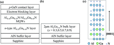 | ||
| Fig. 1 Schematics of (a) the LED structure and (b) AlGaN films grown by MOVPE, (c) crystal structure of (Al0.50Ga0.50N)2/(AlN)6 MQWs. | ||
The first-principles calculations were carried out using the Vienna Ab initio Simulation Package (VASP) employing the pseudopotentials specified using the projector augmented wave (PAW) method. A geometric structure of (Al0.50Ga0.50N)2/(AlN)6 MQWs was modeled by 2 × 2 × 4 periodic supercell to simplify the calculation and approach to the grown structures, as shown in Fig. 1(c). The well layer was composed of 2 × 2 × 1 unit cells of Al0.50Ga0.50N, in which the Al atoms are evenly distributed, and the barrier was constructed by 2 × 2 × 3 unit cells of AlN. The volume and shape of the supercell, and the internal positions of the atoms were initially defined by the AlN and GaN parameters, which were close to the practical epitaxial growth systems and allowed to be simultaneously relaxed to the equilibrium. The Davidson-block iteration scheme was applied to optimize the energy of the electronic state until the stopping criterion of 0.1 meV was fulfilled. Structural optimization was carried out by relaxing all degrees of freedom using the conjugate gradient algorithm and the total energy is converged within 1 meV for all the systems. A plane-wave basis set with 500 eV cutoff was used to expand the electronic wave functions at special k points generated by a 8 × 8 × 8 Monkhurst-Pack scheme. The Ga 3d electrons were treated as core electrons. The additional neutralizing background charge was applied by means of the VASP simulations.
3. Results and discussions
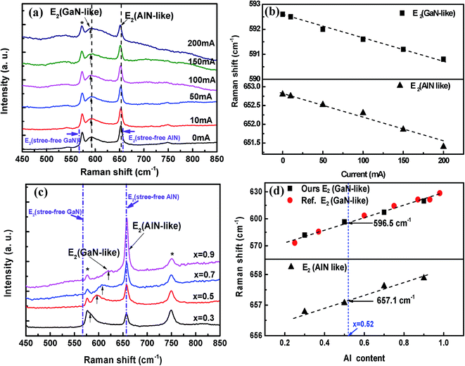
Generally, MQWs suffers the biggest voltage drop under the current injection, which might generate the variation of junction temperature and stress. In this work, the self-heating effect has been eliminated by operating the deep UV LED under pulsed current mode. Thus, the effect of stress variation becomes the focus, which is known to have great influence on the optical polarization of the deep UV LEDs.13 A direct measurement via Raman microscope developed in previous work was carried out when the deep UV LEDs driving at different currents.12 As shown in Fig. 2(a) and (b), the Raman spectra of deep UV LEDs display the typical E2 (GaN-like) mode at 592.6 cm−1 and the E2 (AlN-like) mode at 652.8 cm−1 allowed by Raman selection rule before current injection.14–16 The asterisks (*) denote sapphire substrate signal. The significant upshift of 64.5 cm−1 in the E2 (GaN-like) mode with respect to that of stress-free GaN16 (567 cm−1) can mainly be attributed to the high Al content containing in the LED structure, which will be discussed later. When the injection current increases, the E2 (GaN-like) and E2 (AlN-like) modes decrease monotonically and reaches 590.8 cm−1 and 651.4 cm−1 with a downshift of 1.8 and 1.4 cm−1, respectively, when the driving current increases to 200 mA. This current dependent trend of Raman shift is essentially in agreement with our previous results of GaN based LEDs.12 As has been reported, the E2 (GaN-like) mode is sensitive to strain or composition in AlGaN layer.14–16 A downshift in the E2 mode is observed as a result of relaxation of compressive strain, increase of tensile strain, or decrease of Al content. Obviously, the Raman frequency decrease with the current injection is attributed to the strain variation. On account of the deep UV LED structure, the Raman shift may originate from n-AlGaN layer, MQWs, and EBL, in which containing high Al content. Nevertheless, the MQWs layer as a recombination center in LED will induce large charge density causing the most voltage drops. Considering the almost linear feature of Raman shift, we deduced that, among other layer containing AlGaN, the MQWs layer implicitly has a more sensitive Raman response accountable for the peak shift.12 Therefore, relaxation of compressive strain or increase of tensile strain is expected to occur in the MQWs layer as injection current increases. Since it is hardly to distinguish the strain variation from quantum well and barrier layers, the average influence in MQWs with the average Al content of 0.52 will be discussed later.Given that the E2 phonon frequency is affected by the biaxial stress, the E2 (GaN-like) and E2 (AlN-like) phonon frequency shifts Δω can be used to characterize the biaxial stress σa of the AlGaN layer according to the following relationship:17
 | (1) |
Based on the above relation, the biaxial stress in the active region under different injection currents can be determined through the E2 (GaN-like) and E2 (AlN-like) phonon frequency shifts Δω with respect to that in unstressed AlGaN, in which the average Al content of MQWs (0.52) is used. Therefore, it is necessary to know the phonon frequency of AlGaN with Al content similar to that in MQWs layer. Then AlxGa1−xN films (∼2 μm) with different Al content AlxGa1−xN (x = 0.3, 0.5, 0.7, 0.9) were grown and characterized by Raman scattering. Raman spectra of AlxGa1−xN bulk layers with different Al content x are plotted in Fig. 2(c). The E2 (GaN-like) and E2 (AlN-like) modes are located at about 582 cm−1 and 656.8 cm−1 for the sample with x = 0.3, respectively, which shift to higher frequency with increasing x to 0.9. The E2 phonon frequencies affected by the Al content x are shown in Fig. 2(d). It is interesting to observe that the E2 (GaN-like) phonon frequency ω increases significantly and almost linearly with the Al content at an intermediate range from 0.3 to 0.9, which coincident with previously reported data of Al-content-dependent Raman shift,14,16 as shown by the red-circle points in Fig. 2(d). While the E2 (AlN-like) phonon frequency increases slightly. These phenomena indicate that E2 (GaN-like) phonon frequency is much more sensitively affected by the Al content. And it is worth to note that the E2 (AlN-like) phonon frequency in the Al0.5Ga0.5N films is very close to that of stress-free AlN film16 (657 cm−1), suggesting the AlGaN films we grown are almost stress free. Consequently, the E2 (GaN-like) phonon frequency of unstressed Al0.52Ga0.48N was evaluated to locate at 596.5 cm−1 according to the tendency of E2 (GaN-like) mode.
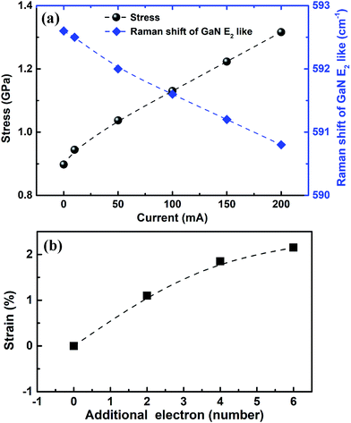
Then the injection-current dependence of stress variation in the active region is evaluated according to eqn (1), in which the current-dependent Raman shift of E2 (GaN-like) modes were compared to that of unstressed Al0.52Ga0.48N (596.5 cm−1). As can be seen from Fig. 3(a), before current injection, the active layer suffers tensile stress of 0.90 GPa. As the current increases, the E2 (GaN-like) phonon frequency shift to lower frequency, and the tensile stress increases monotonically. The tensile stress increases by 0.42 GPa when the driving current increases to 200 mA. As discussed above, much severe electron accumulation is expected in the AlGaN based LEDs. To understand such lattice structures variation in AlGaN based MQWs, the first-principles calculations were carried out under different additional numbers of electrons. By introducing additional neutralizing background charge, the lattice constants of the a-axis and c-axis are found to become larger with respect to that of equilibrium values. And they increase as the number of additional electrons rises, suggesting the tensile strain builds up as the additional number of electrons accumulate.12 Fig. 3(b) illustrates the strain variation deduced from the change of lattice constants as a function of the additional number of electrons. The tensile strain almost increases linearly with electrons accumulate and is about 2.15% while the additional number of electrons increases to 6. This tendency is consisting of the results obtained in Raman spectra, demonstrating that a tensile strain has been induced by the electrical injection.
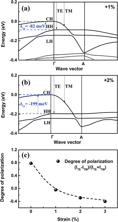
It is well known that the strain influences the electronic structures of III-nitrides.18,19 The electronic structures of AlGaN MQWs under different strains were further analyzed. Biaxial strain range from −2% to +3% were considered here. A certain value of the biaxial strain was applied by changing the in-plane lattice parameter equally, and crystal structure was allowed to relax along the out-off-plane direction.18 Fig. 4(a) and (b) illustrate the valence band structures of the Al0.50Ga0.50N/AlN MQWs with a +1% and a +2% tensile strain, respectively. When the MQWs experiences a +1% tensile strain, the CH band is lifted upward by 105 meV with respect to that of unstrained state, resulting in a negative value of crystal-field splitting energy (Δcr = −82 meV). Moreover, in contrast to the discrete quantum states in QWs, the CH band exhibits strong energy dispersion and generates two band crossing and anti-crossing points among the CH, HH and LH bands along the Γ–A ([0001]) direction. These features are agree with the simulated results reported in literature.20 As the tensile strain increases to +2%, the Δcr further decreases to −199 meV, and the dispersion of CH become stronger. These unconventional features indicate that the CH bands become more dominant at the top of valence bands, and less holes are confined in the QWs as the tensile strain increases.
In general, the emission from MQWs is closely related to the transition between electron and hole levels. The transition probability is proportional to the momentum matrix element (MME). The degree of the in-plane polarization as a function of strain were calculated from the MME of HH, LH and CH bands restricted to Γ to A of the Brillouin zone,12,19–21 as shown in Fig. 4(c). The integrated intensities of TE and TM polarized MME are denoted by ITE and ITM, respectively. In the unstrained case, the degree of polarization P = (ITE − ITM)/(ITE + ITM) is positive (0.783), suggesting strong TE polarized. But, as the MQWs suffer from a +1% tensile strain, it becomes negative (−0.042), indicating the emission is dominated by TM mode. And it decreases linearly with increasing the tensile strain, meaning the increase of proportion of TM polarized out-of-plane light.22 This agrees well with the experimental results mentioned above. Consequently, it can be inferred that the increase of proportion of TM polarized emission is mainly attributed to the electrical injection-induced tensile stress in MQWs active region, which severely limit light extraction efficiency of deep UV LEDs.
Furthermore, it is interesting to find that the valence band order from top is rearranged as HH, LH, and CH, and the crystal-field splitting energy changes to positive (Δcr = 73 meV), when the tensile strain is relaxed, as illustrated in Fig. 5(a). Meanwhile, the crystal-field splitting energy is further increased by 121 meV as the MQWs experiences a −1% compressive strain. More importantly, the HH and LH bands display a feature of discrete quantum levels along the high symmetry lines from Γ to A in the Brillouin zone, as shown in Fig. 5(b), indicating hole-states are strongly localized in the QWs.20 Therefore, a dominate TE (E⊥c) polarized emission and high emission efficiency can be expected when a compressive stress is generated in the high Al-content MQWs active region.6,9,23,24 Fundamentally, the light emission efficiency is determined by the states of the top of valence bands. The total spontaneous emission rate Rsp is given by
 | (2) |
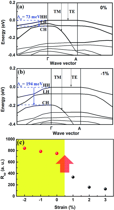 | ||
| Fig. 5 The calculated band structure under (a) unstressed state and (b) −1% compressive strain. (c) The calculated total spontaneous emission rate Rsp as a function of strain. | ||
4. Conclusions
In summary, the effect of electrical injection-induced stress on interband transition as well as the optical polarization in high Al content AlGaN MQWs have been studied. Characterized by the current-dependent Raman measurements, the Raman peaks of the E2 (GaN-like) and E2 (AlN-like) are found to gradually shift toward lower frequencies as the driving current increases, indicating a tensile stress builds up. The first-principles calculations demonstrate that electron accumulation is responsible for the stress variation. Further close inspection of strain dependent electronic structures of high Al-content MQWs reveal that, as the tensile strain increases, the CH band become more dominant at the top of valence bands and exhibits stronger dispersion along the Γ–A ([0001]) direction, leading to deconfinement of hole states and decrease of the degree of polarization. Consequently, it can be inferred that the increase of proportion of TM polarized emission is mainly attributed to the electrical injection-induced tensile stress in MQWs active region. Furthermore, as the MQWs relax to unstressed state or suffer from a compressive strain, the top of valence band recovers to be discrete quantum states for heavy holes and light holes, and the total spontaneous emission rate Rsp increases dramatically. These results suggest that controlling the strain status of high Al-content AlGaN MQWs would be a promising way to improve the TE polarized emission as well as quantum efficiency in deep UV optoelectronic devices.Conflicts of interest
There are no conflicts to declare.Acknowledgements
This work was supported by National Key R&D Program of China (2016YFB0400101), National Natural Science Foundation of China (U1405253), and the Fundamental Research Funds for the Central Universities (20720160121, 20720170012).References
- K. Balakrishnan, T. Katona and A. Khan, Nat. Photonics, 2008, 2, 77–84 CrossRef.
- Y. Taniyasu, M. Kasu and T. Makimoto, Nature, 2006, 441, 325–328 CrossRef CAS PubMed.
- J. Simon, V. Protasenko, C. Lian, H. Xing and D. Jena, Science, 2010, 327, 60–64 CrossRef CAS PubMed.
- J. W. Lee, D. Y. Kim, J. H. Park, E. F. Schubert, J. Kim, J. Lee, Y.-I. Kim, Y. Park and J. K. Kim, Sci. Rep., 2016, 6, 22537 CrossRef CAS PubMed.
- D. Y. Kim, J. H. Park, J. W. Lee, S. Hwang, S. J. Oh, J. Kim, C. Sone, E. F. Schubert and J. K. Kim, Light: Sci. Appl., 2015, 4, e263 CrossRef CAS.
- T. Kolbe, A. Knauer, C. Chua, Z. Yang, V. Kueller, S. Einfeldt, P. Vogt, N. M. Johnson, M. Weyers and M. Kneissl, Appl. Phys. Lett., 2011, 99, 261105 CrossRef.
- S.-H. Park and J.-I. Shim, Appl. Phys. Lett., 2013, 102, 221109 CrossRef.
- M. Hou, Z. Qin, C. He, J. Cai, X. Wang and B. Shen, Opt. Express, 2014, 22, 19589–19594 CrossRef PubMed.
- K. B. Nam, J. Li, M. L. Nakarmi, J. Y. Lin and H. X. Jiang, Appl. Phys. Lett., 2004, 84, 5264–5266 CrossRef CAS.
- T. Kolbe, A. Knauer, C. Chua, Z. Yang, S. Einfeldt, P. Vogt, N. M. Johnson, M. Weyers and M. Kneissl, Appl. Phys. Lett., 2010, 97, 171105 CrossRef.
- C. Netzel, A. Knauer and M. Weyers, Appl. Phys. Lett., 2012, 101, 242102 CrossRef.
- J. Zheng, S. Li, C. Chou, W. Lin, F. Xun, F. Guo, T. Zheng, S. Li and J. Kang, Sci. Rep., 2015, 5, 17227 CrossRef CAS PubMed.
- J. E. Northrup, C. L. Chua, Z. Yang, T. Wunderer, M. Kneissl, N. M. Johnson and T. Kolbe, Appl. Phys. Lett., 2012, 100, 21101 CrossRef.
- J. G. Kim, A. Kimura, Y. Kamei, N. Hasuike, H. Harima, K. Kisoda, Y. Simahara, H. Miyake and K. Hiramatsu, J. Appl. Phys., 2011, 110, 33511 CrossRef.
- C. Kisielowski, J. Krüger, S. Ruvimov, T. Suski, J. W. Ager, E. Jones, Z. Liliental-Weber, M. Rubin, E. R. Weber, M. D. Bremser and R. F. Davis, Phys. Rev. B: Condens. Matter Mater. Phys., 1996, 54, 17745–17753 CrossRef CAS.
- M. Kuball, Surf. Interface Anal., 2001, 31, 987–999 CrossRef CAS.
- L. Zhang, J. Yu, X. Hao, Y. Wu, Y. Dai, Y. Shao, H. Zhang and Y. Tian, Sci. Rep., 2014, 4, 4179 CrossRef PubMed.
- C. E. Dreyer, A. Janotti and C. G. Van De Walle, Appl. Phys. Lett., 2013, 102, 142105 CrossRef.
- S. L. Chuang and C. S. Chang, Phys. Rev. B: Condens. Matter Mater. Phys., 1996, 54, 2491–2504 CrossRef CAS.
- L. Chen, J. Zheng, W. Lin, J. Li, K. Li, P. Sun, G. Guo and J. Kang, ACS Photonics, 2017, 4, 2197–2202 CrossRef CAS.
- N. Gao, W. Lin, X. Chen, K. Huang, S. Li, J. Li, H. Chen, X. Yang, L. Ji, E. T. Yu and J. Kang, Nanoscale, 2014, 6, 14733–14739 RSC.
- A. A. Yamaguchi, Appl. Phys. Lett., 2010, 96, 151911 CrossRef.
- T. K. Sharma, D. Naveh and E. Towe, Phys. Rev. B: Condens. Matter Mater. Phys., 2011, 84, 35305 CrossRef.
- R. Banal, M. Funato and Y. Kawakami, Phys. Rev. B: Condens. Matter Mater. Phys., 2009, 79, 121308 CrossRef.
| This journal is © The Royal Society of Chemistry 2017 |

