
 Open Access Article
 This Open Access Article is licensed under a
 Creative Commons Attribution 3.0 Unported Licence
The effect of edge-roughness of magnetic nanowires on the degree of asymmetry in transverse domain walls
Duc-Quang Hoang *a,
Minh-Tung Trana,
Xuan-Huu Caob and
Duc-The Ngoc
*a,
Minh-Tung Trana,
Xuan-Huu Caob and
Duc-The Ngoc
aSustainable Development in Civil Engineering Research Group, Faculty of Civil Engineering, Ton Duc Thang University, 19 Nguyen Huu Tho Street, District 7, Ho Chi Minh City 700000, Vietnam. E-mail: hoangducquang@tdt.edu.vn
bAdvanced Program in Electronics & Communication Engineering, Da Nang University of Science and Technology, 54 Nguyen Luong Bang, Da Nang, Vietnam
cElectron Microscopy Centre, School of Materials, University of Manchester, Manchester M1 3BB, UK
First published on 20th October 2017
Abstract
We present a quantitative measurement of asymmetry in transverse domain walls created in magnetic nanowires using micro-magnetic simulation and experimental microscopy approaches. This aims to explore how to define the asymmetry of these walls. Transverse domain walls were simulated in straight permalloy nanowires. The measurement of asymmetry is described by means of the correlation between surface magnetization components and areas within each transverse domain wall. The simulation results show a clear trend of transformation between symmetry and asymmetry wall phases with an increase of nanowire-width. Curved nanowires with different widths were experimentally patterned by focused ion irradiation method. Measurements from Lorentz microscopy images indicate that the degree of asymmetry of the walls created in the curved nanowires is strongly affected by edge roughness of these nanowires. Results of the experiments and simulations in curved nanowires scatter around the trend of the simulation data for straight nanowires due to the effect of edge roughness. These findings would make a significant contribution to a new route-map of quantitative measurements for the transition from symmetric transverse domain walls to asymmetric ones and vice versa.
1 Introduction
Understanding the effect of experimental parameters on the characteristics of domain walls in magnetic nanowires is important for the success of their promising applications for emerging spin electronics, including racetrack memory devices,1 magnetic logic gates,2 and other low-dimensional applications.1–5 A greater understanding of the fabrication process can provide a deep insight into the fundamental properties of the materials, such as microstructural properties,6–9 domain wall (DW) dynamics,10–13 and correlations between structural defects and electronic/magnetic properties.12,13 When the width and thickness of a nanowire are scaled down to the nanoscale, a number of features will change. These changes are particularly related to the properties of DWs. Most reports in the literature, particularly with permalloy (Py, Ni80Fe20) nanowires, focus on the motion of DWs driven by magnetic field or spin polarized current in different structural shapes and geometries; however, there is no demonstrations considering the degree of asymmetry in transverse domain walls (TDWs). Three types of DWs, symmetric TDWs (STDWs), asymmetric TDWs (ATDWs) and vortex DWs (VDWs),4 are found to exist in Py nanowires. The shape anisotropy of the structure plays a crucial role where DW configurations depend strongly on the width and thickness of the nanowire.1–5,14–16A wall phase diagram for the given DW types in straight nanowires was reported,4 at which most stable DW structures in straight Py nanowires were investigated. The experimental results of curved nanowires also indicated that local defects and geometries strongly affect the DW configurations.3,14–16 The discrepancies of the above observations are believed to originate from the edge roughness of these structures,15,16 which constitutes local pinning sites. These sites create different potential energy levels at the long edges of the nanowires. This alters the DW configuration when it reaches stable or metastable state.4,15,16 As a result, the configuration of a wall created in a Py nanowire is not only determined by intrinsic behaviour of Py, i.e. magnetization components, Mx,y,z, but also influenced by extrinsic parameters, i.e. edge roughness, structural geometry. Therefore, quantification of the DW configuration, i.e. the degree of asymmetry in TDWs, would lighten the role of the edge roughness in curved nanowires. This work aims to understand the effect of edge-roughness behaviour of Py nanowires using both micro-magnetic simulation and experimental Lorentz microscopy investigations at which TDWs in straight and curved Py nanowires are concerned.
2 Magnetic simulations
2.1 Structural designs
A series of 2500 nm-length straight Py nanowires with different widths (76 nm to 548 nm, 24 nm steps) and thicknesses (1.5 nm to 21 nm, 1.5 nm steps) were designed with a cell-size of 4 × 4 × t nm3, t: thickness and simulated using the OOMMF micro-magnetic software.5 A small rectangle protrusion with a dimension of 8 × 4 × t nm3 attached to a long edge of the nanowire. The protrusion is located at the midpoint of the long edge in order to pin a DW when it nucleates.1,3,14 The initial state of all structures was taken to be an ATDW at the protrusion location, as illustrated in Fig. 1(a). | ||
| Fig. 1 (a) A schematic of a 300 nm-width straight nanowire at the initial state of an OOMMF simulation. The inset shows a perfect edge along the nanowire. (b) Another starting state of a 500 nm-width curved nanowire with uneven staircase edge behaviour, similar to nanowires in experiments containing head-to-head (H2H) and tail-to-tail (T2T) DWs. | ||
In these straight nanowires, spins at two ends of the nanowires are artificially pinned to avoid domain wall propagation or annihilation during relaxation processes, shown as pink and blue bands in Fig. 1(a). Another series of 10.5 nm-thick curved nanowires with different widths (200 nm to 550 nm, 50 nm steps) was also designed and simulated. A 500 nm-width curved nanowire at the initial state is selected and shown in Fig. 1(b). A difference in edge roughness behaviour raised by the effect of image pixelation at the curvatures of the curved nanowire is also given. The inset shows outer-edge behaviour of the wire as uneven staircase behaviour, contrast to the inset of Fig. 1(a). This architecture is suitable for experiments at which head-to-head (H2H) and tail-to-tail (T2T) DWs are simultaneously created. Moreover, green arrows in Fig. 1 indicate the magnetization directions of individual zones of the nanowire, defined in each simulation. The two ends of the curved nanowire are tapered to gain more control over the switching of this particular section of the element, and to avoid any DW creation at the ends.15,16 Domain walls can be created by applying an external field. The field can be perpendicular to or oblique an angle with respect to the easy axis of the structure. This routine is achievable in experiments with the modified Philips CM20 microscope.14,17–22 As a result, five Lorentz images of 10.5 nm-thick straight nanowires with different widths are typically shown in Fig. 2, at which H2H TDWs were created at the midpoint of the long edge of these nanowires. Each of these images will be used to calculate the surface magnetization components and areas within a TDW. Moreover, a simulated image of the 10.5 nm-thick curved nanowire with 500 nm-width is shown in Fig. 3 where H2H and T2T-TDWs were simultaneously created by applying an external magnetic field of 0.5 T, perpendicular to the easy-axis of the wire. Edge roughness behaviour of the two curvatures of the nanowire are also given in the inset of Fig. 3(b), showing the effect of image pixelation near the wall vertex at these inner-curvatures.
 | ||
| Fig. 2 Typical Lorentz images of 10.5 nm-thick straight nanowires with different widths where head-to-head transverse domain walls (H2H TDWs) were created at the midpoint of the long edge of these nanowires. Each image will be used to calculate the surface magnetization components (Mx, My) and areas within the created TDW. | ||
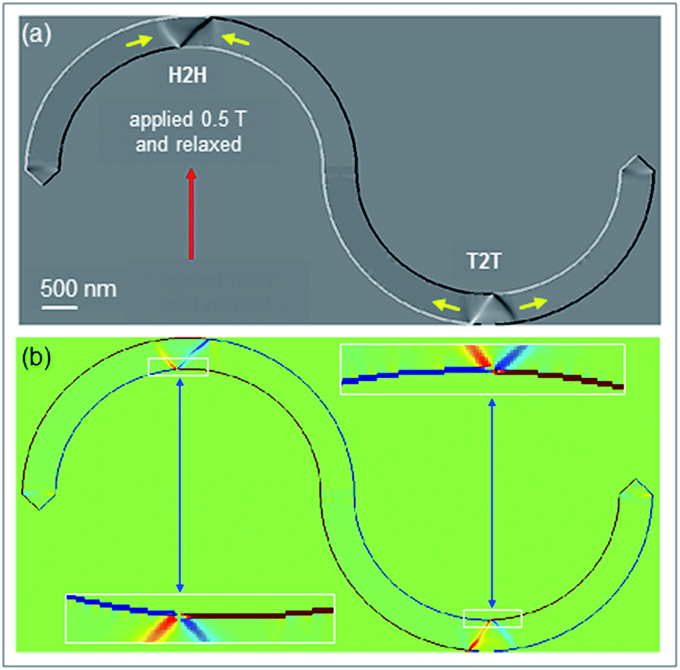 | ||
| Fig. 3 (a) Grey and (b) colour simulated Fresnel images of the 10.5 nm-thick curved nanowire with 500 nm-width at which head-to-head (H2H) and tail-to-tail (T2T) TDWs were simultaneously created by applying an external field of 0.5 T, perpendicular to the easy-axis of the wire. Edge roughness behaviour of the two curvatures of the nanowire are also given in the inset of (b), showing the effect of image pixelation near the wall vertex. | ||
2.2 Parameter definitions
Fig. 4(a) shows spin configuration of a simulated ATDW from the 350 nm-width straight nanowire with a thickness of 21 nm, and its correspondent Fresnel image is shown in Fig. 4(b). Fig. 4(c) describes how to define surface magnetization components and areas within the ATDW. The wall is virtually divided into two halves by drawing a line cross the wire from the wall vertex at the protrusion, highlighted as green (A1) and red (A2) areas in Fig. 4(c). Measurements of two half areas and surface magnetization components within TDWs were realized using MATLAB code.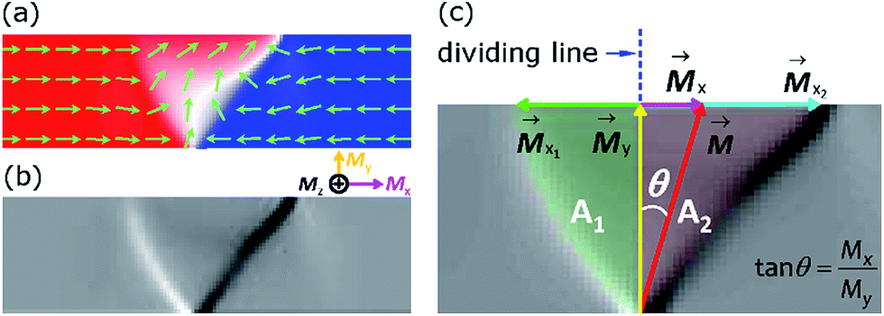 | ||
| Fig. 4 (a) Spin configuration of an ATDW from the 350 nm-width nanowire with a thickness of 21 nm. (b) Simulated Lorentz image of the domain wall showed in (a) with an annotation of magnetization components, Mx, My and Mz. (c) The wall is virtually divided into two areas, A1 and A2, highlighted by green and red backgrounds, respectively. The virtual line is perpendicular to the wire, starting from the wall vertex at the protrusion. Surface magnetization components in those areas are also described. The wall areas and surface magnetization components can be calculated using MATLAB code, and detailed in the text. | ||
A parameter of subtracting the smaller half from the larger one, (A2 − A1), is subsequently defined: if A1 is equal to A2, (A2 − A1) = 0, a STDW is observed, and if A1 is smaller than A2, (A2 − A1) > 0, an ATDW is obtained. To bring nanowires with different widths into comparison, the (A2 − A1) value of each nanowire is normalized by its width, normalized degree of asymmetry in TDW, NDATDW (units in nm). Besides, each simulated OOMMF output file is able to separate into three magnetization components, Mx, My and Mz, as described in the inset of Fig. 4(b). Fresnel images of all simulated structures were calculated, based on the equation, (∇ × M)z = (∂Mx/∂y) − (∂My/∂x), where the image intensity is proportional to curl (M)z in the linear regime of the transfer function.17 Herein, the Mx and My components are only considered. The Mz component does not contribute to the simulated Fresnel image intensity profile. The MATLAB calculation is described in Fig. 4(c): the Mx is the vector sum of Mx1 and Mx2, where Mx1 and Mx2 are surface magnetization vectors which belong to the smaller and larger areas of an ATDW, and in opposite directions. Therefore, if Mx is unequal to zero, the Mx intends to circulate the My into one side of the virtual line, the dashed line in Fig. 4(c). This process creates an ATDW, at which the total magnetization of the ATDW, M, is a vector sum of Mx and My. When Mx1 and Mx2 are equal in magnitude but opposite in sign, this is similar to the case of (A1 = A2), a STDW is obtained in despite of My. Therefore, another parameter is defined by dividing My from Mx, Mx/My ratio. This parameter is proportional to the tangent of the angle (θ) in a right triangle with the opposite and adjacent sides are Mx and My, respectively, as depicted in the inset of Fig. 4(c): if Mx is equal to zero, (Mx1 = Mx2, tan![[thin space (1/6-em)]](https://www.rsc.org/images/entities/char_2009.gif) θ = Mx/My = 0), a STDW is observed, otherwise Mx > 0, an ATDW is obtained. The degree of asymmetry in a TDW is strongly determined by the net surface magnetic moments/spins, Mxi. With the above parameter definitions, we expect that Mx/My ratio will be correlated to (A2 − A1) and/or NDATDW.
θ = Mx/My = 0), a STDW is observed, otherwise Mx > 0, an ATDW is obtained. The degree of asymmetry in a TDW is strongly determined by the net surface magnetic moments/spins, Mxi. With the above parameter definitions, we expect that Mx/My ratio will be correlated to (A2 − A1) and/or NDATDW.
3 Experimental details
The 10.5 nm-thick curved nanowires studied here were formed in two main steps: (1) a continuous 10.5 nm-thick polycrystalline Py film was evaporated onto an electron transparent membrane22 using a thermal evaporator with the evaporation rate of 0.03 nm s−1. The TEM membrane is a 35 nm-thick amorphous Si3N4 film supported on a 500 mm-thick silicon frame with a 100 × 100 mm2 electron transparent window, obtained from TED PELLA, INC. The film thickness was controlled and monitored using a quartz crystal microbalance technique where a correlation between mechanical oscillation and resonant frequency is controlled. The use of the TEM Si3N4 membrane allows us to investigate magnetic properties of the Py film directly from the Lorentz microscope.19 (2) Py nanowires with different widths (from 200 nm to 550 nm, 50 nm steps), as discussed in Subsection 2.1, were patterned using the focused ion beam (FIB) method to isolate these nanowires from the continuous film.21–24 Herein, a FEI Nova NanoLab 200 SEM/FIB workstation consists of a Ga+-ion probe with a full-width half maximum (FWHM) of 10 nm (Eion-energy = 30 keV and Iion-current = 10 pA) was used. The overlap of the two adjacent beam spots is the 50% FWHM. The magnetic characterization was undertaken using the Fresnel imaging mode of a field emission gun CM20 microscope19 with a defocus distance (Δz) of 3.6 mm. To avoid charging during the FIB fabrication and TEM imaging, a very thin conducting Au layer of 10 nm was deposited in the backside of the TEM-Si3N4 membrane using a sputtering deposition. The structure of the fabricated nanowires with different widths is given in Fig. 5 at which bright field (BF) TEM images were particularly recorded at the two curvatures of the 10.5 nm-thick curved nanowires, showing edge roughness behaviour of these nanowires under the FIB ion milling processes.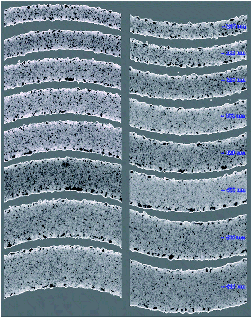 | ||
| Fig. 5 Bright field (BF) TEM images recorded at the two curvatures of the 10.5 nm-thick curved nanowires with different widths. These nanowires were patterned by the focused ion beam (FIB) irradiation method, showing edge roughness behaviour of these nanowires with the FIB milling processes. The images in the right and left panels correspond to the locations where head-to-head (H2H) and tail-to-tail (T2T) DWs will be nucleated with an external field perpendicular to the easy-axis of the wires. | ||
4 Results and discussion
4.1 Simulation results of straight nanowires
As mentioned in Subsection 2.2, MATLAB code was used to calculate the areas and surface magnetization components within the TDWs from the simulated Lorentz images of straight nanowires, as discussed in Fig. 2 and 4. As a result, NDATDW and Mx/My values are plotted for all nanowires with different widths and thicknesses, the so-called wall phase diagrams, as shown in Fig. 6. The transition points between STDWs and ATDWs, denoted as STDWs ↔ ATDWs, achieved by Nakatani et al.,4 are also plotted for a comparison (blue-symbols, ). Within the transition zone, Mx/My and NDATDW both are equal to zero, a STDW is observed, otherwise an ATDW is obtained. The transition points between ATDWs and VDWs,4 denoted as ATDWs ↔ VDWs, are also added (red-symbols,
  ). This does not mean that the DWs with the NDATDW or Mx/My values above the ATDW ↔ VDW points in the wall phase diagrams are VDWs. This is caused by the initial states of these DWs which were all defined as TDW geometries, and these TDWs could reach metastable states. Fig. 6 also shows that the trends of wall transformations in the two wall phase diagrams are similar, and the transition points are in good agreement for all nanowires with different widths. However, NDATDW value slowly increases with increasing nanowire-width, while Mx/My value abruptly increases above the STDW ↔ ATDW zone. This difference of the two wall phase diagrams can be attributed to a difference in functions which mathematically describe Mx/My and NDATDW. The trends of the curves in the wall phase diagrams reflect all of the simulated wall configurations in the straight nanowires.
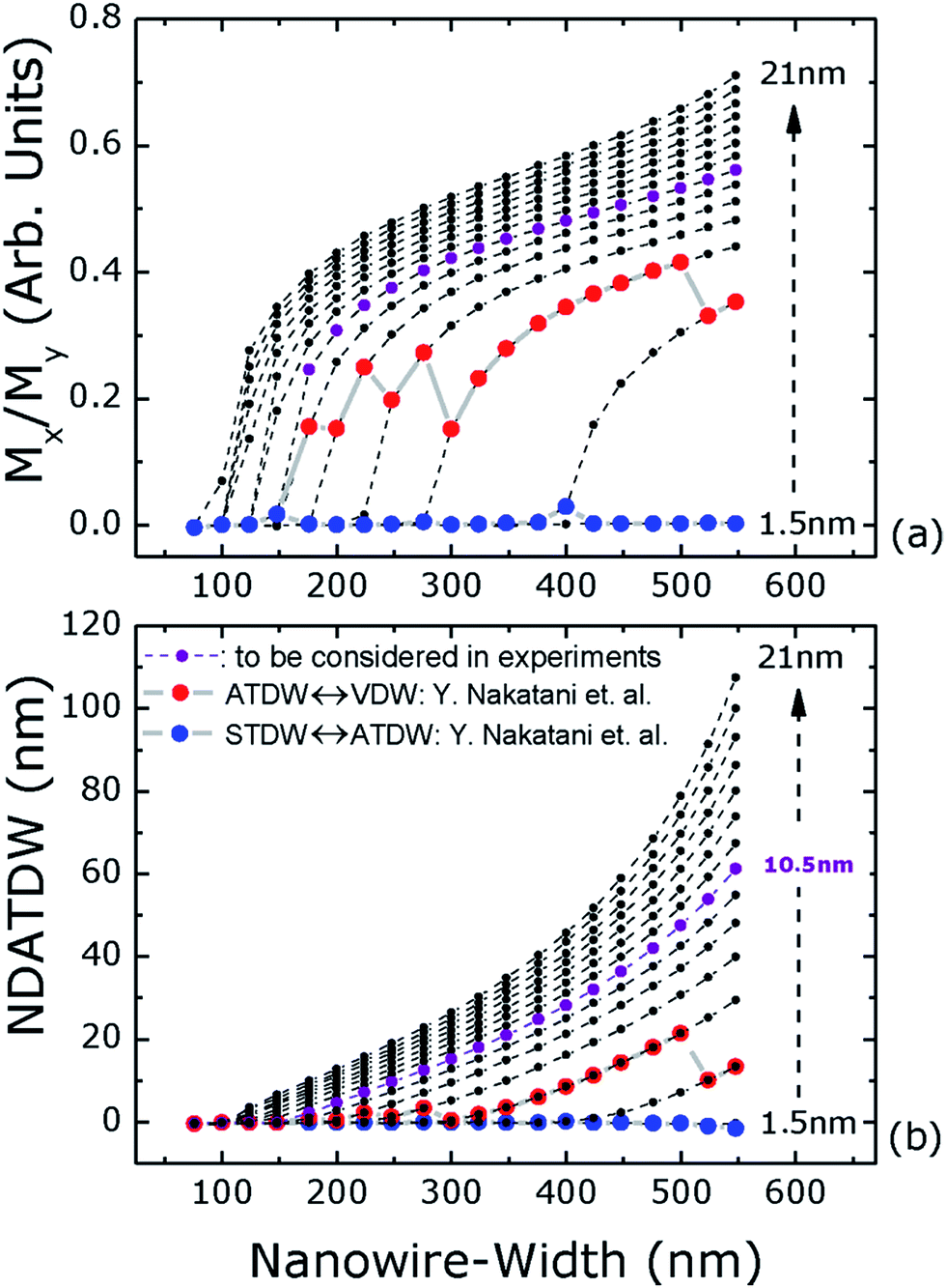 | ||
Fig. 6 Two wall phase diagrams obtained from the simulated Lorentz images of straight nanowires with different widths and thicknesses. Both diagrams primarily describe the transition points between STDWs and ATDWs, denoted as STDWs ↔ ATDWs: (a) ratio of surface magnetization components (Mx/My) and (b) normalized degree of asymmetry in transverse domain wall (NDATDW) values as a function of nanowire-widths with different thicknesses. The red ( ) and blue ( ) and blue ( ) symbols represent the transition points of VDWs ↔ ATDWs and ATDWs ↔ STDWs, respectively, these points are taken from ref. 4. The violet ( ) symbols represent the transition points of VDWs ↔ ATDWs and ATDWs ↔ STDWs, respectively, these points are taken from ref. 4. The violet ( ) symbols particularly describe for the case of the straight nanowires with a thickness of 10.5 nm, this thickness will be considered experimentally in curved nanowires. ) symbols particularly describe for the case of the straight nanowires with a thickness of 10.5 nm, this thickness will be considered experimentally in curved nanowires. | ||
Using the above wall phase diagrams, the degree of asymmetry of a TDW can be estimated by measuring areas or surface magnetization components within the TDW. The correlation between surface magnetic moments/spins and geometrical areas of a TDW is found. The wall phase diagrams are however excluded edge roughness effects.1,3 Such effects might affect both DATDW and Mx/My values. Therefore, understanding this effect is vital for practical applications at which information on the precise transformation mechanism between STDWs and ATDWs is essential. The remaining parts will discuss simulation and experimental results of TDWs which created in the 10.5 nm-thick curved nanowires with different widths, as discussed in Fig. 3 and 5, where the edge roughness is considered as a combination of regular and irregular behaviour resulting from curvatures of the curved structures and FIB milling processes.
4.2 Results of 10.5 nm-thick curved nanowires
The simulated Fresnel images of the 10.5 nm-thick curved nanowires describe purely magnetic contrast, e.g. one of these curved nanowires is given in Fig. 3. These images were calculated from the in-plane magnetization components, Mx and My. The effect of defocus on the contrast of the Fresnel image assumes to be negligible. The edge fringes in those Fresnel images include both magnetic and electrostatic effects. Therefore, domain walls created in the narrow nanowires, i.e. 200 nm, 250 nm and 300 nm-width, might not be clearly seen. Moreover, we assume that effects of edge roughness are negligible in the patterned nanowires. NDATDW values of the walls created in the same curved nanowire are therefore unchanged at different locations. In fact, NDATDW values alter when these walls are created in the same curvature of the wire at different positions. Such changes could be ascribed to the effect of edge roughness. To elucidate further on this issue, an external field with different directions was applied with an angle, θ (θ ≤ 25°) with respect to the direction perpendicular to the easy-axis of the structure, as depicted in Fig. 7.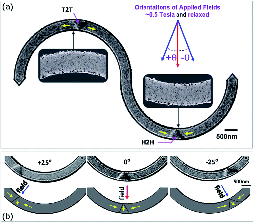 | ||
| Fig. 7 (a) A Fresnel image of the 10.5 nm-thick curved nanowire with a width of 535 nm at a relaxed state. Herein, TDWs were created by applying a 0.5 T 0°-oriented field, as depicted in the top right of the inset. Two bright field (BF) TEM images are also included at the created wall locations. (b) Fresnel images of three relaxed H2H-TDWs which were nucleated in different field orientations, i.e. θ = 0°, ±25°, and schematics of these walls are also given in the lower panel. | ||
Fig. 7 shows TDWs which were created at different positions in a 10.5 nm-curved nanowire, i.e. a Fresnel image of the curved nanowire with a width of 535 nm. H2H and T2T-TDWs were simultaneously created at the two curvatures of the structure by applying a 0.5 T 0°-oriented field, as described in the top right inset of Fig. 7(a). Two bright field (BF) TEM images of these selected areas are also given in Fig. 7(a). Under different external field directions, i.e. 0° and ±25°-oriented fields, Fresnel images recorded at these three H2H DW locations are shown in Fig. 7(b). The geometries of the TDWs nucleated with the 0° and +25°-field orientations are mostly similar. While the TDW created with the −25°-field direction is more asymmetric. These TDW characteristics can be depicted and shown in the lower panel of Fig. 7(b). This also suggests that a TDW can be nucleated by the tilting field and it could be pinned at any pinning sites created at the long edges of the curved nanowire. With the use of different field orientations, the effect of edge roughness can be probed. NDATDW values for TDWs created in different field orientations, i.e. 0°, ±15° and ±25°, were also measured.
Along with the above experimental results, a series of Fresnel images of H2H- and T2T-TDWs was also simulated in the 10.5 nm-thick curved nanowires with different widths, from 200 nm to 550 nm, 50 nm steps, as discussed in Fig. 3. The procedure of DW creations in these curved nanowires is similar to the experimental case, a 0.5 T 0°-field was applied and relaxed. Similar to the case of the straight nanowires, NDATDW values of these simulated H2H-TDWs were then calculated. Taking into account all of the simulation and experiment results of the curved nanowires into the wall phase diagram of the 10.5 nm-thick straight nanowires, as shown in Fig. 6(b). A summary of these results is plotted in Fig. 8. This figure shows that the simulation and experiment NDATDW values of the curved nanowires scatter around the trend of the NDATDW curve of the 10.5 nm-thick straight nanowires. Fresnel images of TDWs created in narrow curved nanowires, i.e. 200 nm and 250 nm-width, are difficult to analyse. This difficulty results from the reduced nanowire-widths. Moreover, a few of experimental NDATDW values are not shown in the wall phase diagram due to those created walls were VDWs. Based on the given results, we can conclude that the effect of edge roughness strongly affects the NDATDW value, and it alters along the two long edges of a nanowire. This effect primarily originates from differences of local spin configurations at the rough edges of any nanowire. Based on the BF TEM images taken at the two curvatures of the 10.5 nm-thick curved nanowires with different widths, as given in Fig. 5 and the inset of Fig. 7(a). These images show that grain size of Py film in the nanowire varies from the centre to the edges of the wire. Some larger grains covered by recrystallization appearing around the edges of the nanowire are due to the FIB irradiation processes that might affect magnetic properties of the entire nanowire.21–28
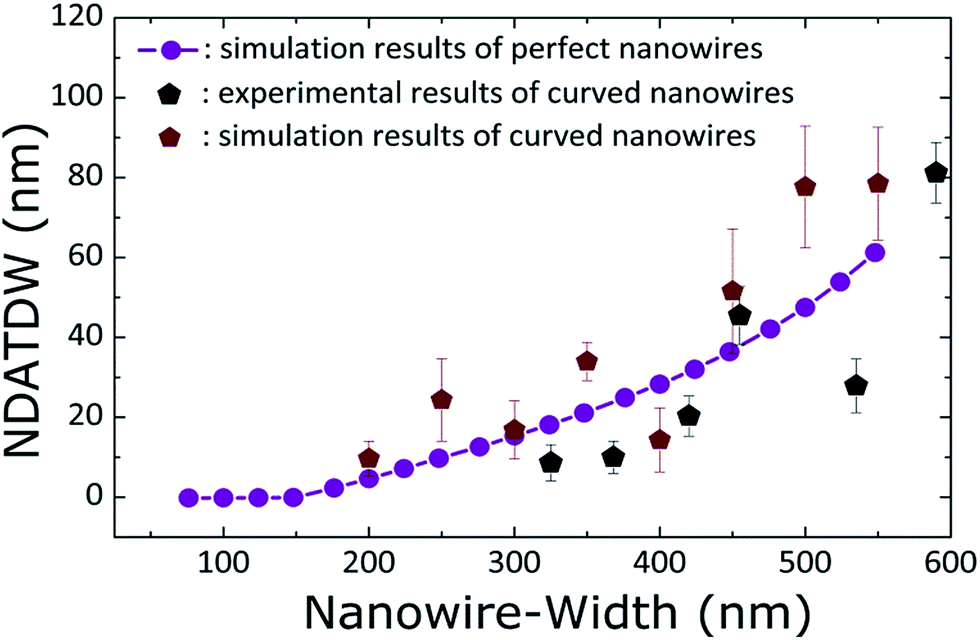 | ||
Fig. 8 A wall phase diagram of the 10.5 nm-thick nanowires with different nanowire-widths for the case of H2H-TDWs. The diagram shows a distribution of simulation and experiment NDATDW values of the curved nanowires in differing nanowire-widths, as presented as red- and dark-solid pentagons. These values scatter around the trend of the simulation results of the 10.5 nm-thick straight nanowires which is reproduced from Fig. 6(b), and graphed as violet solid-circle-dashed line ( ). ). | ||
5 Conclusions
The quantitative measurement of asymmetry in transverse domain walls created in straight and curved polycrystalline Py nanowires was demonstrated. A correlation between the surface magnetization components and geometrical areas within a TDW was also found. The investigated results were summarized and plotted via the two wall phase diagrams with emphasis on the transition between symmetric and asymmetric transverse domain walls. The simulation and experiment results of the 10.5 nm-thick curved nanowires showed that a range of asymmetric wall stability exists. This leads us to conclude that the effect of edge roughness prominently contributes to the degree of asymmetry in TDWs. These results are further supported through BF TEM images, showing that grain sizes of the polycrystalline Py film varied from the two edges to the centre of the nanowire. Using this calculation approach, effects of edge roughness and/or Py quality under fabrication processes for straight and curved Py nanowires can be quantified that is vital for tailoring device properties.Conflicts of interest
There are no conflicts to declare.Acknowledgements
The authors want to thank Dr Damien McGrouther and Dr Sam McFadzean for simulation and experiment assistance, and Dr Stephen McVitie, Dr Donald A. MacLaren, Dr Kerry O'Shea for fruitful discussions on Digital Micrograph, OOMMF and MATLAB calculations. This work was supported by SUPA studentship competition prize (2007–2011).References
- S. S. P. Parkin, M. Hayashi and L. Thomas, Science, 2008, 320, 190–194 CrossRef CAS PubMed.
- D. A. Allwood, G. Xiong, M. D. Cooke, C. C. Faulkner, D. Atkinson, N. Vernier and R. P. Cowburn, Science, 2002, 296, 2003–2006 CrossRef CAS PubMed.
- M. Kläui, J. Phys.: Condens. Matter, 2008, 20, R313001 CrossRef.
- Y. Nakatani, A. Thiaville and J. Miltat, J. Magn. Magn. Mater., 2005, 290–291, 750–753 CrossRef CAS.
- R. D. McMichael and M. J. Donahue, IEEE Trans. Magn., 1997, 33, 4167–4169 CrossRef.
- S. Lamrani, A. Guittoum, R. Schäfer, S. Pofahl, V. Neu, M. Hemmous and N. Benbrahim, Eur. Phys. J.: Appl. Phys., 2016, 74, 30302 CrossRef.
- S. Y. Park, K. M. Lim, J. Namkung, M. C. Kim and C. G. Park, Scr. Mater., 2006, 54, 621–625 CrossRef CAS.
- K. M. Lim, S. Y. Park, J. Namkung, M. C. Kim and C. G. Park, Mater. Sci. Eng., A, 2007, 449–451, 444–447 CrossRef.
- B. Zhang, N.-E. Fenineche, L. Zhu, H. Liao and C. Coddet, J. Magn. Magn. Mater., 2012, 324, 495–500 CrossRef CAS.
- D. Atkinson, D. A. Allwood, C. C. Faulkner, G. Xiong, M. D. Cooke and R. P. Cowburn, IEEE Trans. Magn., 2003, 39, 2663–2665 CrossRef CAS.
- V. Estévez and L. Laurson, Phys. Rev. B, 2016, 93, 064403 CrossRef.
- S. Janićević, L. Laurson, K. J. Måløy, S. Santucci and M. J. Alava, Phys. Rev. Lett., 2016, 117, 230601 CrossRef PubMed.
- I. Rissanen and L. Laurson, Phys. Rev. B, 2016, 94, 144428 CrossRef.
- D. Petit, H. T. Zeng, J. Sampaio, E. Lewis, L. O'Brien, A.-V. Jausovec, D. Read, R. P. Cowburn, K. J. O'Shea, S. McVitie and J. N. Chapman, Appl. Phys. Lett., 2010, 97, 2331021 Search PubMed.
- J. Gadbois and J.-G. Zhu, IEEE Trans. Magn., 1995, 31, 3802–3804 CrossRef.
- J. Gadbois, J.-G. Zhu, W. Vavra and A. Hurst, IEEE Trans. Magn., 1998, 34, 1066–1068 CrossRef.
- S. McVitie and M. Cushley, Ultramicroscopy, 2006, 106, 423–431 CrossRef CAS PubMed.
- C. W. Sandweg, N. Wiese, D. McGrouther, S. J. Hermsdoerfer, H. Schultheiss, B. Leven, S. McVitie, B. Hillebrands and J. N. Chapman, J. Appl. Phys., 2008, 103, 093906 CrossRef.
- J. N. Chapman, J. Phys. D: Appl. Phys., 1984, 17, 623–647 CrossRef CAS.
- K. J. O'Shea, S. McVitie, J. N. Chapman and J. M. R. Weaver, Appl. Phys. Lett., 2008, 93, 202505 CrossRef.
- D. McGrouther, W. A. P. Nicholson, J. N. Chapman and S. McVitie, J. Phys. D: Appl. Phys., 2005, 38, 3348–3353 CrossRef CAS.
- M. A. Basith, S. McVitie, D. McGrouther, J. N. Chapman and M. R. Weaver, J. Appl. Phys., 2011, 110, 083904 CrossRef.
- J. Fassbender and J. McCord, J. Magn. Magn. Mater., 2008, 320, R579–R596 CrossRef.
- Z. M. Wang, FIB Nanostructures, Springer International Publishing, Switzerland, 2013, pp. 171–175 Search PubMed.
- A. F. Pacheco, J. M. de Teresa, A. Szkudlarek, R. Córdoba, M. R. Ibarra, D. Petit, L. O'Brien, H. T. Zeng, E. R. Lewis, D. E. Read and R. P. Cowburn, Nanotechnology, 2009, 20, 475704 CrossRef PubMed.
- H. H. Long, E. T. Ong, T. Liu, H. L. Li, Z. J. Liu, E. P. Li, H. Y. Wu and A. O. Adeyeye, J. Magn. Magn. Mater., 2006, 303, e299–e303 CrossRef CAS.
- W. F. Van Dorp and C. W. Hagen, J. Appl. Phys., 2008, 104, R08130 CrossRef.
- S. Bance, T. Schreft, G. Hrkac, D. Suess, C. Brownlie, S. McVitie, J. N. Chapman and D. Allwood, IEEE Trans. Magn., 2006, 42, 2966–2968 CrossRef CAS.
| This journal is © The Royal Society of Chemistry 2017 |