 Open Access Article
Creative Commons Attribution 3.0 Unported Licence
Thermal transport in graphene/stanene hetero-bilayer nanostructures with vacancies: an equilibrium molecular dynamics study
Asir Intisar Khan a,
Ratul Paul
 b and
Samia Subrina
 *a
*a
aDepartment of Electrical and Electronic Engineering, Bangladesh University of Engineering and Technology, Dhaka, 1205, Bangladesh. E-mail: samiasubrina@eee.buet.ac.bd; ssubr002@ucr.edu; Fax: +880-2-9668054; Tel: +880-19-3795-9083 Tel: +880-2-9668054
bDepartment of Mechanical Engineering, Bangladesh University of Engineering and Technology, Dhaka, 1000, Bangladesh
First published on 19th September 2017
Abstract
In this study, we have performed equilibrium molecular dynamics simulations to model the thermal transport in nanometer sized graphene/stanene hetero-bilayer structures. Our simulations include the computation of thermal conductivity of pristine as well as defected structures containing several types of vacancies namely point vacancy, bi-vacancy and edge-vacancy. The room temperature thermal conductivity of the pristine 10 nm × 3 nm graphene/stanene hetero-bilayer is estimated to be 127.2 ± 13.8 W m−1 K−1. We have studied the impact of temperature and width of the sample on thermal transport in both pristine and defected nanoribbons. Thermal conductivity is found to decrease with the increasing temperature while it tends to increase with the increasing width. Furthermore, we have investigated the thermal conductivity of defected bilayers as a function of vacancy concentration within a range of 0.5% to 2% and compared those for pristine structures. A vacancy concentration of 2% leads to 50–70% reduction in the thermal conductivity of the pristine bilayer nanoribbons. Such a study provides a good insight into the optimization and control of thermal transport characteristics of the low dimensional graphene/stanene nanostructure based thermal and nanoelectronic devices.
1. Introduction
Of late, the technological advancements inspired by graphene1,2 owing to its exceptional combination of several electrical properties,3 high thermal conductivity4 and mechanical strength5 have opened a new research field involving a wide variety of two dimensional (2D) nanomaterials. In fact, other group-IV 2D materials such as silicene, germanene and stanene have received special attention considering their attractive electronic properties and wide application prospects, that range from next generation energy efficient nanoelectronic devices to transparent and flexible electronic systems.Despite the exceptionally high thermal conductivity of single layer graphene materials6,7 (4840 W m−1 K−1 to 5300 W m−1 K−1), the absence of a bandgap8 notably limits their use in the high performance semiconductor based nanoelectronic device applications. On the other hand, recently a new 2D group IV material, stanene which is a buckled honeycomb structure of 2D hexagonal tin film, has driven interest due to its intriguing prospect as quantum Hall insulator,9 topological insulator10 and topological superconductor.11 In addition, stable low buckled form of stanene12 has already been synthesized on the Bi2Te3 (111) substrate13 and is theoretically investigated to support a large-gap 2D quantum spin Hall (QSH) state at room temperature. It thereby enables superior electric conduction with zero dissipation.14,15 However, stanene has a zero bandgap without spin orbiting coupling (SOC).12 In this context, Chen et al.16 has recently reported an opening of ∼77 meV bandgap and an enhanced optical response realized in the most stable stacking configuration of graphene/stanene hetero-bilayer. The structure can be highly promising for application in field effect transistors (FET) which would further require proper thermal management. Consequently, using non-equilibrium molecular dynamics simulation (NEMD), Hong et al.17 studied the thermal conductivity and thermal resistance of the pristine graphene/stanene hetero-bilayer with the variation of length and temperature. But, the estimated thermal conductivity using NEMD simulation is generally smaller than the experimentally obtained results.18 It can be overcome by the use of equilibrium molecular dynamics (EMD) simulation.19 Moreover, size effects in NEMD are more severe than EMD. Therefore, EMD simulation is always a better choice for simulations involving periodic boundary conditions.20
On the other hand, some forms of structural defects and vacancies can certainly be associated during the experimental synthesis, integration and fabrication process of the graphene/stanene hetero-bilayer. In fact, during the crystal growth process using the chemical vapor deposition (CVD) technique, the defects in graphene are created.21 Such defects have significant impact on the chemical, physical as well as thermal properties of materials.22 The presence of several types of defects, dislocations and vacancies can reduce the thermal conductivity of pristine graphene layer and its nanostructures by about 50–80% as reported in the literature.18,23–25 Therefore, from practical perspective, the study on how these defects influence the thermal conductivity of graphene/stanene hetero-bilayer is essential for its proper thermal transport characterization. At the same time, this study would inspire the use of graphene/stanene hetero-bilayer in the efficient thermal management and effective application purpose such as high-speed spintronic devices. Hence, in this work we perform EMD simulations to model the thermal transport of defected graphene/stanene hetero-bilayer structures with various types of vacancies and compare the obtained values with the thermal conductivity of the corresponding pristine nanoribbon structures. Three types of vacancies namely point vacancy, bi vacancy and edge vacancy are considered in our study. The study on the effect of varying temperature and increasing sample width on the thermal conductivity of the defected as well as pristine hetero-bilayer structure has also been carried out. Next, we have analyzed the change in the thermal conductivity of defected hetero-bilayer by varying the defect concentrations. Defect concentrations are defined as the percentage ratio of the number of vacancies to the total number of atoms considered. Finally, phonon density of states (PDOS) i.e. phonon power spectra are computed for both the pristine and defected graphene/stanene hetero-bilayer to analyze the possible correlation of their estimated thermal conductivities.
2. Simulation details
In this study, we have carried out equilibrium molecular dynamics (EMD) simulations using LAMMPS (Large-scale Atomic/Molecular Massively Parallel Simulator)26 for investigating the thermal transport characteristics of graphene/stanene hetero-bilayer nanoribbon. 2nd generation reactive empirical bond order (REBO) potential27 has been considered to model the interactions between C–C bonds in graphene. On the other hand, optimized Tersoff type bond order potential parameters proposed by Cherukara et al.28 have been used to model the Sn–Sn interactions in the stanene layer. Standard 12-6 Lennard-Jones (LJ) potential is used to describe the van der Waals interaction between the graphene and stanene monolayer. LJ potential can be expressed as:
 | (1) |
For the computation of the thermal conductivity, EMD simulation based on linear response theorem has been exercised in this study. In this method, thermal conductivity computation is related to ensemble average of heat current auto correlation function (HCACF) via following Green–Kubo formulation:
 | (2) |
In our study, periodic boundary condition was applied in the zigzag direction. A time step of 0.5 fs was used for the simulations. Equations of atomic motion were integrated using a velocity-Verlet integrator. The structures were equilibrated using the Nose–Hoover thermostat for 3 × 10⁵ time steps followed by NVE ensemble for 105 time steps. Energy minimization is obtained using the steepest decent algorithm. The in-plane heat current data were recorded in every four steps by performing constant energy simulations and HCACF values were calculated by averaging the ten obtained HCACFs. Using eqn (2), a converged value of thermal conductivity has been calculated, as the ensemble average of three independent micro canonical ensemble (constant number of particles, volume and energy) i.e. NVE ensembles, each starting with a different initial condition.
For the calculation of phonon density of states (PDOS), FixPhonon command31 of LAMMPS has been employed to directly obtain the dynamical matrices from MD simulation. Using the dynamical matrices an auxiliary post processing code ‘phana’ was used for the evaluation of PDOS. In this study, alongside the uniform generation of q (wave vector) points, we used a tricubic32 interpolation method to compute the PDOS for both pristine and defected structures.
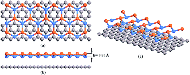
Fig. 1 presents atomistic modeling of a 10 nm × 3 nm sized pristine graphene–stanene hetero-bilayer structure considered in this study. Initial lattice constant of stanene (4.66 Å) is stretched by about 4.7% to generate the configuration as shown in Fig. 1. Chen et al.16 has recently reported this particular configuration to be most stable using DFT. After geometry optimization, lattice constant of graphene is found to be 2.44 Å while optimized lattice constant and buckling height of the lattice matched i.e. stretched stanene are 4.88 Å and 0.85 Å respectively.
Fig. 2 is a pictorial depiction of the hetero-bilayer structure with three types of vacancies namely point vacancy, bi-vacancy and edge vacancy. Point vacancy as shown in Fig. 2(a) originates from the discarding of a single atom randomly from the lattice structures. Bi-vacancy is represented either by the lumping of two consecutive point vacancies or by the random elimination of a pair of bonding atoms as shown in Fig. 2(b). On the other hand, edge vacancy particularly focuses on the removal of single atoms solely from the edge or lattice boundary as shown in Fig. 2(c). In this study, we have separately considered simulation models involving each type of random vacancies in both graphene and stanene layers simultaneously as well as vacancies only in stanene layer and only in graphene layer. However, for the representation purpose, three representative atomistic models of the defected graphene/stanene hetero-bilayer nanoribbon structures with different types of vacancies are shown in Fig. 2. In Fig. 2(a), point vacancy is shown (in both Sn and C layers). In Fig. 2(b), bi-vacancy is presented (in only graphene (C) layer) and in Fig. 2(c), edge vacancy is presented (in only stanene (Sn) layer).
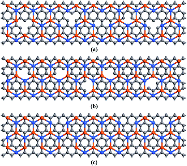 | ||
| Fig. 2 Atomistic models of defected graphene/stanene hetero-bilayer nanoribbon structures with different types of vacancies (a) point vacancy (b) bi-vacancy (c) edge vacancy. | ||
3. Results and discussions
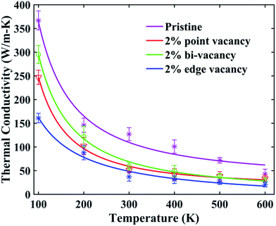
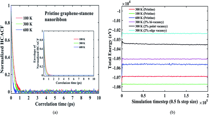
For pristine 10 nm × 3 nm graphene/stanene hetero-bilayer nanoribbon, our computed value of thermal conductivity using EMD at 300 K (room temperature) is 127 ± 13.8 W m−1 K−1. Using NEMD, Hong et al.17 measured the thermal conductivity of 2D graphene/stanene sheet as 311.1 W m−1 K−1 (ref. 17) which is predicted to be decreased with further nanostructuring.28 This is in accordance with our calculated value for the ribbon sized graphene/stanene hetero-bilayer structure. Our obtained thermal conductivity value for the considered hetero-bilayer is significantly higher than some other 2D monolayer structures such as silicene,33 phosphorene34 as well as graphene–MoS2 (ref. 30) hetero-bilayers. Khan et al.35 reported a room temperature thermal conductivity value of ∼2500 W m−1 K−1 for the same sized single layer graphene nanoribbon using second generation REBO potential. In this study, our calculated value of thermal conductivity for the same sized stanene nanoribbon is ∼1.4 W m−1 K−1. It indicates that thermal conductivity of stanene is 3–4 orders of magnitude smaller than that of graphene, further conforming to the literature.28,36,37 This can be attributed to the lower Debye temperature (∼72 K (ref. 36)) of stanene in comparison with graphene (∼1160 K (ref. 37)) and GNRs (322 K (ref. 35)). This significantly low Debye temperature of stanene is originated from the high atomic mass of tin (118.71) and weaker bonding between tin atoms.37Fig. 3 presents the variation of thermal conductivity as a function of temperature for both pristine and defected graphene/stanene bilayer nanoribbon structures. As the figure shows, thermal conductivity decreases exponentially with temperature that ranges from 100 K to 600 K for both pristine and structures with vacancies of several types. This decaying trend is similar to the study by Cherukara et al.28 for stanene and also for both pristine and defected graphene nanoribbons (GNRs).38–40 The drooping characteristic of thermal conductivity indicates the increase of the non-linear thermal resistivity due to phonon–phonon interactions at an elevated temperature.41 Fig. 4(a) can be taken into consideration for the further explanation of the phenomenon observed in Fig. 3. Fig. 4(a) depicts the reasonable decay of the HCACF required for the computation of thermal conductivity using Green–Kubo method. Envelopes of the normalized HCACFs at different temperatures are shown in the figure inset. With the increase in temperature, the number of phonons increases. Consequently phonon–phonon scattering, specifically Umklapp scattering28,36,37 increases. Hence with the increase in temperature, HCACF profile decays to zero in a shorter time38 resulting in the computation of decreasing thermal conductivity. Fig. 4(b) shows the total energy during the simulation for both the pristine and defected bilayer structures at different temperatures. As the figure suggests, energy fluctuations are negligible thereby reflecting the stability of the hetero-bilayer structure with and without defects.
Furthermore, Fig. 3 shows that, percentage decrease of thermal conductivity in defected structure with respect to the pristine structure decreases with the increasing temperature. At elevated temperatures, phonon–phonon scattering surpasses phonon-defect scattering. As a result, the percentage decrease of thermal conductivity at higher temperature is relatively smaller in comparison with that at lower temperature for the defected graphene/stanene hetero-bilayer structure.
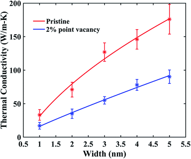
The influence of width on the thermal conductivity of hetero-bilayer structure is studied in Fig. 5. As can be seen from the figure, with the increase in sample width for a fixed length of 10 nm, thermal conductivity increases for both pristine and defected samples. This increasing trend of the thermal conductivity with width is in agreement with the study of Peng et al.36 for stanene nanowires as well as for GNRs.19,38,42 Structure with 2% point vacancy has been considered as a representation of the defected samples. Similar increasing trend with the variation of width is expected in defected structure with other types of random vacancies as well as for other vacancy concentrations.
For the small sized ribbons considered in this study, Fig. 5 shows that with the increasing sample width, at higher widths the increment in thermal conductivity is comparatively lower than the increment of thermal conductivity at smaller widths. This is in agreement with the earlier reported studies.18,19,43 For larger width i.e. for larger sample sizes, greater number of phonons is available for intensifying Umklapp phonon scattering effect. Consequently, thermal conductivity increases at a reduced rate with the increasing width. On the other hand, for smaller sample sizes, phonon boundary scattering mostly dominates the thermal conductivity. In this case, with the increasing width, edge localized phonon scattering effect which is more prevalent than Umklapp scattering, gets suppressed and results in an increased thermal conductivity.19,37,43 Furthermore, using NEMD simulations, Hong et al.17 reported an overall increase of the thermal conductivity of graphene/stanene bilayer sheet for an increasing length. They reported that, thermal conductivity saturates at a value of 267 W m−1 K−1 for 426 nm length at a fixed sample width of 9.7 nm. Hence, our study on the width dependence of thermal conductivity further confirms the increase in the thermal conductivity with the sample size of the graphene/stanene hetero-bilayer ribbons as well as the convergence of thermal conductivity at higher sample dimensions i.e. for sheets.
Experimental synthesis, integration and fabrication process inevitably associate some forms of structural defects and vacancies. Hence, we would now concentrate on the computation of thermal conductivity of the graphene/stanene hetero-bilayer structures with several types of vacancies at various defect concentrations.
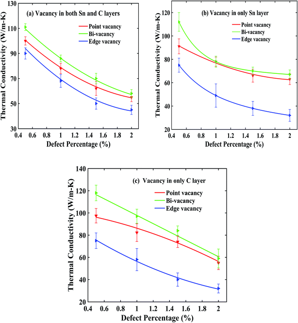
Fig. 6 shows the thermal conductivity of a 10 nm × 3 nm bilayer structure containing several types of vacancies with respect to increasing defect percentage. In Fig. 6(a), we have considered each type of vacancies i.e. point vacancy, bi-vacancy and edge vacancy in both graphene and stanene layers simultaneously. In case of Fig. 6(b), we have carried out the computations for each type of vacancies existing only in stanene layer while Fig. 6(c) presents similar computations for each type of vacancies only in graphene layers. For a random mixed defect (defect in both Sn and C layers) percentage of 0.5%, average room temperature thermal conductivity for the bilayer nanoribbon with point vacancy, bi-vacancy and edge vacancies are ∼100 W m−1 K−1, ∼111 W m−1 K−1 and ∼90 W m−1 K−1, respectively. For all types of vacancies, thermal conductivity decreases exponentially with the increasing defect percentage in each case as depicted in Fig. 6(a)–(c). This phenomenon can be attributed to the localization of low frequency phonons around a vacancy in the structure.25 These low frequency i.e. long wavelength phonons are the majority heat carriers in graphene35 and stanene.37 The localization of these heat carriers in the presence of vacancies reduces the thermal transport capability of the graphene/stanene heterobilayer structure. Moreover, strong inelastic scattering at around the vacancy centers as well as at a distance from the vacancy centers38 causes an overall reduction in the thermal conductivity of the heterobilayer structure with vacancies. It can also be seen from Fig. 6 that, in all the cases, bi-vacancy is found to be less severe in terms of reduction in thermal conductivity. On the contrary, edge vacancy and point vacancies impose a comparatively higher reduction in thermal conductivity. This decreasing trend of thermal conductivity with the increase in defect percentage is in line with the reported literatures for 2D materials such as GNRs.23,24,44 Edge vacancy causes the highest percentage of decrease in the thermal conductivity of graphene/stanene hetero-bilayer nanoribbon because of edge roughness and a greater amount of vacancy induced scattering at the edge of the ribbon. In fact, open edges and edge roughness can critically scatter the heat flux in case of narrow GNRs.45 On the other hand, in the presence of point vacancy in the structure, significant vibrations and scattering are accentuated by the breaking of sp2 bonds.24,46 As a result, thermal conductivity reduces significantly.
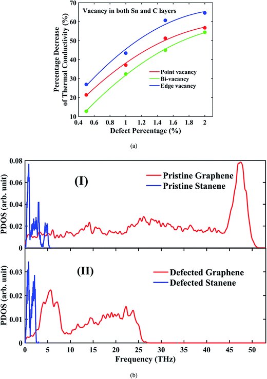
Fig. 7(a) further interprets the percentage decrease in the thermal conductivity of a 10 nm × 3 nm hetero-bilayer structure with different types of random vacancies in comparison with the pristine bilayer of similar size. For a pristine 10 nm × 3 nm graphene/stanene hetero-bilayer, the room temperature average thermal conductivity has been calculated to be ∼127 W m−1 K−1. At a defect concentration of 0.5%, thermal conductivity experiences a reduction of about 10–25% while defect concentration of 2% shows a reduction of about 50–70% from the thermal conductivity (TC) of pristine structure. This is calculated using eqn (3) and interpreted in Fig. 7(a).
 | (3) |
PDOS shown in Fig. 7(b) can be taken into consideration to elucidate this reduction of thermal conductivity in the presence of vacancies in graphene/stanene hetero-bilayer. As the figures suggest, in the high frequency region, the peaks in the PDOS are damped out for the defected structures as opposed to those of pristine structures which is in accordance with the reported literature.23,25,38,47 This phenomenon reduces the mean free path of the corresponding phonon modes. Moreover, there is a shifting of the PDOS towards the low frequency region and some finite peaks appear in the low-frequency regions of the PDOS, as well. This further reduces the phonon relaxation time and mean free path. As a result, an overall decrease in the thermal conductivity occurs. Furthermore, significant phonon scattering around vacancy centers causes a reduction in the phonon mean free path thereby reducing the thermal conductivity.38,48 On the other hand, we observe the presence of high frequency peaks (∼50 THz) in the phonon power spectrum of the graphene layer as opposed to the low frequency peaks (∼3–5 THz) in the stanene layer. It provides further insight into the higher thermal conductivity of the pristine graphene nanostructures with respect to that of the stanene nanostructures.
4. Conclusions
In summary, we have investigated the thermal transport in both the pristine and defected graphene/stanene bilayer nanoribbons using EMD simulations. Computed thermal conductivity of a 10 nm × 3 nm sized pristine bilayer ribbon is 127.2 ± 13.8 W m−1 K−1 which is significantly higher than silicene, stanene, phosphorene and some other 2D monolayers as well as hetero-bilayers. Temperature dependence of thermal conductivity for both pristine and defected configurations shows a decaying trend with the increasing temperature that ranges from 100 K to 600 K. Thermal conductivity is observed to increase with the increasing width and the rate of increment ceases at higher widths, which supports the convergence of thermal conductivity for a higher sample size. Impact of vacancies on the thermal transport of graphene/stanene hetero-bilayer is also comprehensively studied. Thermal conductivity is found to decrease exponentially with the increasing defect concentration. Edge vacancy and point vacancy are more dominant than bi-vacancy in terms of reduction in the thermal conductivity. Significant phonon scattering at and around vacancy centers causes a reduction of the thermal conductivity with vacancies. The damping out of high frequency phonons in our computed phonon power spectra further explains this phenomenon. Apart from providing a deeper insight into the optimization of the thermal transport in novel two dimensional hetero-bilayer structures, our study would encourage the optimal design of the graphene/stanene hetero-bilayer based energy efficient nano-electronic devices.Conflicts of interest
There are no conflicts of interest to declare.References
- A. K. Geim and K. S. Novoselov, Nat. Mater., 2007, 6, 183–191 CrossRef CAS PubMed.
- K. S. Novoselov, A. K. Geim, S. V. Morozov, D. Jiang, Y. Zhang, S. V. Dubonos, I. V. Grigorieva and A. A. Firsov, Science, 2004, 306, 666–669 CrossRef CAS PubMed.
- J. R. Williams, L. Dicarlo and C. M. Marcus, Science, 2007, 317, 638–641 CrossRef CAS PubMed.
- K. Nakada, M. Fujita, G. Dresselhaus and M. S. Dresselhaus, Phys. Rev. B, 1996, 54, 17954–17961 CrossRef CAS.
- C. Lee, X. Wei, J. W. Kysar and J. Hone, Science, 2008, 321, 385–388 CrossRef CAS PubMed.
- A. A. Balandin, S. Ghosh, W. Bao, I. Calizo, D. Teweldebrhan, F. Miao and C. N. Lau, Nano Lett., 2008, 8, 902–907 CrossRef CAS PubMed.
- S. Ghosh, W. Bao, D. L. Nika, S. Subrina, E. P. Pokatilov, C. N. Lau and A. A. Balandin, Nat. Mater., 2010, 9, 555–558 CrossRef CAS PubMed.
- G. Gui, J. Li and J. Zhong, Phys. Rev. B, 2008, 78, 1–6 CrossRef.
- M. Ezawa, J. Supercond. Novel Magn., 2015, 28, 1249–1253 CrossRef CAS.
- S. Rachel and M. Ezawa, Carbon, 2013, 195303, 460–470 Search PubMed.
- S. Li, C. De Cruz, Q. Huang, Y. Chen, J. W. Lynn, J. Hu, Y. Huang, F. Hsu, K. Yeh, M. Wu and P. Dai, J. Am. Chem. Soc., 2011, 5, 3779–3787 Search PubMed.
- B. van den Broek, M. Houssa, E. Scalise, G. Pourtois, V. V. Afanas'ev and A. Stesmans, 2D Mater., 2014, 1, 21004 CrossRef.
- F.-F. Zhu, W.-J. Chen, Y. Xu, C.-L. Gao, D.-D. Guan, C.-H. Liu, D. Qian, S.-C. Zhang and J.-F. Jia, Nat. Mater., 2015, 14, 1020–1025 CrossRef CAS PubMed.
- D. Wang, L. Chen, X. Wang, G. Cui and P. Zhang, Phys. Chem. Chem. Phys., 2015, 17, 26979–26987 RSC.
- Y. Xu, B. Yan, H. J. Zhang, J. Wang, G. Xu, P. Tang, W. Duan and S. C. Zhang, Phys. Rev. Lett., 2013, 111, 1–5 Search PubMed.
- X. Chen, R. Meng, J. Jiang, Q. Liang, Q. Yang, C. Tan, X. Sun, S. Zhang and T. Ren, Phys. Chem. Chem. Phys., 2016, 18, 16302–16309 RSC.
- Y. Hong, C. Zhu, M.-G. Ju, J. Zhang and X. C. Zeng, Phys. Chem. Chem. Phys., 2017, 19, 6554–6662 RSC.
- D. Yang, F. Ma, Y. Sun, T. Hu and K. Xu, Appl. Surf. Sci., 2012, 258, 9926–9931 CrossRef CAS.
- W. J. Evans, L. Hu and P. Keblinski, Appl. Phys. Lett., 2010, 96, 1–3 CrossRef.
- M. H. Khadem and A. P. Wemhoff, Comput. Mater. Sci., 2013, 69, 428–434 CrossRef CAS.
- D. Zhang, B. Hu, D. Guan and Z. Luo, Catal. Commun., 2016, 76, 7–12 CrossRef CAS.
- D. Liu, P. Yang, X. Yuan, J. Guo and N. Liao, Phys. Lett. A, 2015, 379, 810–814 CrossRef CAS.
- B. Mortazavi and S. Ahzi, Carbon, 2013, 63, 460–470 CrossRef CAS.
- J. Haskins, A. Kinaci, C. Sevik, H. Sevinçli, G. Cuniberti and T. Çaǧin, ACS Nano, 2011, 5, 3779–3787 CrossRef CAS PubMed.
- J. J. Yeo, Z. Liu and T. Y. Ng, Nanotechnology, 2012, 23, 385702 CrossRef PubMed.
- S. Plimpton, J. Comput. Phys., 1995, 117, 1–19 CrossRef CAS.
- D. W. Brenner, O. A. Shenderova, J. A. Harrison, S. J. Stuart, B. Ni and S. B. Sinnott, J. Phys.: Condens. Matter, 2002, 14, 783–802 CrossRef CAS.
- M. J. Cherukara, B. Narayanan, A. Kinaci, K. Sasikumar, K. Gray, M. K. Y. Chan and S. K. R. S. Sankaranarayanan, J. Phys. Chem. Lett., 2016, 7, 3752–3759 CrossRef CAS PubMed.
- A. K. Rappe, C. J. Casewit, K. S. Colwell, W. A. Goddard III and W. M. Skiff, J. Am. Chem. Soc., 1992, 114, 10024–10035 CrossRef CAS.
- B. Liu, F. Meng, C. D. Reddy, J. A. Baimova, N. Srikanth, S. V. Dmitriev and K. Zhou, RSC Adv., 2015, 5, 29193–29200 RSC.
- L. T. Kong, Comput. Phys. Commun., 2011, 182, 2201–2207 CrossRef CAS.
- F. Lekien and J. Marsden, Int. J. Numer. Meth. Eng., 2005, 63, 455–471 CrossRef.
- X. Zhang, H. Xie, M. Hu, H. Bao, S. Yue, G. Qin and G. Su, Phys. Rev. B, 2014, 89, 1–7 Search PubMed.
- W. Hu and J. Yang, J. Phys. Chem., 2015, 119, 20474–20480 CAS.
- A. Intisar Khan, I. Ahmed Navid, M. Noshin, H. M. Ahsan Uddin, F. Ferdous Hossain and S. Subrina, Electronics, 2015, 4, 1109–1124 CrossRef.
- B. Peng, H. Zhang, H. Shao, Y. Xu, X. Zhang and H. Zhu, Sci. Rep., 2016, 6, 20225 CrossRef CAS PubMed.
- A. S. Nissimagoudar, A. Manjanath and A. K. Singh, Phys. Chem. Chem. Phys., 2016, 18, 14257–14263 RSC.
- M. Noshin, A. I. Khan, I. A. Navid, H. M. A. Uddin and S. Subrina, AIP Adv., 2017, 7, 15112 CrossRef.
- S. J. Mahdizadeh and E. K. Goharshadi, J. Nanopart. Res., 2014, 16, 1–12 CrossRef CAS.
- J. Zhang and X. Wang, Nanoscale, 2013, 5, 11598–11603 RSC.
- D. J. Ecsedy and P. G. Klemens, Phys. Rev. B, 1977, 15, 5957–5962 CrossRef CAS.
- Y. Hong, L. Li, X. C. Zeng and J. Zhang, Nanoscale, 2015, 7, 6286–6294 RSC.
- H. Cao, Z. Guo, H. Xiang and X. Gong, Phys. Lett. A, 2011, 376, 525–528 CrossRef.
- E. Y. Zhang, Y. G. Chen and Y. B. Tang, Mater. Chem. Phys., 2011, 127, 1–6 CrossRef CAS.
- D. L. Nika, E. P. Pokatilov, A. S. Askerov and A. A. Balandin, Phys. Rev. B, 2009, 79, 1–12 CrossRef.
- W. Zhao, Y. Wang, Z. Wu, W. Wang, K. Bi, Z. Liang, J. Yang, Y. Chen, Z. Xu and Z. Ni, Sci. Rep., 2015, 5, 11962 CrossRef PubMed.
- H. Zhang, G. Lee and K. Cho, Phys. Rev. B, 2011, 84, 1–5 Search PubMed.
- F. Hao, D. Fang and Z. Xu, Appl. Phys. Lett., 2011, 99, 2011–2014 Search PubMed.
| This journal is © The Royal Society of Chemistry 2017 |

