
 Open Access Article
 This Open Access Article is licensed under a
 Creative Commons Attribution 3.0 Unported Licence
Highly efficient UV-sensing properties of Sb-doped ZnO nanorod arrays synthesized by a facile, single-step hydrothermal reaction†
Donghyung Kima,
Wuseok Kimb,
Sangmin Jeon b and
Kijung Yong*a
b and
Kijung Yong*a
aSurface Chemistry Laboratory of Electronic Materials, Department of Chemical Engineering, Pohang University of Science and Technology (POSTECH), Pohang 790-784, Korea. E-mail: kyong@postech.ac.kr
bSmart Materials Sensors Laboratory, Department of Chemical Engineering, Pohang University of Science and Technology (POSTECH), Pohang 790-784, Korea
First published on 21st August 2017
Abstract
The synthesis of electrical and optical property-modulated, low-dimensional metal oxide semiconductors has been adopted for the development of nanodevices. However, conventional modulation methods, such as doping and alloying, generally require rather complex processes, such as multi-step high-temperature reactions, gas-phase growth, high-vacuum processes, etc. Alternatively, in the current study, the facile and cost-effective synthesis of Sb-doped ZnO nanorod arrays (NRAs) is achieved using a simple hydrothermal growth process at 95 °C. Through a single-step reaction, Sb atoms are substitutionally doped at the Zn atom sites with control of the Sb concentration. Sb dopants and Sb-induced oxygen vacancies increase the electron concentration in the ZnO NRAs, enhancing the electrical conductivity of the ZnO NRAs and inducing the further adsorption of ambient oxygen molecules on the nanorod surface. Upon UV irradiation of the highly oxygen-adsorbed, Sb-doped ZnO NRAs, the desorption of oxygen induces greater conductivity changes compared to the undoped samples. Based on this enhanced resistivity change, UV sensor devices were fabricated, and an improved reversible UV sensing performance was observed, with a ∼9-fold enhancement in the photocurrent of the ZnO NRAs after Sb doping. Moreover, UV sensing is achieved even under an extremely low bias of 10–6 V, suggesting the promising application of this material in extremely low-power UV sensor devices.
Introduction
One-dimensional metal-oxide nanomaterials have recently attracted great attention as building blocks in the fabrication of various nanodevices, such as field-effect transistors,1 field electron emitters,2 photovoltaics,3 photoelectrochemical (PEC) energy devices,4,5 gas sensors,6,7 resistive memories,8,9 and photodetectors.10–12 In particular, ZnO nanorods are promising for application in nanoscale UV laser diodes and sensors due to their direct wide bandgap (3.37 eV) and large exciton binding energy (60 meV).13,14 In addition, ZnO nanorod sensors exhibit fast response times and high sensitivity due to their high surface-to-volume ratios.10Recently, the doping of ZnO nanorods has been investigated to manipulate their electrical, optical, and photoconductive properties to enhance their sensing performance for gases or ultraviolet detection.15,16 Various transition metal dopants have been tested for these purposes, such as aluminum (Al),11,12 cobalt (Co),17 gallium (Ga),18 silver (Ag),19,20 copper (Cu),21 antimony (Sb),20,22–24 indium (In),25 and etc. The effects of doping on the sensing properties have been discussed from several points of view.16,17 Upon doping, the carrier concentration of ZnO nanostructures can be improved due to the substitution of metal ions at the Zn2+ sites, which creates additional free carriers.17 This enhanced carrier density leads to enhanced photocurrent generation for UV detection. The higher concentration of carriers can also adsorb more oxygen molecules to form chemisorbed oxygen, which is known to govern the UV photosensing mechanism of ZnO. However, when metal ions are doped at interstitial positions instead of substitutional positions, the free electron concentration will decrease, negatively affecting the sensing properties.26 In addition to these effects, the doping of semiconductor nanorods to adjust the position of the Fermi level may also be utilized to promote molecular adsorption on the surface. Although several studies have reported the enhanced sensing performance of doped ZnO nanostructures, the underlying mechanism is still controversial.
Earlier doping studies of ZnO thin films or nanostructures have applied conventional vapor-phase methods, including chemical vapor deposition (CVD),27,28 molecular beam epitaxy (MBE),29–31 and thermal evaporation.32 Aqueous solution based semiconductor doping under 100 °C is started more recently than vapor, or gas based doping like CVD, MBE, etc.,33,34 including the case of ZnO.35,36 Compared to vacuum gas-phase growth, low-temperature solution reactions have several advantages, such as lower processing cost, large scalability, low thermal budget, and easier use of the source materials. The solution growth of doped ZnO NRs has been recently reported by quite many research groups and the control of the morphology and material properties is also studied including antimony doped ZnO.20,23,37–39 Photosensor applications based on solution-prepared, doped ZnO NRs are also studied several times.16,40
In the current study, vertically aligned ZnO nanorod arrays (NRAs) with Sb-doping were successfully fabricated on ZnO-buffer layer/FTO glass substrates using low-temperature hydrothermal reaction. The Sb-doping concentration was controlled in the ZnO NRAs by adjusting the metal (Zn, Sb) precursor concentration ratio in specific range (under 13% of Sb to Zn ion) in the aqueous ammonia reaction solution.23 XPS, XRD, SIMS and TEM analysis of the Sb-doped ZnO NRs confirmed the high crystallinity of the doped samples. Sb atoms were found to be substitutionally doped into Zn atom sites, enhancing the electron concentration of the ZnO NRAs and attracting more oxygen molecules for adsorption. Due to these effects, our simple photosensors based on Sb-doped ZnO NRAs exhibited a remarkably improved UV response compared to that of undoped ZnO NRAs. Additionally, our Sb-doped ZnO NRAs showed self-powered UV detecting properties under almost zero-biased (∼10–6 V) conditions.
Experiment
Preparation of the Sb-doped ZnO nanorod arrays (NRAs)
Sb-Doped ZnO nanorod arrays (NRAs) were grown on F-doped tin oxide (FTO) film/glass substrates using a simple hydrothermal synthesis method. First, a ∼30 nm thick ZnO seed layer was deposited on the FTO film by RF magnetron sputtering at 8 mTorr of Ar pressure and 100 W of power. Before seed-layer sputtering, the FTO film/glass substrate was sequentially cleaned with distilled water, acetone, and ethanol using a sonicator. Then, the substrate with the seed layer was immersed in a 100 ml aqueous solution containing 10 mM Zn(NO3)2·6H2O with different concentrations (0.1 mM and 1.0 mM) of SbCl3. Then, 3.7 ml of a 30 wt% ammonium hydroxide solution was added to the reaction solution. The hydrothermal reaction proceeded for 12 hours at 95 °C. After growth, the substrates were washed with distilled water and dried in an oven.41Material characterization
Scanning electron microscopy (SEM) images of the synthesized ZnO NRA samples were acquired with an SEM XL30S FEG (5 keV). Energy-dispersive spectroscopy (EDS) analysis using SEM was operated at 20 keV. Undoped and Sb-doped ZnO NRAs were characterized with a high-resolution X-ray diffractometer (D/MAX-2500) operated at 40 kV and 100 mA. Transmission electron microcopy (TEM) data were acquired with a TEM JOEL JEM-2200FS (with image Cs-correction) to obtain low-resolution and high-resolution TEM images, selected-area electron diffraction (SAED) patterns, and electron energy-loss spectroscopy (EELS) data. Secondary-ion mass spectrometry (SIMS) was used to obtain the elemental concentration depth profiles of the ZnO NRA samples using a Cs+ gun (15 keV, 30 nA) with a raster size of 150 μm × 150 μm. The chemical binding states of the ZnO NRAs were analyzed using X-ray photoelectron spectroscopy (VG Scientific ESCALAB 250). The charging condition of the samples was corrected using carbon as the binding energy reference (C 1s peak at 285 eV). The two O 1s peaks of the undoped and Sb-doped ZnO samples were fitted with Gaussian–Lorentzian functions at 530.5 and 531.8 eV, which correspond to ZnO lattice oxygen (LO, Zn–O bond) and oxygen vacancies or defects (VO), respectively. Mott Schottky plot is obtained using IVIUM potentiostat with three electrode potentiostat system in 0.5 M Na2SO4 aqueous solution. Pt mesh, and saturated calomel electrode is used as counter electrode, and reference electrode, respectively. The Mott Schottky analysis is conducted in dark condition at a frequency of 10 kHz.Fabrication of a UV photodetector device with ZnO NRAs and sensor measurements
To examine the UV photodetection properties of the undoped and Sb-doped ZnO NRAs, photodetector devices with an Ag/FTO/ZnO NRA/Ag structure were fabricated by the thermal evaporation of Ag electrode dots on hydrothermally grown ZnO NRAs and FTO glass. The detailed fabrication process is described as follows. First, ZnO NRAs were grown on the patterned seed layers of ZnO on FTO glass. The FTO surface was rubbed with a cotton swab wet by dilute piranha solution to improve the FTO–Ag contact by removing the ZnO sediment formed during the hydrothermal growth process. The area of grown ZnO NRAs is 0.25 cm2 (0.5 cm × 0.5 cm), which was patterned at seed layer deposition stage. The sample was then washed with distilled water again. The sample was covered with a shadow mask to pattern Ag electrode circles with diameters of 400 μm by thermal evaporation. Then, 500–800 nm-thick Ag dot electrodes were deposited on the FTO and ZnO NRAs (see Fig. S1(b) of the ESI†). Before the Ag electrode is deposited, 30 μl of PEDOT:PSS (poly(3,4-ethylenedioxythiophene):poly(styrenesulfonate), 1.3 wt% dispersion in H2O, conductive grade, Aldrich) was spin coated at 3000 rpm for 1 minute on grown Sb-doped ZnO-B NRAs, and was allowed to dry at 95 °C for 1 hour.42 In result, 1 μm-thick PEDOT:PSS layer is deposited on Sb-doped ZnO NRAs (in Fig. S1(b) of the ESI†).The electrical properties of the fabricated ZnO nanorod photodetectors were measured using a Keysight B2902A Precision Source/Measure Unit probe station (MST-4000). The light source for the photoresponse experiment was a UV lamp (UVItec LF-215LM, 365 nm, 16 μW cm−2). The reversible switching properties of the undoped and Sb-doped ZnO NRAs between the low- and high-conductivity state were measured by switching the UV lamp on and off with a constant applied voltage of 0.5 V. The zero-biased reversible switching of ZnO NRAs was also investigated with an applied 10−6 V.
Results and discussion
Fig. 1(a) and (h) shows SEM images of the undoped and Sb-doped ZnO nanorod arrays (NRAs), respectively. The cross-sectional morphology indicates that vertically aligned, high-density ZnO NRAs were grown by the hydrothermal method on the FTO glass substrate. An individual ZnO nanorod has a length of approximately 5 μm and a diameter of 70–100 nm. The size of the ZnO nanorod is controlled by the reaction time in the zinc nitrate solution and the amount of ammonia solution.41 The inset of Fig. 1(a) and (h) shows the top view of the ZnO NRAs. The undoped ZnO NRA, shown in the inset of Fig. 1(a), appears to be denser than the Sb-doped ZnO NRA, shown in Fig. 1(h), because Sb3+ ions may inhibit growth and compete with Zn2+ during growth of the ZnO NRs. Fig. 1(b) and (i) shows TEM bright-field images of an individual undoped and Sb-doped ZnO nanorod, respectively. Both nanorods have a smooth surface with increased diameter toward bottom, giving them a tapered shape. Fig. 1(c) and (d) gives the HRTEM image and SAED pattern of an undoped ZnO NR, respectively, which indicate that an individual ZnO nanorod is single crystalline with a Wurtzite structure grown along the 〈0 0 0 1〉 c-axis growth direction. Upon Sb doping, the crystal structure of the Sb-doped ZnO NR is not changed in HRTEM image and SAED pattern, as shown in Fig. 1(j) and (k). Fig. 1(e)–(g) gives the electron energy-loss spectroscopy (EELS) elemental mappings of Zn, O, and Sb for a single undoped ZnO nanorod, respectively. The signals of Zn and O are clearly observed at the corresponding positions of the ZnO NR, while the Sb elemental signal is at the noise level. In contrast, the EELS signals in Fig. 1(l)–(n), obtained from the elemental mappings of Zn, O, and Sb of a single Sb-doped ZnO nanorod, clearly show a uniform distribution of Sb in the ZnO nanorod.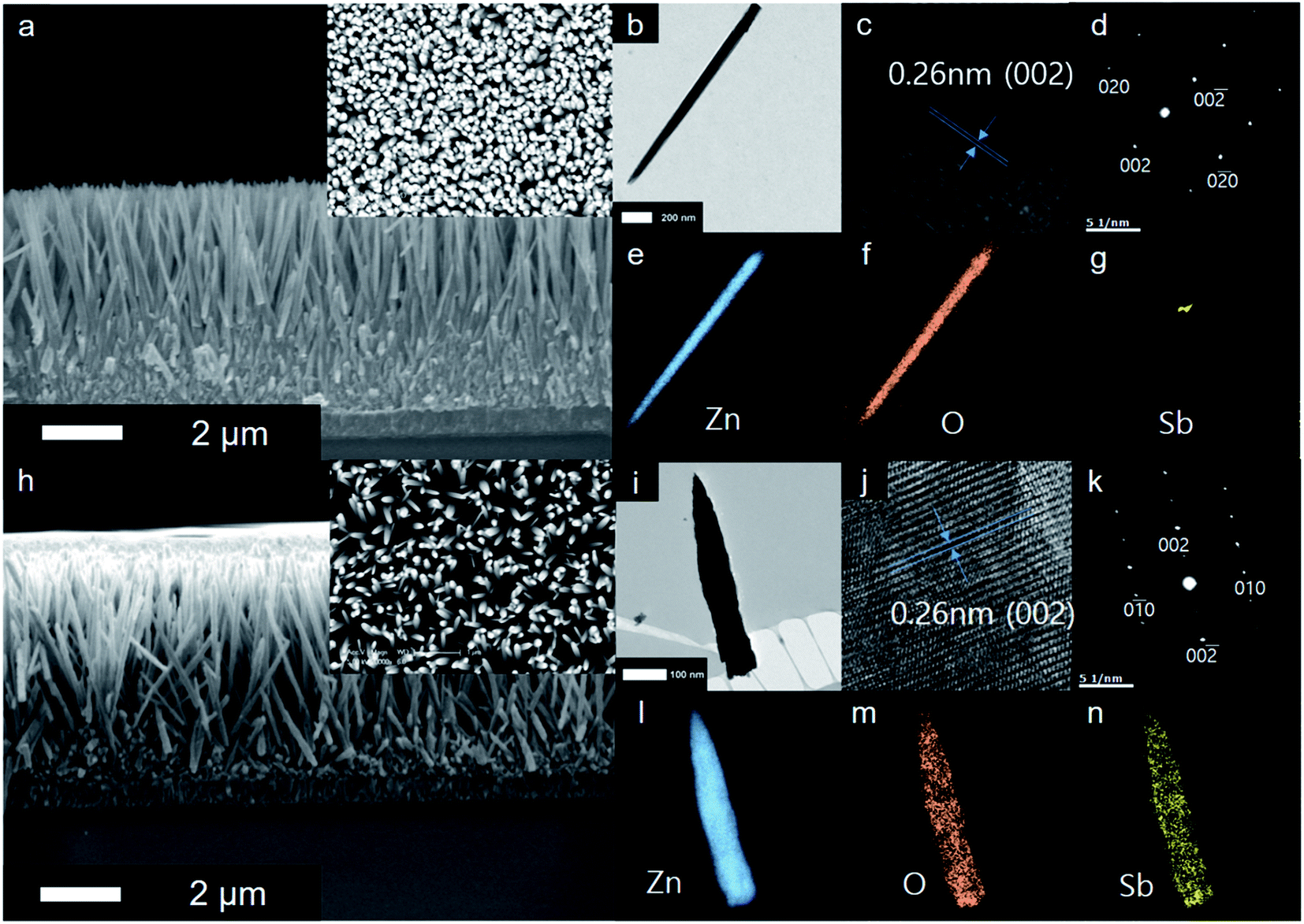 | ||
| Fig. 1 (a, h) Cross-sectional scanning electron microscope images of the undoped and Sb-doped ZnO NRAs, respectively. Insets of (a, h) show the top-view images. (b–g) Transmission electron microscope data of an undoped ZnO NR: (b) TEM, (c) HRTEM, (d) SAED, and (e–g) EELS elemental mapping of Zn, O, and Sb, respectively. (i–n) TEM data of a Sb-doped ZnO nanorod: (i) TEM, (j) HRTEM, (k) SAED, and (l–n) EELS elemental mapping of Zn, O, and Sb, respectively. | ||
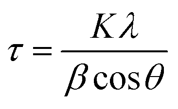
The crystallinity of the undoped and Sb-doped ZnO NRAs was investigated by XRD measurements, and the results are shown in Fig. 2(a). Both samples showed similar XRD patterns, with the most dominant peak at 34.6° corresponding to ZnO (002) (JCPDS 36-1451). These results indicate that both NRs preferentially grow along the c-axis crystal plane of the ZnO Wurtzite structure. No noticeable shift in the XRD peak position is found after Sb doping, which is consistent with the TEM results. The (002) peak of the undoped ZnO NRA (at 34.6°, black line in Fig. 2(a)) has smaller full width at half maximum (FWHM) of 0.355 than the Sb-doped ZnO NRA of 0.414 (at 34.6°, red line in Fig. 2(a)). The FWHM is inversely proportional to the crystalline mean grain size based on the Scherrer equation, written as following eqn (1):
 | (1) |
 | ||
| Fig. 2 (a) X-ray diffraction patterns of the undoped and Sb-doped ZnO NRAs. The full width at half maximum (FWHM) of the (002) peak of the undoped and Sb-doped ZnO NRAs is 0.355 and 0.414, respectively. (b) Secondary-ion mass spectrometry (SIMS) elemental concentration depth profiles (Cs+ gun, 15 keV, 30 nA) for the Sb ions of 3 different ZnO NRA samples (undoped ZnO, Sb-doped ZnO-A, and Sb-doped ZnO-B). | ||
The Sb content in the Sb-doped ZnO NRAs was quantified by secondary-ion mass spectrometry (SIMS) measurements. Fig. 2(b) shows the SIMS elemental concentration depth profiles of the undoped ZnO NRA and Sb-doped ZnO NRA prepared at two different Sb precursor molar ratios. Molar ratios of 0.01 and 0.1 for the Sb source to Zn source were studied for control experiments of the dopant concentration. The two samples were denoted Sb-doped ZnO-A (molar ratio of 0.01) and Sb-doped ZnO-B (molar ratio of 0.1). The depth profiles confirm the similar length of the ZnO NRs of ∼5 μm. The undoped ZnO NRA shows Sb signals at the noise level, as expected, while the Sb-doped ZnO NRAs show two different concentration profiles depending on Sb precursor concentration. Because the SIMS target in the current study is not a film but instead a nanorod structure, the concentration profiles show an unsteady curve the along depth. Sb-Doped ZnO-B shows a Sb concentration approximately 2 times higher than that of Sb-doped ZnO-A. These results indicate that the Sb dopant concentration increases with increasing Sb/Zn precursor molar ratio but is not directly proportional to the Sb precursor concentration in the hydrothermal reaction solution. This is due to the relative chemical reaction activities of the Zn and Sb precursors, which have different metal–ligand binding energies. According to our hydrothermal doping experiments, the upper limit of the antimony concentration for the hydrothermal growth of ZnO nanorods is approximately 12–13% of that of zinc ions. A molar ratio of Sb precursor to Zn source of over 13% is found to hinder the growth of ZnO NRAs.
The chemical binding states of the component elements in the undoped and Sb-doped ZnO NRAs were characterized by XPS, and the results are presented in Fig. 3. Fig. 3(a) shows the XPS spectra of the Zn 2p core level region for the undoped and Sb-doped ZnO NRAs. The spectra are fitted with two peaks at 1021.9 and 1044.9 eV corresponding to the Zn 2p3/2 and Zn 2p1/2 core levels of Zn–O bonding, respectively. There is no difference in the Zn 2p peaks of the undoped and Sb-doped ZnO NRAs. This implies that there is no change in atoms bound to Zn and Zn is only bound to O in Zn–O bonds. Sb atoms can substitute lattice sites of Zn in the ZnO Wurtzite structure and to bind with oxygen during hydrothermal growth, or they can be interstitially doped into the ZnO nanorods. The XPS spectra of the Sb 3d3/2 core level (538–545 eV region of the binding energy) are shown in Fig. 3(b). As expected, a Gaussian-shaped peak is observed for the Sb-doped ZnO NRA sample, while no Sb peak is found for the undoped sample. Moreover, the maximum position of the Gaussian peak (at 540 eV) is shifted to higher binding energy compared to that of metallic Sb (approximately 538 eV). This observation clearly shows that Sb atoms are in their oxidized states and substitute Zn, instead of interstitial doping or substituting O atoms. Based on this, the doping mechanism can be suggested to be the following reaction formula: Zn2+ + Sb → Zn + Sb3+ + e−. Under this condition, Sb-doping will enhance the electron density and conductivity of the ZnO NRAs. The O 1s XPS peaks of the as-prepared ZnO and Sb-doped ZnO NRAs are shown in Fig. 3(c) and (d), respectively. In Fig. 3(c), the O 1s peak of the undoped ZnO NRA is deconvoluted into two Gaussian curves corresponding to ZnO lattice oxygen (530.5 eV) and oxygen vacancies (531.8 eV), respectively.43 Oxygen vacancies are natively generated in pristine ZnO nanorods during growth or vacuum annealing treatment, following the reaction formula: O2− → VO + 2e−.44,45 The native oxygen vacancies supply electron donors to ZnO, making it an n-type semiconductor. The lattice oxygen peak (the red line) is more intense than the oxygen vacancy peak (the green line). For the Sb-doped ZnO sample, shown in Fig. 3(d), a new sub-peak is observed at 530.6 eV corresponding to the Sb 3d5/2 core level (the azure line) due to Sb doping, in addition to the peaks for the lattice and vacant oxygen states. The binding energy of the Sb 3d5/2 core level overlaps with that of lattice oxygen. After deconvolution of the O 1s XPS peak of the Sb-doped ZnO NRAs into three sub-peaks, we found that the oxygen vacancy core level at 531.8 eV is more intense than that of the undoped sample. This implies that Sb doping treatment creates more oxygen vacancies in the ZnO NRAs, because the substitution of larger-sized Sb ions to the Zn ion sites causes structural defects in the Wurtzite ZnO crystal. As a result, Sb atoms doped into the ZnO NRA acts as an electron donor and, at the same time, induces more oxygen vacancies, which generates more electron donors.
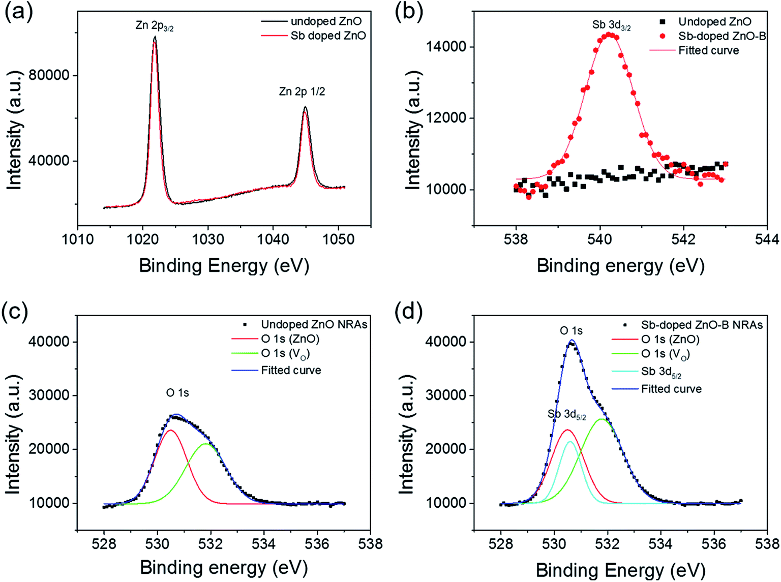 | ||
| Fig. 3 X-ray photoelectron spectroscopy (XPS) of (a) Zn 2p and (b) Sb 3d. (c) Deconvoluted O 1s spectra of the undoped ZnO NRA with two components at 530.5 and 531.8 eV corresponding to lattice oxygen and oxygen vacancies, respectively. (d) Deconvoluted O 1s spectra of the Sb-doped ZnO-B NRA. The additional peak at 530.6 eV corresponds to the Sb 3d5/2 core level. | ||
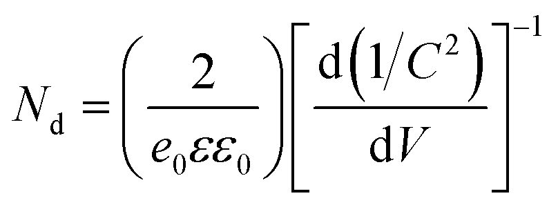
The schematic of the fabricated photodetector using undoped and Sb-doped ZnO NRAs as the photoactive material is shown in Fig. 4(a). The Ag/FTO/ZnO NRA/Ag device was fabricated by the thermal evaporation of a Ag electrode on the hydrothermally grown ZnO NRAs. Ag dots were also deposited on FTO glass to complete the electrical circuit for photodetection. A photograph of the device is shown in Fig. 4(b). The contact between ZnO and the Ag electrode is known as ohmic contact due to the energy positions of the work function and Fermi level of Ag and ZnO, respectively. However, the Ag electrode deposited on the nanorod bundle is too thin, and thus, the pointed Au probe can penetrate the Ag electrode and make direct contact with the ZnO NRs. This partial contact of the Au probe with ZnO induces non-ohmic contact behavior in the I–V curve. Fig. 4(c) compares the electrical conductivity of the undoped and Sb-doped ZnO NRA photodetectors in the dark and under UV irradiation. Two overlapping dark currents are magnified in the inset of Fig. 4(c), and it can be seen that the Sb-doped ZnO NRA device has a higher conductivity than the undoped device in dark conditions. When the NRAs are irritated with UV light, drastic changes in the current generation were observed for both the undoped and Sb-doped ZnO NRAs, as shown in Fig. 4(c). The photoconductivity curve of the Sb-doped ZnO photodetector under UV illumination is limited by the programmed compliance current. Resistance changes of the undoped and Sb-doped ZnO NRAs near 0 V are observed. The resistance of the undoped ZnO photodetector is reduced from 7.03 × 10⁹ (in the dark state) to 1.50 × 10⁴ Ω (under UV irradiation), indicating that the conductivity increases by ∼5 orders of magnitude. The Sb-doped ZnO photodetector shows a more dramatic decrease in the resistance from 7.92 × 10⁸ (in the dark state) to 1.67 × 10² (under UV irradiation), and the conductivity is increased by more than 6 orders of magnitude. Under UV illumination, the conductivity of the ZnO NRA increases by 2 orders of magnitude after Sb doping. The increase in the carrier concentration and oxygen molecule adsorption cause this enhancement, as will be discussed in the mechanism below. This enlarged on-current also indicates the possibility of achieving photodetecting properties at very low applied bias. Mott Schottky analysis is conducted for compare the free-charge-carrier density of each ZnO NRAs directly. A donor density can be calculated with analysing Mott Schottky plot according to the eqn (2):
 | (2) |
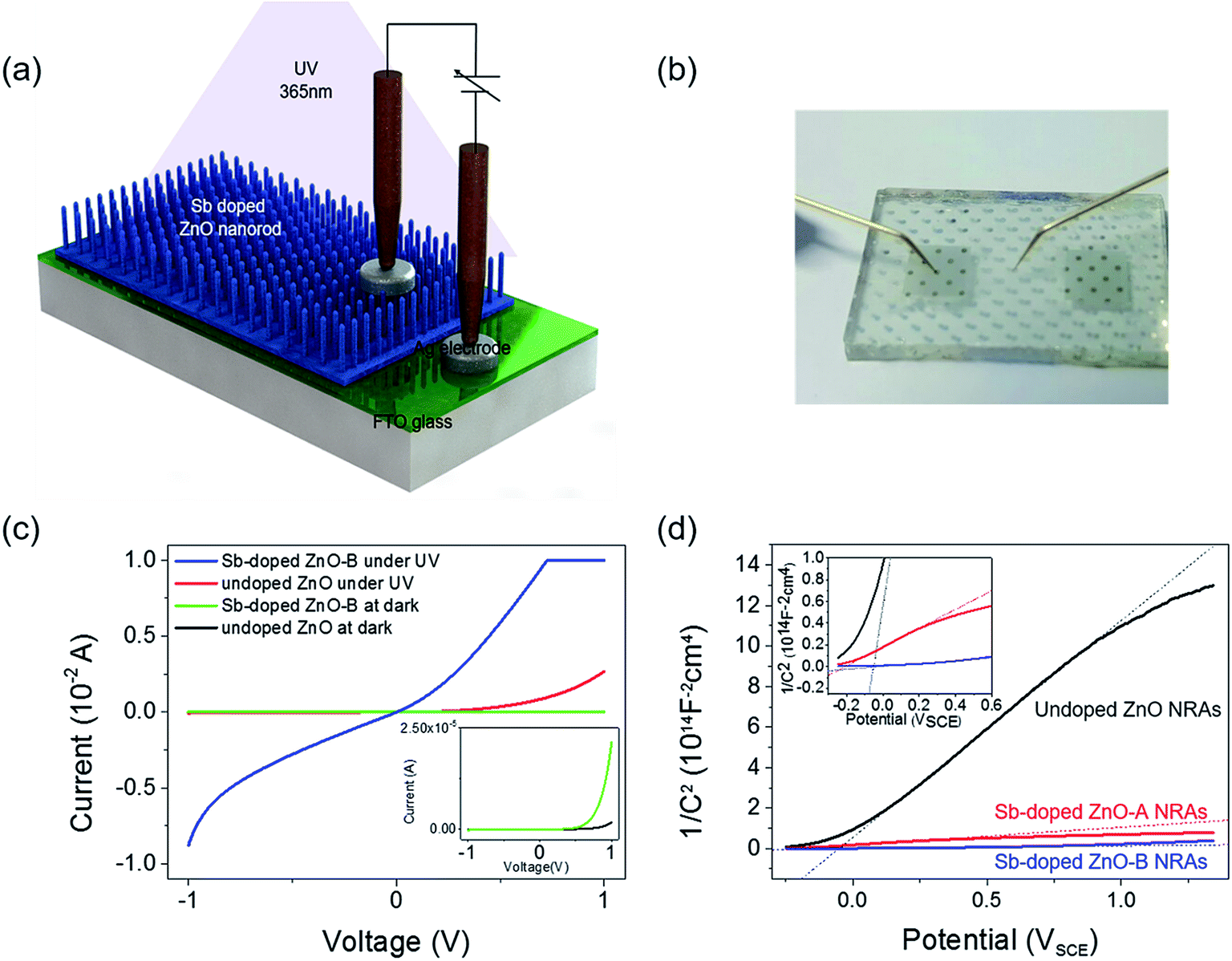 | ||
| Fig. 4 (a) Schematic of the ZnO NRA photodetector. (b) Optical photograph of the ZnO NRA photodetector device. (c) I–V curves of the undoped and Sb-doped ZnO-B NRA photodetector devices measured in the dark and under UV illumination (365 nm). Inset of (c) shows the dark currents of the undoped and Sb-doped ZnO NRA devices. (d) Mott–Schottky plots of undoped ZnO, Sb-doped ZnO-A, Sb-doped ZnO-B collected at a frequency of 10 kHz in dark (inset) magnified image of Mott–Schottky plot of Sb-doped ZnO-A, B NRAs. | ||
The mechanism for the improved photodetecting performance of the Sb-doped ZnO NRAs is proposed, as illustrated in Fig. 5. The conduction channels of the undoped and Sb-doped single ZnO NRs are illustrated in left two part of the Fig. 5, respectively. For the undoped ZnO NR, under vacuum state, naturally generated oxygen vacancies donate electrons, which are distributed over the whole ZnO nanorod and form a conduction channel following a formula: O2− → VO + 2e−. In the Sb-doped ZnO NR, more electrons are generated by the higher concentration of oxygen vacancies, which are formed from the contorted crystal structure due to the large atomic size of Sb. The additional increase in charge carriers occurs due to substitutional-doped Sb atoms donating electrons, as discussed above. Thus, Sb-doped ZnO NRs show a higher conductivity under dark conditions compared to undoped ZnO NRs. When undoped and Sb-doped ZnO NRAs were exposed to ambient air, as shown in middle part of the Fig. 5, oxygen molecules adsorb on the ZnO NRs and extract electrons from ZnO. The electrons bound to the adsorbed oxygen create an electrical depletion layer, which impedes the electric flow and decreases the conductivity. More oxygen molecules absorb on the Sb-doped ZnO NR surface due to the higher electron density compared to the undoped ZnO NRs. In this case, the conductivity decrease is enhanced upon oxygen adsorption because the higher coverage of adsorbed oxygen induces the further formation of the depletion layer. Under UV illumination, electron–hole pairs are generated from excitation of the direct-bandgap ZnO NRs. The generated holes recombine with the electrons bound to oxygen molecules and cause the desorption of oxygen gas from the ZnO NR surface. Upon oxygen desorption, as seen in right part of the Fig. 5, the undoped and Sb-doped ZnO NRs recover their conductivity. More oxygen molecules desorb from the Sb-doped ZnO NRs, causing a greater increase in the conductivity.
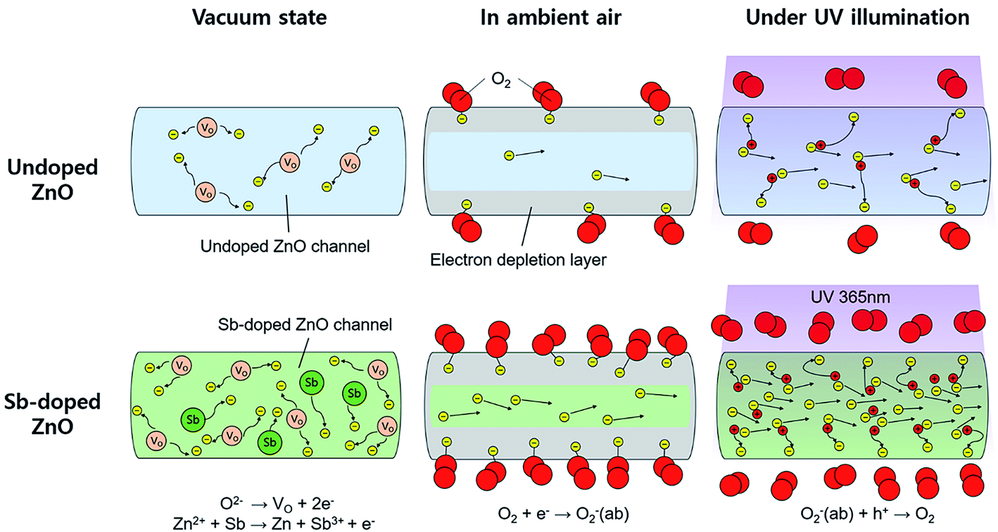 | ||
| Fig. 5 Illustration of the UV-induced photoconductivity mechanism of a single undoped ZnO nanorod (top row) and a single Sb-doped ZnO nanorod (bottom row) at room temperature under vacuum (first column), in ambient air (second column), and under UV illumination (third column). | ||
The reversible switching behaviors of the photodetector devices fabricated using undoped ZnO, Sb-doped ZnO-A, and Sb-doped ZnO-B NRAs were investigated, and the photoconductivity changes are in Fig. 6. The conductivity was measured by turning the UV lamp on and off every 10 minutes with application of a constant voltage of ∼0.5 V. The on-current is drastically increased after Sb doping by ∼5 times for Sb-doped ZnO-A (from 2.41 × 10⁻⁵ to 1.24 × 10⁻⁴ A) and ∼9 times for Sb-doped ZnO-B (from 2.41 × 10⁻⁵ to 2.14 × 10⁻⁴ A) compared with the on-current of undoped ZnO. The electrons increased due to the Sb dopants and increased oxygen vacancies, increasing the conductivity of Sb-doped ZnO under UV illumination. Responsivity, which is the output current divided by total light power, is an important parameter to evaluate sensing properties. The responsivity (R) of the photodetector was calculated using a following eqn (3):
 | (3) |
 | (4) |
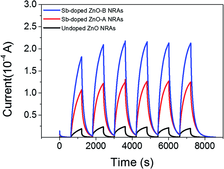 | ||
| Fig. 6 Reversible switching of the undoped ZnO, Sb-doped ZnO-A, and Sb-doped ZnO-B NRAs between the low- and high-conductivity state when the UV lamp was turned on and off. A constant voltage of 0.5 was applied during the measurements. | ||
The highly enhanced photoconductivity of our Sb-doped ZnO NRA photodetector opens the possibility of low-power photodetecting performance. In Fig. 7, the electrical properties of the undoped and Sb-doped ZnO-B NRAs were measured near zero bias. The reversible switching was measured by turning the UV lamp on and off every 10 minutes under a constant applied voltage of 10−6 V (the input voltage on the computer was 0 V, but the source-meter apparatus displayed 10−6 V). The undoped ZnO NRA shows no conductivity response against UV light (black dots in Fig. 7(a)), except for some noise at the moment the light is turned on or off. However, the Sb-doped ZnO-B NRA showed a photoresponse near 10−7 A. The current of the Sb-doped ZnO NRA was enhanced by 2 orders of magnitude under UV light illumination, which clearly shows the UV-induced photoresponse. To analyze the cause of this behavior, the region of the I–V curves near 0 V in Fig. 4(c) is magnified in Fig. 7(b). Unlike the curves corresponding to the dark state or the undoped ZnO NRA, the Sb-doped ZnO NRA under UV light illumination shows high conductivity (slope of the curve) and seems to have short-circuit current and open-circuit voltage (y- and x-intercepts, respectively), similar to solar cell devices. In solar cells, electrons flow through p–n junctions using their band structure difference, without external bias.47 It is speculated that Sb dopants bend the band structure causing Schottky barrier at the interface, which induces current flows.48 This increased electron concentration, and Schottky barrier may facilitate zero-biased UV sensing,22 but the exact principle is hard to define at this stage and needs further study for elucidation. However, our current observation of the almost zero bias detection of UV by the Sb-doped ZnO NRAs is very promising for the development of extremely low-power UV photodetectors. The responsivity is also calculated at zero biased condition to evaluate its sensing property. The responsivity is 0.02, and this value is used to calculate the quantum efficiency (QE) which is the ratio of the number of charge carriers collected by photodetector to the number of photons, using following eqn (5):
 | (5) |
 | ||
| Fig. 7 (a) Zero-biased, reversible switching of the undoped and Sb-doped ZnO-B NRAs between the low- and high-conductivity state when the UV lamp was turned on and off. The input voltage was 0 V on the computer, but the source-meter apparatus displayed 10−6 V. (b) I–V curves near 0 V for the undoped and Sb-doped ZnO-B NRA photodetector devices measured in the dark and under UV illumination (365 nm). | ||
As an additional study, we have tested a modified structured photodetector by deposition of conducting polymer, PEDOT:PSS, on Sb-doped ZnO-B NRAs. The insertion of conducting polymer has recently been introduced in nanorods sensors.42,49,50 Fig. 8 shows a scheme of the device and its reversible switching properties under a constant applied voltage of 10−6 V, which is the same condition as the measurement in Fig. 7(a). The UV lamp was turned on and off every 5 minutes, and the device showed a negative photoresponse near 5 × 10⁻⁸ A, as seen in Fig. 8(c). Unlike the original photodetector showing gradient photocurrent change, the modified device with a semiconductor-conducting polymer junction showed prompt current change. In this photodetector structure, when electron–hole pairs are generated by UV illumination, generated holes from valence band transfer to HOMO (highest occupied molecular orbital) level of PEDOT:PSS layer, which induces photocurrent generation near 0 bias (Fig. 8(b)). It is remarkable that response speed is faster than noise time when UV lamp is turned on. However, the generated photocurrent intensity is decreased by ∼50% compared to the original device, which is plausibly caused by shading effect of light through over-layer of conducting polymer on ZnO NRAs. Similar trends were also found on photodetection of the modified devices under biased conditions.
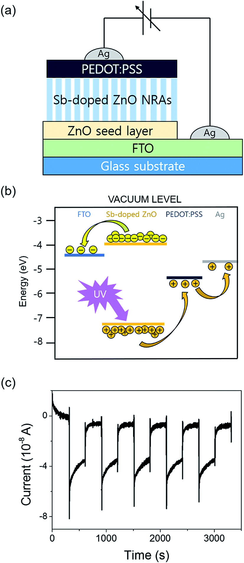 | ||
| Fig. 8 (a) Schematic illustration of Sb-doped ZnO-B NRAs/PEDOT:PSS photodetector device. (b) Schematic illustration of energy band diagram of Sb-doped ZnO-B NRAs/PEDOT:PSS photodetector device. (c) Zero-biased reversible switching of Sb-doped ZnO-B NRAs/PEDOT:PSS. | ||
Conclusion
Sb-Doped ZnO nanorod arrays with high density were easily synthesized by an inexpensive hydrothermal growth method. The nanorod array morphology was confirmed in the SEM images, and their Wurtzite crystal structure was analyzed using HRTEM images, SAED patterns, and XRD measurements. The existence and control of Sb dopants were confirmed by TEM EELS elemental mapping and SIMS analysis. XPS data proved that Sb atoms are substitutionally doped to Zn, forming Sb–O bonds, and oxygen vacancies are increased after doping treatment. Through these analyses, the doped Sb and increased oxygen vacancies were found to provide higher photodetecting activity, because Sb doping induces higher oxygen adsorption coverage on the ZnO NR surface and enlarges the electrical depletion layer in the NRs. In our Ag/FTO/ZnO NRA/Ag photodetecting devices, the photocurrent under UV light illumination was dramatically increased by ∼9 times after Sb doping. The UV sensing properties of ZnO NRAs show stable photodetection with high reversibility and durability. The response and recovery time constants were not greatly affected by Sb doping in the current study. However, the increased electron concentration and partial Schottky contact between the Sb-doped ZnO NRAs, and the electrode show the possible application of the material in extremely low-power photodetectors that activate near 0 V. Unlike undoped ZnO, our Sb-doped ZnO NRAs show a clear photoresponse at 10–6 V with a current that is reversibly increased by 2 orders of magnitude. In addition, photodetector device which has junction with conducting polymer shows improved UV response speed. In summary, our simple hydrothermally grown Sb-doped ZnO NRAs demonstrate greatly improved UV sensing properties in under conditions of general voltage as well as near 0 V bias for application in extremely low-power photodetectors.Conflicts of interest
There are no conflicts to declare.Acknowledgements
This work was supported by the National Research Foundation of Korea (NRF-2016R1A4A1010735).References
- G.-H. Shen, A. R. Tandio and F. C.-N. Hong, Thin Solid Films, 2016, 618, 100–106 CrossRef CAS.
- Y. A. Zhang, L. C. He, T. Jin, T. L. Guo, X. T. Zhou and Z. X. Lin, J. Alloys Compd., 2016, 688, 77–82 CrossRef CAS.
- Y. Xu, T. Liu, Z. Li, B. Feng, S. Li, J. Duan, C. Ye, J. Zhang and H. Wang, Appl. Surf. Sci., 2016, 388, 89–96 CrossRef CAS.
- N. Liu, G. Fang, W. Zeng, H. Zhou, F. Cheng, Q. Zheng, L. Yuan, X. Zou and X. Zhao, ACS Appl. Mater. Interfaces, 2010, 2, 1973–1979 CAS.
- Y. Tak, S. J. Hong, J. S. Lee and K. Yong, J. Mater. Chem., 2009, 19, 5945–5951 RSC.
- J. Kim and K. Yong, J. Phys. Chem. C, 2011, 115, 7218–7224 CAS.
- J. Kim, W. Kim and K. Yong, J. Phys. Chem. C, 2012, 116, 15682–15691 CAS.
- J. Park, H. Song, E. K. Lee, J. H. Oh and K. Yong, J. Electrochem. Soc., 2015, 162, H713–H718 CrossRef CAS.
- S. Lee, J. Lee, J. Park, Y. Choi and K. Yong, Adv. Mater., 2012, 24, 2418–2423 CrossRef CAS PubMed.
- D. Park and K. Yong, J. Vac. Sci. Technol., B: Microelectron. Nanometer Struct.--Process., Meas., Phenom., 2008, 26, 1933–1936 CAS.
- R. Wang, H. Lin, C. Wang and C. Liu, Adv. Funct. Mater., 2012, 22, 3875–3881 CrossRef CAS.
- M. H. Mamat, Z. Khusaimi, M. Z. Musa, M. F. Malek and M. Rusop, Sens. Actuators, A, 2011, 171, 241–247 CrossRef CAS.
- V. Srikant and D. R. Clarke, J. Appl. Phys., 1998, 83, 5447–5451 CrossRef CAS.
- B. K. Meyer, in New Data and Updates for IV-IV, III-V, II-VI and I-VII Compounds, their Mixed Crystals and Diluted Magnetic Semiconductors, Springer, 2011, p. 594 Search PubMed.
- L.-C. Chen, Y.-J. Tu, Y.-S. Wang, R.-S. Kan and C.-M. Huang, J. Photochem. Photobiol., A, 2008, 199, 170–178 CrossRef CAS.
- S. S. Shinde and K. Y. Rajpure, J. Alloys Compd., 2012, 522, 118–122 CrossRef CAS.
- H. S. Al-Salman and M. J. Abdullah, J. Mater. Sci. Technol., 2013, 29, 1139–1145 CAS.
- S. S. Shinde and K. Y. Rajpure, Mater. Res. Bull., 2011, 46, 1734–1737 CrossRef CAS.
- O. Lupan, V. Cretu, V. Postica, M. Ahmadi, B. R. Cuenya, L. Chow, I. Tiginyanu, B. Viana, T. Pauporté and R. Adelung, Sens. Actuators, B, 2016, 223, 893–903 CrossRef CAS.
- O. Lupan, L. Chow, L. Ono, B. Cuemya, G. Chai, H. Khallaf, P. Sanhoon and A. Schulte, J. Phys. Chem. C, 2010, 114, 12401–12408 CAS.
- H. Gong, J. Q. Hu, J. H. Wang, C. H. Ong and F. R. Zhu, Sens. Actuators, B, 2006, 115, 247–251 CrossRef CAS.
- Y. Yang, W. Guo, J. Qi, J. Zhao and Y. Zhang, Appl. Phys. Lett., 2010, 97, 223113 CrossRef.
- X. Fang, J. Li, D. Zhao, B. Li, Z. Zhang, D. Shen, X. Wang and Z. Wei, Thin Solid Films, 2010, 518, 5687–5689 CrossRef CAS.
- T. H. Kao, J. Y. Chen, C. H. Chiu, C. W. Huang and W. W. Wu, Appl. Phys. Lett., 2014, 104, 111909 CrossRef.
- L. M. Li, C. C. Li, J. Zhang, Z. F. Du, B. S. Zou, H. C. Yu, Y. G. Wang and T. H. Wang, Nanotechnology, 2007, 18, 225504 CrossRef.
- C. H. Park, S. B. Zhang and S.-H. Wei, Phys. Rev. B: Condens. Matter Mater. Phys., 2002, 66, 73202 CrossRef.
- D. Kim, I. Yun and H. Kim, Curr. Appl. Phys., 2010, 10, S459–S462 CrossRef.
- J. Hu and R. G. Gordon, Sol. Cells, 1991, 30, 437–450 CrossRef CAS.
- H. J. Ko, Y. F. Chen, S. K. Hong, H. Wenisch, T. Yao and D. C. Look, Appl. Phys. Lett., 2000, 77, 3761–3763 CrossRef CAS.
- F. X. Xiu, Z. Yang, L. J. Mandalapu, J. L. Liu and W. P. Beyermann, Appl. Phys. Lett., 2006, 88, 52106 CrossRef.
- F. X. Xiu, Z. Yang, L. J. Mandalapu, D. T. Zhao, J. L. Liu and W. P. Beyermann, Appl. Phys. Lett., 2005, 87, 152101 CrossRef.
- S. Y. Bae, C. W. Na, J. H. Kang and J. Park, J. Phys. Chem. B, 2005, 109, 2526–2531 CrossRef CAS PubMed.
- P. J. Tsang, R. M. Anderson and S. Cvikevich, J. Electrochem. Soc., 1976, 123, 57–63 CrossRef CAS.
- C. Zhao, S. Feng, R. Xu, C. Shi and J. Ni, Chem. Commun., 1997, 945–946 RSC.
- A. Pfahnl, J. Electrochem. Soc., 1963, 110, 381–384 CrossRef CAS.
- B. Wang, M. J. Callahan, L. O. Bouthillette, C. Xu and M. J. Suscavage, J. Cryst. Growth, 2006, 287, 381–385 CrossRef CAS.
- S. Yun, J. Lee, J. Yang and S. Lim, Phys. B, 2010, 405, 413–419 CrossRef CAS.
- F. Wang, J.-H. Seo, D. Bayerl, J. Shi, H. Mi, Z. Ma, D. Zhao, Y. Shuai, W. Zhou and X. Wang, Nanotechnology, 2011, 22, 225602 CrossRef PubMed.
- H. Wang, S. Baek, J. Song, J. Lee and S. Lim, Nanotechnology, 2008, 19, 75607 CrossRef PubMed.
- M. H. Mamat, M. Z. Sahdan, Z. Khusaimi, A. Z. Ahmed, S. Abdullah and M. Rusop, Opt. Mater., 2010, 32, 696–699 CrossRef CAS.
- Y. Tak and K. Yong, J. Phys. Chem. B, 2005, 109, 19263–19269 CrossRef CAS PubMed.
- B. D. Boruah, S. N. Majji and A. Misra, Nanoscale, 2017, 9, 4536–4543 RSC.
- A. Ghobadi, T. G. Ulusoy, R. Garifullin, M. O. Guler and A. K. Okyay, Sci. Rep., 2016, 6, 30587 CrossRef CAS PubMed.
- M. Baek, D. Kim and K. Yong, ACS Appl. Mater. Interfaces, 2017, 9, 2317–2325 CAS.
- S. Hullavarad, N. Hullavarad, D. Look and B. Claflin, Nanoscale Res. Lett., 2009, 4, 1421 CrossRef CAS PubMed.
- C. F. Windisch Jr and G. J. Exarhos, J. Vac. Sci. Technol., A, 2000, 18, 1677–1680 Search PubMed.
- V. H. T. Pham, N. T. N. Truong, T. K. Trinh, S. H. Lee and C. Park, Korean J. Chem. Eng., 2016, 33, 678–682 CrossRef CAS.
- X. Li, H. Zhu, K. Wang, A. Cao, J. Wei, C. Li, Y. Jia, Z. Li, X. Li and D. Wu, Adv. Mater., 2010, 22, 2743–2748 CrossRef CAS PubMed.
- F. Yi, Q. Liao, Y. Huang, Y. Gu and Y. Zhang, Semicond. Sci. Technol., 2013, 28, 105023 CrossRef.
- A. E. Rakhshani, Appl. Surf. Sci., 2014, 311, 614–620 CrossRef CAS.
Footnote |
| † Electronic supplementary information (ESI) available. See DOI: 10.1039/c7ra07157d |
| This journal is © The Royal Society of Chemistry 2017 |