
 Open Access Article
 This Open Access Article is licensed under a
 Creative Commons Attribution 3.0 Unported Licence
Self-formed nanogap junctions for electronic detection and characterization of molecules and quantum dots†
Amir Ziv a,
Avra Tzaguyb,
Ori Hazutb,
Shira Yochelisa,
Roie Yerushalmi*b and
Yossi Paltiel*a
a,
Avra Tzaguyb,
Ori Hazutb,
Shira Yochelisa,
Roie Yerushalmi*b and
Yossi Paltiel*a
aDepartment of Applied Physics, The Hebrew University of Jerusalem, 9190401 Israel. E-mail: paltiel@mail.huji.ac.il
bInstitute of Chemistry, The Center for Nanoscience and Nanotechnology, The Hebrew University of Jerusalem, Edmond J. Safra Campus, Givat Ram, Jerusalem, 9190401, Israel. E-mail: roie.yerushalmi@mail.huji.ac.il
First published on 15th May 2017
Abstract
Fabrication of self-forming nanojunction devices is demonstrated using positioning of nanofloret-like building blocks that serve as self-assembled electrodes. A main feature of the device is a self-formed nanogap bridging between the nanofloret (NF) hybrid nanostructures (HNS) and a macroscopic counter-electrode. When nanostructures are introduced to the device they provide facile bridging across the nanostructure. This strategy is used to demonstrate electronic measurements across molecules and nanoparticles. Connecting the NF nanojunction to the micro-, and macro-scales is achieved by applying standard, robust, optical lithography. In addition, the devices are operable at ambient conditions and in solvent environments, where introducing molecules to the device results in a prominent change in the conductance characteristics. Furthermore, introduction of quantum dots results in the mapping of their band structure at ambient conditions. Our results provide a proof-of-concept of large scale self-forming nanogap device platform realized using simple fabrication tools. Such a technology can be used for molecular detectors, as a potential building block for molecular electronics, or as a platform for fundamental research.
Introduction
Coupling standard electronic circuits with large size contacts to the nanoscale molecular-level and nanoparticles is an attractive concept with intense research and technological activity.1–5 Central to this concept is the transport of charge carriers through a single molecule, or a small ensemble of molecules. Transport properties in molecules exploit the richness, versatility, repeatability and functionality that are the hallmarks of molecular components in the context of electronic devices.1 Current synthesis methods offer a large variety of molecules and nanoscale building blocks with high purity, tunable electronic structure, connectivity and functionalities, together with uniform size and composition. This makes them attractive candidates for integration as electronic components. However, despite these advances, substantial obstacles are still present when coupling molecular and nanoscale building blocks to external electrodes, which hamper the exploitation of their huge potential for large scale electronic components. These difficulties are both technical and fundamental in nature. One technical challenge is the fabrication of contacts to the element under study, such as a molecule, or a quantum dot, without causing damage or altering its electronic properties. Two of the key fundamental issues are (i) keeping the connection stable for long time periods, and (ii) controlling the chemical or physical bonding between the element under study and the electrodes.6 A promising approach for overcoming some of these obstacles involves nanogap architectures with good conductivity to the respective element under study, which is also commonly termed registry. Fabricating nanogap devices with specific dimensions is not simple and usually requires complicated technology, making the fabrication yield of two-terminal connectivity nanogap junctions quite low. Indeed, significant efforts have been dedicated toward the realization and study of nanogap architectures for diverse applications including molecular rectifiers, switching and electro-chemical sensors.7–9 These efforts yielded great advances in the study of the transport properties of molecular junctions in two-terminal devices, serving as a powerful platform for research at the single-molecule level. Similar studies were conducted using STM/AFM-based junctions,10 mechanically-controlled break junctions11 and electromigration-controlled gaps.12 While all these platforms yielded fundamental insights and research tools for charge and energy transport for single molecules,13 the fabrication methods are usually complex and require advanced e-beam lithography, high-vacuum conditions, or complicated feedback mechanisms for junction formation.These methods inhibit the realization and integration of these classes of devices. Fabricating small and compact junctions usually requires complex, multi-step processes which are not easily reproducible or scalable, and are not compatible with standard clean room methods.12,14 On the other-hand, simple methods for fabricating nanogaps, usually have low control over gap size15 or are limited in scaling the junction cross section.16,17 Therefore, it is highly desired to develop nanogap device fabrication schemes that would be compatible with standard silicon device technologies. Such hybrid integrated circuits have the potential to be operated, tested, and to function under ambient conditions and may open the way for utilization of such devices in numerous applications.
Here, we present a fabrication method for a self-formed nanojunction based on nanofloret (NF) hybrid nanostructures (HNS) using SiGe nanowires (NWs) grown at selective locations. The fabrication process is robust, using simple lithographic methods (top-down) for the micron-scale parts of the device, and bottom-up methods for the nanoscale elements. The nanogap is self-formed, created by wet processing at ambient conditions, whereas the gap size is adjustable according to the trapped nanostructure. High geometrical aspect ratio SiGe NWs are used to form the nanofloret HNS where a metallic nanoshell cap that function as a contact is deposited selectively at the NW tip.18 The length of the NWs can be tuned between 1–10 microns, enabling to bridge the gap between two distant optical lithography fabricated contacts. The active junction is formed between the edge of the NF where the metallic cap is deposited by wet process and the counter electrode with a very small contact area owing to the geometry of the NF HNS. I–V transport measurements performed after the introduction of molecules and quantum dots (QD) into the system reveal that they control and change the junction conductance, thus establishing a simple molecular detector and provides information on their electronic structures. The resulting platform is a first step towards achieving a simple and robust method to study and control of molecular- and nanostructure-based electronic devices.
Results and discussion
Typical fabrication of self-forming nanogap junction device includes the following process steps, depicted in Fig. 1a: (I) gold nanoparticles are selectively adsorbed at the edge of one of the two prefabricated Ti contacts separated by a micrometric gap. (II) The sample is inserted into a Chemical Vapor Deposition (CVD) system, where SiGe nanowires are grown where the gold nanoparticles act as growth catalysts, similar to related works.19–22 | ||
| Fig. 1 NF-based nanogap electronic junction. (a) Summary of the fabrication process: first, fabrication of micro-scale metal electrodes using simple photolithography, followed by selective adsorption of gold nanoparticles on one of the electrodes that will act as catalysts for the CVD growth of the NWs. Then, insertion of the sample into a CVD system, where SiGe NWs are grown, to eventually lay horizontally to form the nanojunction. Lastly, synthesis of the NFs. (b) Optical image of a NF junction array, where the black lines correspond to locations where NFs were selectively grown. Inset: scanning electron microscope image of the nanojunction, where several NFs are shown bridging the gap between the two metal electrodes. (c) The NF junction facilitates the bridging from the nanoscale and sub-nanoscale to the macro scale. | ||
The length of the NWs is controlled by the CVD growth parameters and deposition time and the density and position of NWs seeds is controlled by the selective adsorption of nanoparticles. (III) Above several μm in length, the NWs do not stand vertically but rather fall and lay horizontally, where the ones at the edge of the contact tends to fall outwards, thus bridging the gap between the contacts. (IV) NF HNS are synthesized as described previously,18 the wetting and drying of the samples during the NF synthesis results in collapse of the high aspect ratio HNS onto the device substrate because of capillary forces, increasing the probability of nanojunction formation.
Notably, this procedure requires simple and crude lithographic techniques and wet chemical methods, while no electrical or mechanical forces have been applied in order to align the NFs, unlike other alignment methods.23–25 In addition, the resulting nanojunction device is compact, requires no feedback system and is stable under ambient conditions, which makes it suitable for integration in complex measurement systems. The junction by itself is stable in various chemical and biological conditions, thus enabling measurements at variant conditions.
The inset of Fig. 1b presents an example (SEM image) of a NF-based junction device. Here, several NFs are shown bridging a micrometric gap between two metal electrodes, thus allowing current to flow when a voltage is applied across the contacts. The size of the established nanojunction depends on the contact area between the NF tip and the counter electrode, whereas in the investigated devices described here, the junction is typically ∼60 nm in length. The junction size can be altered as the NF dimensions can be controlled.18 An optical microscope image of the fabricated junctions is shown in Fig. 1b. The black lines identify the selective area where the NF is grown. Current can only flow through the NF and not through the substrate due to the 1 [μm] SiO2 insulating layer on top of the substrate. Note that typically several junctions are formed. Therefore, the measurements consist of multiple nanogap junctions per device. The NF density can be varied for attaining many- or few-nanogap junction devices and by that control the device sensitivity.
Ti metal contacts bridged by the NF HNS were deposited for compatibility with the CVD process and subsequent chemical processing. These contacts were used as they form a good ohmic contact with the SiGe NF. At the tip of the NF a metal-semiconductor junction is created between the semiconducting NW and the gold nanoshell, forming a Schottky junction. The NF length is determined by the duration of growth in the CVD system and can be adjusted to match or exceed the size of the gap between electrodes. Over-growth of the NWs used for NF synthesis offers additional flexibility in the fabrication process. NF HNS length can be tuned such that the contact is formed at the counter electrode either with the gold shell at the tip only, or by the semiconducting NW as well. The electronic behavior in the two cases is clearly different as shown in Fig. 2. When the contact between the counter electrode and the NF is limited to the gold shell at tip, a diode-like behavior is obtained and the nature of the junction is that of a Schottky junction. In contrast, when the semiconducting NW bridges both sides of the junction, an ohmic contact is formed on both sides and the behavior is more symmetric. These results are in-line with previously performed measurements on similar Schottky junctions on Ge NWs.26 Moreover, these results demonstrate the significant influence of the gold nanoshell cap on the electronic behavior of the hybrid nanostructure, which is an important feature when introducing molecules to the system at the interface of the NF shell and counter electrode.
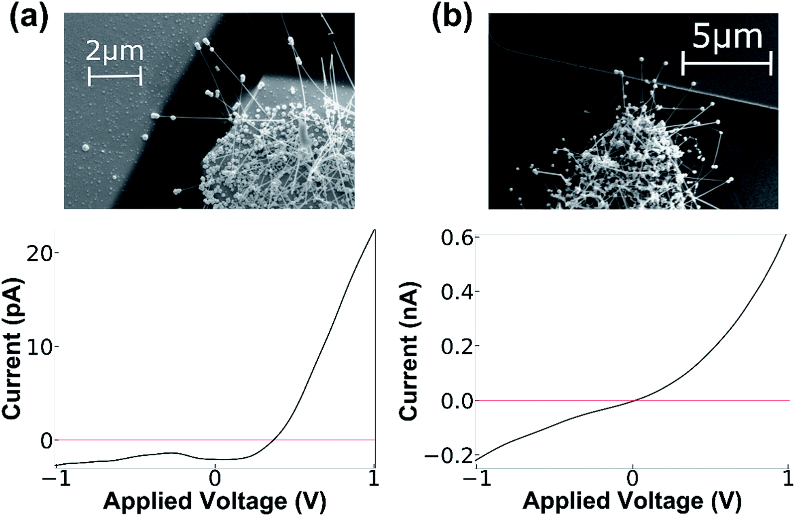 | ||
| Fig. 2 Current vs. voltage measurements of NF junctions. (a) A junction measurement where only the gold nanoshell of the NF bridges the junction. This results in a rectifying behavior due to the Schottky junction between the gold and the semiconductor. (b) Both NW facet and tip contact is achieved when the NF is allowed to grow in such a way that not only the gold nanoshell touches the counter electrode but also the NW facets bridge the junction. | ||
The electronic response of the NF junction resulting from adsorption of molecules was studied on junctions of the second type, i.e., junctions where both the gold cap and the semiconducting NW are touching the counter electrode (Fig. 2b). This was achieved by performing a sequence of three consecutive experiments for each device in an inert environment. The measurements were performed at three stages: the first measurement was taken before any chemical treatment, the second after 20 microliters of absolute ethanol was dripped onto the sample and allowed to dry, and the third measurement was performed after dripping 20 microliters of 5 mM ethanol solution of cysteamine.
This allowed us to identify conductance changes that might arise from the introduction of solvent apart from those related to molecular adsorption at the junction, possibly arising from mechanical changes induced, for example, by capillary forces that the solvent treatment may cause. This procedure allowed us to exclude the contribution of such effects demonstrated by two distinct examples of typical measurements in Fig. 3. In both cases, only minor differences are present between the measurement before and after ethanol treatment, however dripping the cysteamine solution resulted in a large decrease in conductance. By inspecting the numerical derivative (dI/dV) of the first example (Fig. 3a and b) one notices a big energy gap. When molecules are captured a nanogap is formed changing the conductivity. In (Fig. 3c and d), the numerical derivative (dI/dV) shows that the conductance was reduced, but with no clear energy gap. These results demonstrate two cases: (1) molecules intercalate at the interface between the NF and the Ti electrode resulting in electron transport through the adsorbed molecules (see Fig. 3a and b), and (2), a change in conductance due to the presence of molecules on the surface of the semiconducting NW, which has altered the band bending and thus changed the electron density27,28 (see Fig. 3c and d). The interplay and control of the two transport mechanisms, through the SC NW surface in contact with the electrode and directly through the NF gold cap is under further study and optimization. The adsorption of molecules was further verified by XPS measurement and gold nanoparticle adsorption experiments (see ESI†). All experiments were repeated several times with several batches of NF nanogap devices to ensure the generality of the results. It is important to note that a small change in the conductance after dripping only the solvent (ethanol) was observed, however, in these cases the change was random and of a smaller magnitude; i.e. in some cases the conductance was improved while in others it was reduced (with an almost equal distribution between the cases – see ESI for more information†). When the cysteamine molecule was introduced to the junction, the conductance was reduced in 70% of the cases. Therefore, we expect that the solvent mechanically changed the position of the NF, while the molecules actually changed the electronic properties of the junction. The generality of the NF-based nanogap devices was further demonstrated by introducing quantum dots (QDs) into the device. This fourth stage was added to the transport measurement sequence, i.e. on the same device, QD were introduced after molecules adsorption. Typical results are shown in Fig. 4, where, similar to the previous cases, introduction of molecules resulted in the characteristics energy gap shown by the numerical derivative (dI/dV). Furthermore, the followed introduction of 2.5 nm CdSe QDs resulted in clear changes of the numerical derivative features, hence the energy gap was reduced and shifted, and new peaks are clearly observed at higher bias voltages (Fig. 4b). We attribute these features to tunnelling through the QD, either between the Ti contact and the gold tip or the semiconducting NW and Ti contact, so that the peaks in the (dI/dV) curve correspond roughly to the energy levels of the QD, considering that our measurements are performed under ambient conditions and not under UHV.29 The 2–2.2 V gap at around zero current is in agreement with the CdSe band gap, though this band gap is smaller than the measured photoluminescence gap of 2.35–2.45 eV (see ESI†).30 This difference is ascribed to the existence of multiple conduction channels available in the NF junction structure. We also note the appearance of negative differential conductance at the regions ±1.5 V, which supports a current flowing in parallel routes.29,31
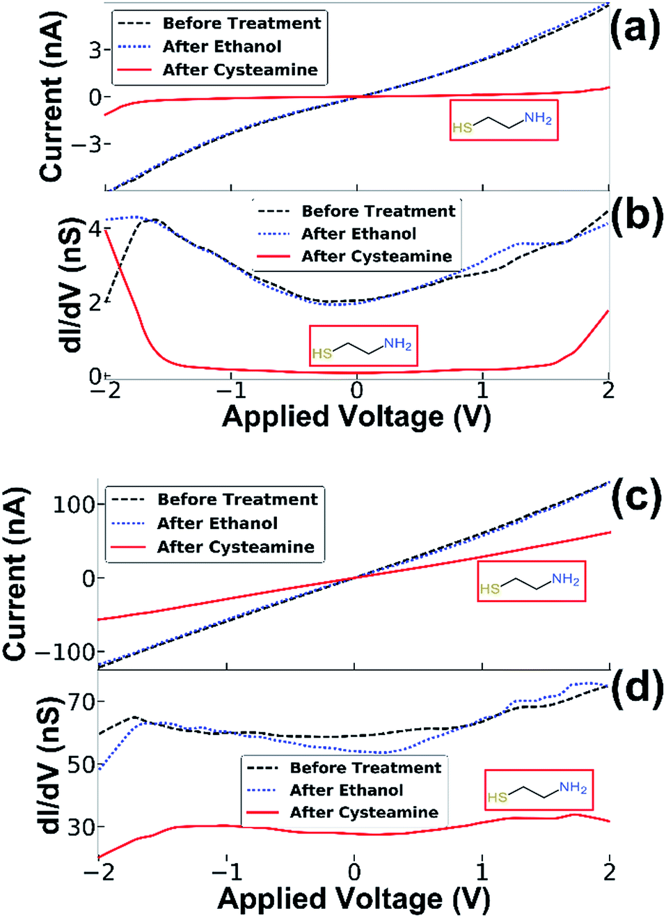 | ||
| Fig. 3 Transport measurements of NF junctions. (a) Current vs. voltage characteristic and (b) its numerical derivative. The formation of an energy gap after the introduction of cysteamine molecules indicates that the electron transport occurs through the molecules. (c and d) Here, the presence of the cysteamine molecules caused a decrease in the conductance, with no energy gap. This indicates that the molecules only affect the conductance of the junction through their adsorption on the NF surface. | ||
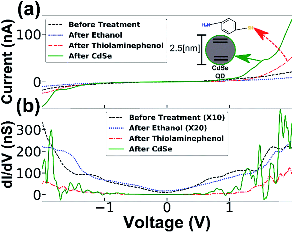 | ||
| Fig. 4 I–V curve of a NF junction device (a) and its numerical derivative (b). Only after the introduction of molecules into the system was a band gap formed, and after the insertion of CdSe QD new peaks appeared, corresponding to the QD energy levels. | ||
Similar experiments were performed by applying the chemical treatment to NWs instead of NF-devices, namely, by repeating exactly the same fabrication procedure but excluding the step where NWs are processed to NF. These experiments with conventional NWs showed no formation of an energy gap. This result further supports the role of the gold nanoshell cap which is unique to the NF architecture and its key role in the trapping of molecules and QDs between the NF and the Ti contact due to the strong covalent bonds between the thiol linkers and the gold tip and its unique geometrical arrangement.
Methods
Electrodes preparation
Si substrates with 1 μm SiO2 layer (University Wafer©) were baked at 120 °C for 5 min to dry them. Then, they were spin-coated with LOR5b for 3 s at 600 rpm, and then for 30 s at 4000 rpm. Afterwards, the samples were baked for 5 min at 200 °C. The samples were then spin-coated with nL of 2020 photoresist for 2 s at 600 rpm and then 40 s at 4000 rpm, followed by a bake for 75 s at 110 °C. The samples were exposed to UV light using a SUSS© MA06 mask aligner for 1.6 s, followed by post-bake of 75 s at 110 °C. Then, the samples were placed in an AZ-726 for 30 s for development. Afterwards, Ti was evaporated at −5 °C at 1 Å s−1 followed by lift-off using N-methyl-2-pyrrolidone (NMP) warmed to 80 °C, 30 s sonication, and rinse with isopropanol and water.Gold nanoparticle selective adsorption
The substrates with the prefabricated contacts were baked at 120 °C for 5 min to dry them. After drying, they were spin-coated with nL of 2020 photoresist for 2 s at 600 rpm and then 40 s at 4000 rpm, followed by baking for 75 s at 110 °C. Gold nanoparticles (30 nm) functionalized covalently with phosphonic acid (Nanopartz™), were dripped onto the samples (∼20 μL, until full coverage) and left on for 30 min. Then, the samples were washed gently in water and dried, followed by 5 min in acetone (“lift off”). Lastly, the sample was rinsed gently again in water and dried.Synthesis of silicon–germanium (Si–Ge) alloy nanowire (NW)
The substrates patterned with Au NPs at specific locations were transferred to a custom-built CVD system, where SiGe NWs with an alloy composition of 1![[thin space (1/6-em)]](https://www.rsc.org/images/entities/char_2009.gif) :18 (Si:Ge) were obtained by flowing 0.5 SCCM of SiH4 and 90 SCCM of GeH4 (10% in H2) for 5 min at 247 °C and 45 Torr.
:18 (Si:Ge) were obtained by flowing 0.5 SCCM of SiH4 and 90 SCCM of GeH4 (10% in H2) for 5 min at 247 °C and 45 Torr.
SiGe nanofloret (NF) synthesis
SiGe alloy NWs that were prepared by CVD on the patterned substrates were stored in an ambient atmosphere for 48 h to form a native oxide layer. Then, Au-NFs were prepared by immersing the substrates with SiGe NWs in an EtOH solution (99%, ACROS Organics) containing 1 mM AuCl3 (99%, ACROS Organics) and 30 μL per mL DI water for 3 min at room temperature, followed by: cleaning in anhydrous ETOH twice, DI water, ETOH again, and drying under a gentle stream of N2. Samples were placed under vacuum for 3 h to remove moisture residues.Electron transport measurements
The prepared samples with the NF junction were bonded using a wire bonder. All electronic measurements were performed inside a sealed chamber (Faraday cage) under constant nitrogen flow. The device was connected via BNC feedthroughs to a Keithley© 6487 Picoammeter/Voltage Source. The voltage sweep was performed in such a way that the current under each voltage was measured 5 times and then averaged. This method results in a noise reduction of the signal.Molecules and QD solutions perpetration
5 mM ethanol solution of cysteamine (Sigma Aldrich©) and 5 mM ethanol solution of thiolaminephenol (Sigma Aldrich©) were prepared for the self-assembly procedure. The QDs that were used are Lumidot™ core-type CdSe 520 [nm] 5 mg mL−1. The QDs solution was diluted 1:20 with anhydrous toluene.
Conclusions
A fast and simple method for the fabrication of nanometer-scale gap devices is presented using nanofloret hybrid nanostructures as building blocks with unique structural characteristics. The nanogap junction devices are used to enable electronic measurements by connecting molecules and QDs to a macroscopic electronic circuit. The unique hybrid metal-semiconductor structure of the modified NWs, nanoflorets, facilitates the intercalation of molecules and nanostructures onto the interfaces formed between the NF and the counter-metal contact, which is exhibited in the characteristics of the electronic measurements and allows qualitative mapping of the semiconducting nanoparticle band structure at ambient conditions. This work establishes a first proof of concept for our platform. The new class of devices presented here were realized using relatively simple fabrication and operation procedures. These devices are attractive for exploiting the vast knowledge gained with platforms such as break junctions in a scalable platform. For applications, such devices are important in a broad context and in a variety disciplines including fundamental research of charge transport through molecules and nanostructures, sensing applications, and more.Acknowledgements
Funding was made possible by Yissum Research Development Company of the Hebrew University of Jerusalem Ltd (“Yissum”)References
- A. Aviram and M. A. Ratner, Chem. Phys. Lett., 1974, 29, 277–283 CrossRef CAS.
- M. Parodi, B. Bianco and A. Chiabrera, Cell Biophys., 1985, 7, 215–235 CrossRef CAS PubMed.
- M. A. Reed, C. Zhou, C. J. Muller, T. P. Burgin and J. M. Tour, Science, 1997, 278, 252–254 CrossRef CAS.
- C. Joachim, J. K. Gimzewski and A. Aviram, Nature, 2000, 408, 541–548 CrossRef CAS PubMed.
- F. S. Kim, G. Ren and S. A. Jenekhe, Chem. Mater., 2011, 23, 682–732 CrossRef CAS.
- H. Häkkinen, Nat. Chem., 2012, 4, 443–455 CrossRef PubMed.
- N. A. Zimbovskaya, Transport Properties of Molecular Junctions, Springer, 2013, pp. 28–33 Search PubMed.
- X. Chen, Z. Guo, G.-M. Yang, J. Li, M.-Q. Li, J.-H. Liu and X.-J. Huang, Mater. Today, 2010, 13, 28–41 CrossRef CAS.
- F. Moresco, Phys. Rev. Lett., 2001, 86, 672–675 CrossRef CAS PubMed.
- B. Xu and N. J. Tao, Science, 2003, 301, 1221–1223 CrossRef CAS PubMed.
- R. H. M. Smit, Y. Noat, C. Untiedt, N. D. Lang, M. C. van Hemert and J. M. van Ruitenbeek, Nature, 2002, 419, 906–909 CrossRef CAS PubMed.
- H. Park, A. K. L. Lim, A. P. Alivisatos, J. Park and P. L. McEuen, Appl. Phys. Lett., 1999, 75, 301–303 CrossRef CAS.
- S. V. Aradhya and L. Venkataraman, Nat. Nanotechnol., 2013, 8, 399–410 CrossRef CAS PubMed.
- A. Guttman, D. Mahalu, J. Sperling, E. Cohen-Hoshen and I. Bar-Joseph, Appl. Phys. Lett., 2011, 99, 063113 CrossRef.
- B. Lam, W. Zhou, S. O. Kelley and E. H. Sargent, Nat. Commun., 2015, 6, 6940 CrossRef CAS PubMed.
- J. Tang, E. P. De Poortere, J. E. Klare, C. Nuckolls and S. J. Wind, Microelectron. Eng., 2006, 83, 1706–1709 CrossRef CAS.
- F. Prins, M. Buscema, J. S. Seldenthuis, S. Etaki, G. Buchs, M. Barkelid, V. Zwiller, Y. Gao, A. J. Houtepen, L. D. A. Siebbeles and H. S. J. van der Zant, Nano Lett., 2012, 12, 5740–5743 CrossRef CAS PubMed.
- O. Hazut, S. Waichman, T. Subramani, D. Sarkar, S. Dash, T. Roncal-Herrero, R. Kröger and R. Yerushalmi, J. Am. Chem. Soc., 2016, 138, 4079–4086 CrossRef CAS PubMed.
- S. Fan, M. G. Chapline, N. R. Franklin, T. W. Tombler, A. M. Cassell and H. Dai, Science, 1999, 283, 512–514 CrossRef CAS PubMed.
- T. Jain, F. Westerlund, E. Johnson, K. Moth-Poulsen and T. Bjørnholm, ACS Nano, 2009, 3, 828–834 CrossRef CAS PubMed.
- T. Jain, S. Lara-Avila, Y.-V. Kervennic, K. Moth-Poulsen, K. Nørgaard, S. Kubatkin and T. Bjørnholm, ACS Nano, 2012, 6, 3861–3867 CrossRef CAS PubMed.
- M. Schvartzman, D. Tsivion, D. Mahalu, O. Raslin and E. Joselevich, Proc. Natl. Acad. Sci. U. S. A., 2013, 110, 15195–15200 CrossRef CAS PubMed.
- J. Yao, H. Yan and C. M. Lieber, Nat. Nanotechnol., 2013, 8, 329–335 CrossRef CAS PubMed.
- A. Pevzner, Y. Engel, R. Elnathan, T. Ducobni, M. Ben-Ishai, K. Reddy, N. Shpaisman, A. Tsukernik, M. Oksman and F. Patolsky, Nano Lett., 2010, 10, 1202–1208 CrossRef CAS PubMed.
- E. M. Freer, O. Grachev, X. Duan, S. Martin and D. P. Stumbo, Nat. Nanotechnol., 2010, 5, 525–530 CrossRef CAS PubMed.
- F. Léonard, A. A. Talin, B. S. Swartzentruber and S. T. Picraux, Phys. Rev. Lett., 2009, 102, 106805 CrossRef PubMed.
- Y. Cui, Q. Wei, H. Park and C. M. Lieber, Science, 2001, 293, 1289–1292 CrossRef CAS PubMed.
- Z. Zhang and J. T. Yates, Chem. Rev., 2012, 112, 5520–5551 CrossRef CAS PubMed.
- S. Vortman, O. Ben-dor, S. Yochelis, Y. Amit and Y. Paltiel, J. Phys. Chem. C, 2013, 117, 22245–22249 CAS.
- L. Jdira, P. Liljeroth, E. Stoffels, D. Vanmaekelbergh and S. Speller, Phys. Rev. B: Condens. Matter Mater. Phys., 2006, 73, 115305 CrossRef.
- R. Pozner, E. Lifshitz and U. Peskin, J. Phys. Chem. Lett., 2015, 6, 1521–1528 CrossRef CAS PubMed.
Footnote |
| † Electronic supplementary information (ESI) available. See DOI: 10.1039/c7ra04600f |
| This journal is © The Royal Society of Chemistry 2017 |