
 Open Access Article
 This Open Access Article is licensed under a Creative Commons Attribution-Non Commercial 3.0 Unported Licence
Luminescence emission-modulated based on specific two-photon compound of triazole-conjugated pyrene derivative†
Huiying Liu a,
Lei Wangb,
Yishi Wu*b and
Qing Liao*c
a,
Lei Wangb,
Yishi Wu*b and
Qing Liao*c
aSchool of Materials Science and Engineering, Beijing Institute of Fashion Technology, Beijing 100029, P. R. China. E-mail: liuhuiying@iccas.ac.cn
bBeijing National Laboratory for Molecular Science (BNLMS), Institute of Chemistry, Chinese Academy of Sciences, Beijing 100190, P. R. China
cBeijing Key Laboratory for Optical Materials and Photonic Devices, Department of Chemistry, Capital Normal University, Beijing, 100048, P. R. China
First published on 30th March 2017
Abstract
A triazole-conjugated pyrene derivative (DTP) with strong two-photon absorption has been synthesized via CuAAC reaction. It can readily self-assemble into ultra-long 1D single-crystal nanowires by a one-step anti-solvent diffusion method, which exhibit exceptional two photon optical waveguides with low optical loss during light propagation. Single-particle spectroscopy of the nanowires clarifies that one short wavelength emission band results from the DTP monomer and the other longer wavelength band is responsible for the aggregate state of DTP. Moreover, DTP monomer and aggregate state emission peaks intensity of a single nanowire have opposite trends by changing the polarization of the incident light, owning to the two orthogonal optical transition dipoles. Besides, the excitation wavelength was changing from 760 nm to 850 nm, resulting in a red-shift of the maximum emission peak from 466 to 522 nm and the variation of the CIE coordinates from blue to green. This result may open up new perspectives in optoelectronic devices.
Introduction
Organic micro/nanostructures with desired sizes and ordered packing have drawn much attention due to their promising applications such as organic solid-state lasers (OSSLs),1–3 sensors,4–6 photodetectors,7 organic light-emitting diodes (OLED),8 optical waveguides,9 organic field-effect transistors (OFET).10–13 Among them, organic single-crystalline nanowires can be used as fundamental elements in optical circuits, which are capable of propagating14 and manipulating light efficiently for potential applications in miniaturized optical devices. In contrast with their inorganic and polymer counterparts, organic nanowires show excellent luminescent properties and can be easily prepared with desired sizes ranging from hundreds of nanometers to several microns.15 However, most of those optical waveguides are one-photon driving systems, which need high excitation energy to stimulate the gain mediums.In recent years, organic conjugated materials with high fluorescence quantum yield and large two-photon absorption (TPA) across section have attracted extensive interests because of their potential wide-ranging applications such as optical power limiting,16 up-converted lasing,17 3D optical data storage,18 and microfabrication,19 bioimaging,20,21 and photodynamic therapy.22 TPA is a process which involves simultaneous two photons of half the energy (or twice the wavelength) to a given excited state of the corresponding one-photon transition absorption. TPA materials usually has broad two-photon excitation window, even extend to the near IR region which is near-transparency window of many biological tissues (700–1000 nm). Thus wavelength of the light for two photon excitation can penetrate deeper into the target with reduced photo-damage to the undesired tissues and meanwhile avoid auto-fluorescence from the biological background.
With the increasing applications, the demands for novel TPA materials become highly urgent. Many efforts have been devoted to the investigation of strong two photon absorption compounds with chromophoric systems (π-center for high luminescent materials) ranging from the well-known oligo(phenylene vinylene)s (OPVs),23 perylene diimide (PDI) derivatives24 to π-extended pyrene derivatives.25 Note that π-extended pyrene derivatives is not only planar configuration but also has emitted significantly red-shifted fluorescence with enhanced quantum yield compared to the parent pyrene fluorophore by introducing appropriate structural modification.26 Meanwhile, π-extended pyrene derivatives usually exhibit strong two-photon absorption cross-section and the incorporation of triazole moieties is an interesting route to tailor the optical properties by coordinated with metal ion.27
Most of the reported TPA materials are focused on enhancing the TPA cross-section in solution, recently a few groups clarified that aggregate will enlarge the cross-section of the TPA.20 However, the spectroscopic emission shape between these solution and their aggregates looks no discrepancy. It is of great scientific interest and technological to tune the fluorescence colour of organic molecules in the solid states for multi-color displays and future light-emitting materials. Herein, we have designed and synthesized a new triazole-conjugated pyrene derivative, 1,6-di(1-butyl-1H-1,2,3-triazol-4-yl)pyrene (DTP) with high quantum yield in two photon excitation fluorescence. It can readily self-assemble into ultra-long 1D single-crystal nanowires by a one-step anti-solvent diffusion method, with the preferential growth along the crystal [100] direction. These DTP nanowires exhibit exceptional two-photon optical waveguides with a propagation loss of 0.0217 dB μm−1. In particular, not only the aggregate state of DTP but also DTP monomer emission was observed in the spatially resolved PL spectra of the nanowires, which is a rare phenomenon in the two photon excitation fluorescence in solid state. The polarization experiment suggests that the orthogonal optical transition dipoles between DTP monomer and DTP aggregate were responsible for the abnormal behaviour. Therefore, we can take advantage of orthogonal optical transition dipoles to modulate the fluorescence emission color by changing excitation wavelength.
Experimental
The DTP nanowires were characterized by SEM (HITACHI S-4300), TEM (Tecnai G2 F20 U-TWIN), and photoluminescence (PL) spectra (HITACHI F-4500). PL images were taken with an Olympus F-1000 inverted micro-scope by exciting the samples with the UV band (330–380 nm) of a mercury lamp. The XRD patterns were obtained using ESCALAB220i-XL X-ray diffraction photometer.TPA cross section was determined from two-photon-induced fluorescence with Rhodamine B as a reference. A regenerative amplifier (Spitfire, Spectra Physics) seeded with a mode-locked Ti:sapphire laser (Tsunami, Spectra Physics) generated laser pulses of about 120 fs at a wavelength of 795 nm, which were used to drive an optical parameter amplifier (OPA-800CF, Spectra Physics) to obtain a tunable laser in the range of ca. 690–850 nm. The laser beam was focused into a quartz cuvette having an optical path length of 10 mm. The two-photon-induced fluorescence was collected with a right-angle geometry and detected with a liquid-nitrogen-cooled charge coupled device (CCD) detector (SPEC-10-400B/LbN, Roper Scientific) attached to a polychromator (Spectropro-550i, Acton).
Results and discussion
1. Synthesis of DTP via CuAAC reaction and single crystal analysis
As shown in Scheme 1, we have synthesized a new triazole-conjugated pyrene derivative, 1,6-di(1-butyl-1H-1,2,3-triazol-4-yl)pyrene (DTP), via copper(I)-catalyzed azide–alkyne cycloaddition (CuAAC) reaction between 1,6-diethynylpyrene and n-butyl azide in 48% yield. Single-crystal of DTP was obtained by slow diffusion of toluene to the THF solution at room temperature. Fig. S1† displays the crystal structure of DTP. Analysis of the crystal data demonstrates that DTP crystalizes in the triclinic space group P![[1 with combining macron]](https://www.rsc.org/images/entities/char_0031_0304.gif) with an inversion centre with respect to the centroid of the central pyrene ring. The dihedral angle between the central pyrene unit and the triazole unit is about 40.37°. There is a strong π–π stacking in the crystal structure, owning to the large planar π-conjugated system of pyrene moiety, which is further enhanced by the short contacts of C5⋯H10–C10 (2.830 Å), N2⋯H11–C11 (2.568 Å) and N3⋯H10–C10 (2.478 Å) between the pyrene and triazole units of adjacent interlayered crystals.
with an inversion centre with respect to the centroid of the central pyrene ring. The dihedral angle between the central pyrene unit and the triazole unit is about 40.37°. There is a strong π–π stacking in the crystal structure, owning to the large planar π-conjugated system of pyrene moiety, which is further enhanced by the short contacts of C5⋯H10–C10 (2.830 Å), N2⋯H11–C11 (2.568 Å) and N3⋯H10–C10 (2.478 Å) between the pyrene and triazole units of adjacent interlayered crystals.
 | ||
| Scheme 1 Synthesis of DTP via CuAAC reaction. | ||
2. Spectroscopic analysis of one photon and two photon properties in solution
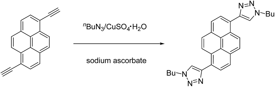
Fig. 1a displays the normalized one-photon absorption and fluorescence emission spectra of DTP in dichloromethane (CH2Cl2) solution. The one photon absorption exhibits one broad and structureless absorption band centred at 365 nm, which can be ascribed to the absorptive transition from the ground state S0 to the S1 state. There is a minor artifact in the UV-vis absorption spectrum at 365 nm, attributed to the switching between UV and visible light sources. Besides, the fluorescence excitation spectrum is similar to the one-photon absorption spectrum with a maximum at 365 nm (Fig. S2†). While the emission of the DTP solution exhibits a well resolved feature with emission peaks located at 402 nm (0–0), 424 nm (0–1) and 452 nm (0–2).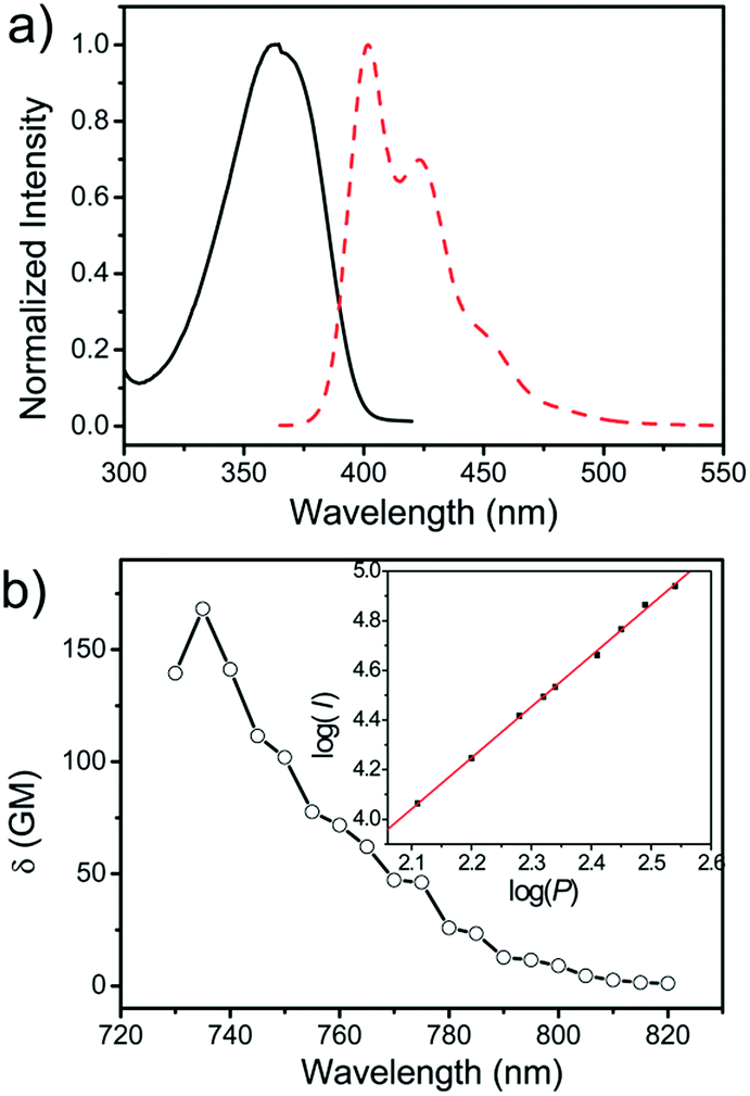 | ||
| Fig. 1 (a) Normalized one-photon UV-vis absorbance and fluorescence emission spectra (λex = 350 nm). (b) Two-photon-absorption cross section δ of DTP dissolved in CH2Cl2 (1 × 10⁻⁴ M). The inset shows the TPE induced fluorescence intensity (I) versus the incident laser power (P) for DTP molecules at the excitation wavelength of 740 nm. The slope obtained by linear fitting is 2.06 ± 0.03. | ||
Two-photon absorption (TPA) cross section δ of DTP (Fig. 1b) and two-photon excitation fluorescence (TPEF) spectra of DTP monomers dissolved in CH2Cl2 at 740 nm (Fig. S2†) were measured by the two-photon-induced fluorescence measurement technique using a Ti:sapphire laser as the excitation source over a relatively wide range of wavelengths between 730 and 820 nm, which avoids possible interference by excited state excitation. The maximal δ of DTP is as large as 168 GM (1 GM = 10−50 cm4 s per photon) at the wavelength of 735 nm as shown in Fig. 1b. The dependence of the two-photon induced fluorescence intensity on the input laser power is displayed in the inset of Fig. 1b. The experimental points can be well-fitted to a linear relationship with a slope of 2.06 ± 0.03, confirming the TPE origin of luminescence. The λmax/2 in the calculated two-photon absorption spectra is nearly the same as the one-photon absorption maxima, which predicts that the two-photon allowed states are similar to those of the one-photon allowed states. Moreover, the TPEF spectrum (Fig. S2†) exhibits little difference from that of the one-photon excitation fluorescence spectrum, revealing that the emission occurs from the same excited state regardless of the excitation mode. Besides, the fluorescence quantum yields (Φ) are also measured through a relative method for monomer using 9,10-diphenylanthracene as a reference and quantum yield (Φ) of DTP solution in CH2Cl2 is close to unity (0.99).
 | ||
| Fig. 2 (a) SEM image of DTP nanowires (b) TEM image of DTP nanowire; inset: SAED pattern of the nanowire. (c) Predicted Bravais–Friedel–Donnay–Harker (BFDH) crystal morphology of DTP using Materials Studio Software Package. (d) X-ray diffraction patterns of DTP nanowires and powder. | ||
3. Nanowire preparation and characteristic
Single-crystal DTP nanowires were prepared by a one-step anti-solvent diffusion method combined with solvent evaporation induced self-assembly. Typically, 50 μL of DTP of CH2Cl2/THF (v/v = 1![[thin space (1/6-em)]](https://www.rsc.org/images/entities/char_2009.gif) :1) solution (1 mM) was injected onto a quarts substrate which was then placed in a closed beaker (100 mL) containing 10 mL of toluene anti-solvent. During the above procedures, a solvent atmosphere was created and the evaporation speed of the solvent of DTP solution could be well-controlled. By altering the anti-solvents, nanowires with different lengths and diameters can be easily obtained (Fig. S3†). After complete evaporation of the solvent, well-defined 1D crystalline DTP nanowires were obtained.
:1) solution (1 mM) was injected onto a quarts substrate which was then placed in a closed beaker (100 mL) containing 10 mL of toluene anti-solvent. During the above procedures, a solvent atmosphere was created and the evaporation speed of the solvent of DTP solution could be well-controlled. By altering the anti-solvents, nanowires with different lengths and diameters can be easily obtained (Fig. S3†). After complete evaporation of the solvent, well-defined 1D crystalline DTP nanowires were obtained.
As shown in the scanning electron microscopy (SEM) image in Fig. 2a, the as-fabricated nanowires have high morphological purity with smooth surface and defect-free structure. The flatness of the surface is clearly illustrated in the atomic force microscopy (AFM) image, which has a typical height of 250 nm and width of 700 nm, as determined by the cross section analysis (Fig. S4†). The morphology of the wires was further confirmed by TEM. Inset of Fig. 2b displays the selected-area electron diffraction (SAED) pattern by directing the electron beam perpendicular to the flat faces of a single wire, which exhibits that the wires are single-crystalline rather than polycrystalline, as revealed by the sharp spots. The circled set of spot with d-spacing values of 7.5 Å is due to Bragg reflection and triangle set of spot with a d-spacing of 5.4 Å is assigned to reflections from {100} crystal planes. This result reveals that the DTP molecules within the wires prefer to arrange themselves along the crystal [100] direction, that is, the crystallographic a-axis direction. This is further verified by the X-ray diffraction (XRD) pattern (Fig. 2d), which is dominated by the {001} diffraction peak. Combining SAED and XRD results that the nanowires were determined to grow along the crystal a-axis with the side surfaces bound by (001) crystal facets. The molecular arrangement is exhibited as the calculated Bravais–Friedel–Donnay–Harker (BFDH) crystal morphology of DTP using Materials Studio Software Package (Fig. 2c).
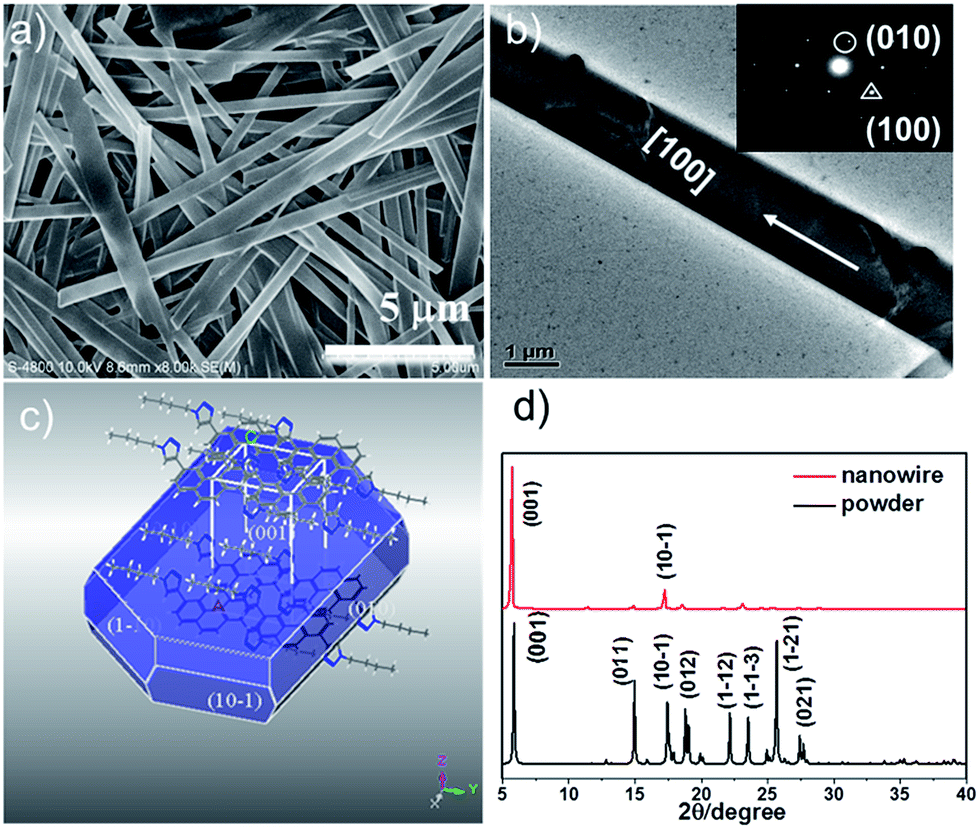
In the photoluminescent (PL) image (Fig. 3b) of DTP nanowires under unfocused UV irradiation (330–380 nm), an intense blue PL along the nanowires bodies with bright spots at both ends can be obviously observed. It is typical feature of optical waveguide that the PL energy can propagate efficiently along the nanowire growing direction. Fig. 3a shows that the two-photon fluorescence emission images of single nanowire upon a focused 800 nm femtosecond pulse laser excitation with bright PL spots at the tips and weaker emission from the bodies. The spatially resolved PL spectra of the emitted light with respect to the length travelled (between the excitation spot and the rod tip) were measured to gain further insight into the waveguide behaviour with the DTP nanowires (Fig. 3d). The inset of Fig. 3d displays a logarithmic scale of the whole area-integral intensity for each waveguided PL spectrum as a function of the propagation length, which clearly shows a linear decrease. The optical loss coefficient α of guided PL can be estimated according to the following equation:
| α = −10log(Iout/Iin)L−1 |
 | ||
| Fig. 3 (a) Schematic illustration of the experimental setup for optical waveguide measurement (b) PL image of DTP nanowires excited with the UV light (330–380 nm) (c) dark-field images were collected at five different positions of a single DTP nanowire upon excitation at 800 nm. (d) Spatially resolved PL spectra of the waveguided emission out-coupled at the tip of a single nanowire for different propagation distance. Inset shows logarithmic plot of the relative PL intensities at maximum versus the propagation distance. The scale bar is 10 μm labelled in the images. The filter used is 440 nm. | ||
4. Polarization of nanowire and fluorescence emission modulated
To obtain further insight about the optical characteristic of DTP nanowires, spatially-resolved PL spectra measurement of a single nanowire with many defects were carried out with an excitation wavelength of 760 nm. Two obvious fluorescence emission bands at 400–460 nm and 460–600 nm were observed, when the laser of excitation wavelength at 760 nm was employed. The former shorter wavelength emission band was ascribed to the monomer state of DTP and the latter one centered around 500 nm which become prominent compared to one-photon solution absorption in Fig. 1a is assigned to the aggregate state. It is noteworthy that not only monomer emission band but also aggregation emission was observed, which is a rare phenomenon in a defect-limited single crystalline nanowire. Therefore, an entirely possibility model is proposed from intuition that transition dipoles of monomer and aggregate are orthogonal to each other.In order to verify this hypothesis, polarized optical measurement was conducted. The parameter θ refers to the changed angle of linearly polarized light and the incident polarization, which was adjusted using a half-wave plate. Note that when the polarized light was changing from 0 to 90°, the intensity of shorter wavelength emission region was reduced and simultaneously the intensity of the longer wavelength region was increased. Fluorescence emission at 447 nm and 502 nm as two representative wavelengths of the two emission bands are selected to monitor the evolution of emission intensity over the degree θ of incidence polarized light changes. The emission intensity of 447 nm varied in an oscillatory manner between a maximum θ = 90° and minimum value θ = 0° (180°), while the emission intensity of 502 nm has the opposite behaviours, as illustrated in Fig. 4b. It exhibits an orthogonal polarized emission. This result has implied that DTP monomer and aggregate have orthogonal optical transition dipole.
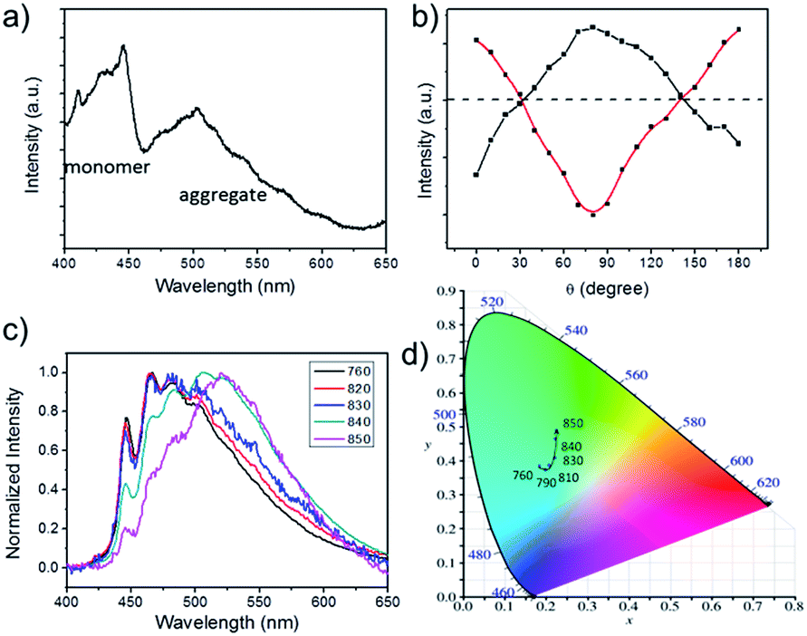 | ||
| Fig. 4 (a) Spatially resolved PL spectrum of a single nanowire upon excitation at 760 nm. (b) Peak intensities at 447 nm (red) and 502 nm (black) as a function of incident polarization angle. (c) Normalized solid-state spatially resolved PL spectra of a single DTP nanowire at various excitation wavelengths, 440 nm short pass filter. (d) The variation of the CIE coordinates with the different excitation wavelength. | ||
Take advantage of orthogonal optical transition dipole resulting in non-interfering emission bands of the monomer and aggregate of DTP. It is obvious that changing the excitation wavelength could adjust the ratio of fluorescence emission peaks of monomer and aggregate, further modulating the emission colour of luminescence. In a typical experiment, the excitation wavelength was changing from 760 nm to 850 nm, resulting in a red-shift of the main emission peak from 466 to 522 nm. And the CIE coordinates of the emission light calculated from the PL spectra (Fig. 4d) clearly showed variations of the output signals, which indicate that the PL emission shifted gradually from blue to green with the decrease of excitation energy.
Conclusions
In conclusion, we have prepared single-crystal nanowires based on a new two-photon absorption derivative DTP, synthesized via CuAAC reaction. These highly crystalline nanowires have smooth surfaces and flat end facets, which can act as active waveguides, with the low optical loss of 0.0217 dB μm−1. Furthermore, single-particle spectroscopy of nanowire clarifies that one short wavelength emission band ranging 400 to 460 nm results from DTP monomer and the other longer wavelength band around 500 nm is responsible for the aggregate state of DTP. Moreover, the two emission peak intensity of a single nanowire have opposite oscillatory manners by changing the polarization of the incident light, owning to the two orthogonal optical transition dipole of monomer and aggregate. Besides, the excitation wavelength was changing from 760 nm to 850 nm, resulting in a red-shift of the maximum emission peak from 466 to 522 nm and the variation of the CIE coordinates from blue to green. This simple synthesis combining novel optical properties would make the triazole-conjugated pyrene derivative promising for applications in nano-optical devices.Acknowledgements
This work was supported by National Natural Science Foundation of China (No. 21603008), the Open Project Program of Beijing Key Laboratory (Grant No. KYJD02150201, 2015A-48), Beijing Municipal Education Committee (Grant No. SQKM201610012006), and Research Project of Talent Introduction Found of Beijing Institute of Fashion Technology (Grant No. 2015A-16).Notes and references
- Z. Y. Yu, Y. S. Wu, Q. Liao, H. H. Zhang, S. M. Bai, H. Li, Z. Z. Xu, C. L. Sun, X. D. Wang, J. N. Yao and H. B. Fu, J. Am. Chem. Soc., 2015, 137, 15105–15111 CrossRef CAS PubMed.
- X. D. Wang, H. Li, Y. S. Wu, Z. Z. Xu and H. B. Fu, J. Am. Chem. Soc., 2014, 136, 16602–16608 CrossRef CAS PubMed.
- X. Wang, Q. Liao, H. Li, S. Bai, Y. Wu, X. Lu, H. Hu, Q. Shi and H. Fu, J. Am. Chem. Soc., 2015, 137, 9289–9295 CrossRef CAS PubMed.
- Y. L. Lv, L. L. Zhu, H. Liu, Y. S. Wu, Z. L. Chen, H. B. Fu and Z. Y. Tian, Anal. Chim. Acta, 2014, 839, 74–82 CrossRef CAS PubMed.
- L. Zhang, W. Hu, L. Yu and Y. Wang, Chem. Commun., 2015, 51, 4298–4301 RSC.
- P. Guo, G. Zhao, P. Chen, B. Lei, L. Jiang, H. Zhang, W. Hu and M. Liu, ACS Nano, 2014, 8, 3402–3411 CrossRef CAS PubMed.
- G. A. O'Brien, A. J. Quinn, D. A. Tanner and G. Redmond, Adv. Mater., 2006, 18, 2379–2383 CrossRef.
- S. Schols, S. Verlaak, C. Rolin, D. Cheyns, J. Genoe and P. Heremans, Adv. Funct. Mater., 2008, 18, 136–144 CrossRef CAS.
- Y. S. Zhao, J. Xu, A. Peng, H. Fu, Y. Ma, L. Jiang and J. Yao, Angew. Chem., 2008, 120, 7411–7415 CrossRef.
- C.-A. Di, F. Zhang and D. Zhu, Adv. Mater., 2013, 25, 313–330 CrossRef CAS PubMed.
- H. Dong, H. Zhu, Q. Meng, X. Gong and W. Hu, Chem. Soc. Rev., 2012, 41, 1754–1808 RSC.
- S. Z. Bisri, C. Piliego, J. Gao and M. A. Loi, Adv. Mater., 2014, 26, 1176–1199 CrossRef CAS PubMed.
- W. Yue, T. He, M. Stolte, M. Gsanger and F. Wurthner, Chem. Commun., 2014, 50, 545–547 RSC.
- K. Takazawa, Y. Kitahama, Y. Kimura and G. Kido, Nano Lett., 2005, 5, 1293–1296 CrossRef CAS PubMed.
- Y. S. Zhao, H. Fu, A. Peng, Y. Ma, Q. Liao and J. Yao, Acc. Chem. Res., 2009, 43, 409–418 CrossRef PubMed.
- C. W. Spangler, J. Mater. Chem., 1999, 9, 2013–2020 RSC.
- C. Zhang, C.-L. Zou, Y. Yan, R. Hao, F.-W. Sun, Z.-F. Han, Y. S. Zhao and J. Yao, J. Am. Chem. Soc., 2011, 133, 7276–7279 CrossRef CAS PubMed.
- D. A. Parthenopoulos and P. M. Rentzepis, Science, 1989, 245, 843–845 CAS.
- C. N. LaFratta, J. T. Fourkas, T. Baldacchini and R. A. Farrer, Angew. Chem., 2007, 119, 6352–6374 CrossRef.
- Z. Xu, Q. Liao, Y. Wu, W. Ren, W. Li, L. Liu, S. Wang, Z. Gu, H. Zhang and H. Fu, J. Mater. Chem., 2012, 22, 17737–17743 RSC.
- G. Wang, X. Zhang, J. Geng, K. Li, D. Ding, K.-Y. Pu, L. Cai, Y.-H. Lai and B. Liu, Chem.–Eur. J., 2012, 18, 9705–9713 CrossRef CAS PubMed.
- J. Arnbjerg, A. Jiménez-Banzo, M. J. Paterson, S. Nonell, J. I. Borrell, O. Christiansen and P. R. Ogilby, J. Am. Chem. Soc., 2007, 129, 5188–5199 CrossRef CAS PubMed.
- F. Gao, Q. Liao, Z.-Z. Xu, Y.-H. Yue, Q. Wang, H.-L. Zhang and H.-B. Fu, Angew. Chem., Int. Ed., 2010, 49, 6243 CrossRef.
- K. D. Belfield, M. V. Bondar, F. E. Hernandez and O. V. Przhonska, J. Phys. Chem. C, 2008, 112, 5618–5622 CAS.
- M. Hara, S. Tojo, K. Kawai and T. Majima, Phys. Chem. Chem. Phys., 2004, 6, 3215–3220 RSC.
- H. Maeda, T. Maeda, K. Mizuno, K. Fujimoto, H. Shimizu and M. Inouye, Chem.–Eur. J., 2006, 12, 824–831 CrossRef CAS PubMed.
- L. Wang, W.-W. Yang, R.-H. Zheng, Q. Shi, Y.-W. Zhong and J. Yao, Inorg. Chem., 2011, 50, 7074–7079 CrossRef CAS PubMed.
- D. O'Carroll, I. Lieberwirth and G. Redmond, Small, 2007, 3, 1178–1183 CrossRef PubMed.
- Q. Bao, B. M. Goh, B. Yan, T. Yu, Z. Shen and K. P. Loh, Adv. Mater., 2010, 22, 3661–3666 CrossRef CAS PubMed.
Footnote |
| † Electronic supplementary information (ESI) available: Experimental details and measurements. See DOI: 10.1039/c7ra02406a |
| This journal is © The Royal Society of Chemistry 2017 |