 Open Access Article
Creative Commons Attribution 3.0 Unported Licence
Improved interface of ZnO/CH3NH3PbI3 by a dynamic spin-coating process for efficient perovskite solar cells†
Feng Yanga,
Dong-Won Kang *b and
Yong-Sang Kim
 *a
*a
aSchool of Electronic and Electrical Engineering, Sungkyunkwan University, Suwon, Gyeonggi 440-746, Republic of Korea. E-mail: yongsang@skku.edu
bDepartment of Solar & Energy Engineering, Cheongju University, Cheongju, Chungbuk 363-764, Republic of Korea. E-mail: kang@cju.ac.kr
First published on 30th March 2017
Abstract
For low-temperature solution-processed perovskite solar cells, ZnO as an electron transport layer (ETL) has been studied instead of TiO2 requiring high sintering temperature. However reports have been scarce about successful fabrication of perovskite solar cells based on the solution-processed ZnO ETL under atmospheric air. In this study, we found a possible mechanism to cause poor performance of the perovskite solar cells, which can be ascribed to chemical reactions between the methylammonium iodide (MAI) of the perovskite precursor (MAPbI3) solution and the ZnO film under humid conditions. The MAI solution could etch out ZnO ETL and promote serious carrier recombination if processed in air, whereas there was no such reaction for processing in a glovebox (H2O < 0.1 ppm). In order to suppress the reactions in air-ambient, we applied a simple and novel dynamic spin-coating process, dripping the perovskite precursor solution on ZnO during the spin-coating process, followed by an anti-solvent washing treatment. Using this approach, for the first time, the interfacial reaction of ZnO/MAPbI3 was significantly suppressed and thus a power conversion efficiency of the perovskite solar cells fully-processed in air-ambient was enhanced from 0% to 11.2%. These experimental results pave the way for the development of perovskite solar cells under low-temperature processing in air-ambient.
1 Introduction
Perovskite (PRV) solar cells have recently reached over 20.0% of power conversion efficiency (PCE),1,2 while the world record is 22.1%.3 The advantage of perovskite materials is their solution process capability. An efficient perovskite solar cell consists of cathode/ETL/perovskite/HTL/anode, where ETL is the electron transport layer and HTL is the hole transport layer. The HTL and ETL not only extract the hole and electron currents, but also prevent the perovskite layer from direct contact with the electrodes to reduce charge recombination photocurrent. For the electron transport materials, many robust and stable metal oxide based ETLs have been involved in perovskite solar cells, such as titanium dioxide (TiO2),3,4 tungsten oxide (WOX),5 and zinc oxide (ZnO).6,7 Among the metal oxides, TiO2 has been popular as ETL.2,8 However, TiO2 ETL needs a high sintering temperature treatment at 450–500 °C to be sufficiently conductive.9 Such a high temperature also would not be suitable for the commercial application of perovskite solar cells.10Recently, solution-processed ETL of ZnO with low-temperature thermal treatment has been applied in the development of perovskite solar cells.6,7,11 ZnO ETL could be processed at low temperature with efficient electron transport property, and be an excellent candidate to replace the TiO2 ETL used in perovskite solar cells.12 The solution-processed ZnO ETLs in the perovskite solar cells are similar to those in organic photovoltaic cells, with sol–gel ZnO solution,13 or ZnO nanoparticle solution.14 Several ZnO nanoparticles (NPs) have been used in the perovskite solar cells, which are usually synthesized by complex procedures that include long reaction time, precipitation, washing, and dilution processes.7,15 In contrast, sol–gel processed ZnO ETL has the advantages of simple synthesis, long-term stability, and low-temperature process.16 One of the typical perovskite solar cells is designed by spin-coating a CH3NH3PbI3 precursor solution onto a ETL, followed by thermal treatment at about 100 °C, and subsequent deposition of HTLs.17,18 In order to introduce low-temperature solution-processed ZnO ETL into perovskite solar cells, both a one-step spin-coating and a two-step procedure for perovskite layer have been studied.
Unfortunately, the solution-processed ZnO surface is rich in hydroxyl groups and/or residual acetate ligands, which could lead to decomposition of the perovskite film into methylamine and PbI2.14,15 In the one-step spin-coating procedure, Reddy et al. fabricated some efficient ZnO-based perovskite solar cells in a glovebox.19 And Zuo et al. enhanced the PCE of the ZnO-based perovskite solar cells by interfacial engineering.13 But attempts to deposit perovskite films directly on the ZnO surface by a one-step spin-coating process under ambient air have met with failure.6 There might be some interface issues between the ZnO and perovskite materials. However, for the deposition of perovskite films onto these ZnO layers, the two-step deposition method worked;20–23 spin-coated PbI2 thin films were immersed in a solution of CH3NH3I (MAI), converting them to the perovskite. Nevertheless, the one-step method recently becomes very popular way to fabricate the high performance perovskite solar cells, because it is very easy to get efficient perovskite film via one-step method by solvents engineering, solvent treatment, or perovskite material engineering.24
For the one-step spin-coated perovskite film under ambient air, the interface issue of perovskite films and the ZnO films should either be avoided or controlled at a low level. In the study, we systematically confirmed that MAI solution in perovskite precursor solution reacts with the underlying ZnO, which results in an etching effect on the ZnO. Then, the perovskite layer could directly contact the ITO electrode, which causes a severe charge recombination. We developed a simple and novel dynamic spin-coating process to improve the interface of perovskite absorber and the ZnO ETL under ambient air, which contributed to successful operation of the perovskite solar cells.
2 Experimental section
2.1 Materials
Methylammonium iodide (MAI, 99.99%, LT-S9126) was purchased from Luminescence Technology Corp., PbI2 (99%) from Sigma Aldrich, and poly(3-hexylthiophene) (P3HT) from Rieke Metals. The indium tin oxide (ITO) coated glass was supplied by Fine Chemicals (South Korea) (15 Ω per square sheet resistance, and 0.7 mm thickness). Anhydrous chlorobenzene (CB, 99.9%), dimethylformamide (DFM, ACS reagent ≥ 99.8%), and dimethyl sulfoxide (DMSO, ≥99.9%) were from Sigma Aldrich. Gold (Au) was from Vacuum Thin Film Materials Co. (South Korea). Zinc acetate dihydrate (99.999%), monoethanolamine (MEA, ACS reagent, 99.0%), and 2-methoxyethanol (2-ME, anhydrous, 99.8%) were from Sigma Aldrich. The vapor pressures of the solvents, the decomposition temperature, and the melting points of solid materials come from safety data sheets of Sigma Aldrich.2.2 Solutions for the perovskite solar cells
(1) 50 wt% perovskite solution of MAI![[thin space (1/6-em)]](https://www.rsc.org/images/entities/char_2009.gif) :
:![[thin space (1/6-em)]](https://www.rsc.org/images/entities/char_2009.gif) PbI2
PbI2![[thin space (1/6-em)]](https://www.rsc.org/images/entities/char_2009.gif) :
:![[thin space (1/6-em)]](https://www.rsc.org/images/entities/char_2009.gif) DMSO 1
DMSO 1![[thin space (1/6-em)]](https://www.rsc.org/images/entities/char_2009.gif) :
:![[thin space (1/6-em)]](https://www.rsc.org/images/entities/char_2009.gif) 1
1![[thin space (1/6-em)]](https://www.rsc.org/images/entities/char_2009.gif) :
:![[thin space (1/6-em)]](https://www.rsc.org/images/entities/char_2009.gif) 0.6. 0.161 g MAI and 0.472 g PbI2 were dissolved in 0.600 ml DMF and 0.0434 ml DMSO, and stirred at 1500 rpm and 65 °C on a hotplate overnight. A yellow and turbid solution was obtained. The recipes of other perovskite precursor solutions are as similar as this recipes but with different component ratios. (2) P3HT solution: 0.015 g P3HT in 1 ml chlorobenzene was stirred at room temperature overnight. (3) ZnO solution: the 0.5 M precursor solution consisting of 0.220 g zinc acetate dihydrate and 61.0 μl monoethanolamine in 2 ml 2-methoxyethanol was stirred at room temperature overnight.
0.6. 0.161 g MAI and 0.472 g PbI2 were dissolved in 0.600 ml DMF and 0.0434 ml DMSO, and stirred at 1500 rpm and 65 °C on a hotplate overnight. A yellow and turbid solution was obtained. The recipes of other perovskite precursor solutions are as similar as this recipes but with different component ratios. (2) P3HT solution: 0.015 g P3HT in 1 ml chlorobenzene was stirred at room temperature overnight. (3) ZnO solution: the 0.5 M precursor solution consisting of 0.220 g zinc acetate dihydrate and 61.0 μl monoethanolamine in 2 ml 2-methoxyethanol was stirred at room temperature overnight.
2.3 Perovskite solar cells fabrication
The ITO substrates were ultra-sonicated for 15 min in deionized water, followed by acetone, and then isopropyl alcohol (IPA). All the cleaned ITO substrates were dried in an oven at 75 °C for 30 min, and then kept overnight. The ZnO 0.5 M precursor solution after filtering was spin-coated on the ITO substrates at 4000 rpm for 40 s. The wet ZnO films were annealed at 160 °C in the oven for 10 min. 50 nm dense ZnO films were obtained. The spin coating of 50 wt% perovskite solution filtered with PVDF filter was carried out in a special dynamic mode. The dynamic spin-coating process was involved first starting the substrate spinning, and allowing it to reach the desired spin speed, before the perovskite solution was dispersed onto the ZnO substrate. 35 μl of perovskite solution was dripped onto the ZnO coated substrate by the dynamic spin-coating process, and the washing treatment with CB of 200 μl was carried out by pipette tips during the rotation of perovskite coating, 5 s after starting the dripping of perovskite solution. All the wet light red perovskite films were annealed at 90 °C, for 60 min. 50 μl P3HT solution, 15 mg ml−1 in CB, was spin-coated on the perovskite film at 2000 rpm for 25 s. Finally, Au electrode was deposited by thermal evaporator. After the thermal deposition of ∼50 nm thick Au film through a shadow mask, the devices were finished for measurement. All fabrication processes were carried out in ambient air. The active area of each device was 0.1 cm2.2.4 Device characterization
The current density–voltage (J–V) characterization of the devices was measured by J–V curve tracer (Eko MP-160) and solar simulator (Yss-E40, Yamashita Denso) under AM 1.5G irradiation with the intensity of 100 mW cm−2, calibrated by a Newport certified standard silicon cell. Fourier transform infrared spectra (FT-IR) were scanned with a resolution of 8 cm−1 by Bruker IFS-66/S FTIR. Optical microscopy images were obtained using an Olympus BX51 Microscope Digital Camera. Atomic force microscopy (AFM) images were obtained with advanced scanning probe microscopes (PSIA Corp). The thicknesses of all films were characterized by the AFM system.3 Results and discussion
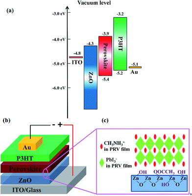
Fig. 1(a) and (b) show the energy level diagram and device structure of PRV devices, respectively. A general structure of ITO/ZnO/CH3NH3PbI3/P3HT/Au was designed. Solution-processed ZnO layer in the PRV cells plays a role as the electron transport layer and hole blocking layer, and the P3HT as the hole transport layer. The PRV films were fabricated on low-temperature solution-processed ZnO films via a special dynamic spin-coating procedure with a one-step method. Compared with the dynamic spin-coating, a static spin-coating processed PRV film was first investigated on the solution-processed ZnO film. Table 1 shows that the static spin-coated PRV cell displayed very poor performance (device static 40 wt%). Its open-circuit voltage (VOC) is 0.01 V, much smaller than the normal value of 0.9 V,25 which indicates that the hole blocking layer of ZnO does not block the charge recombination of electrons and holes. We presumed that the ZnO layer in the static spin-coated PRV cell was etched off during the spin-coating process of the PRV wet film.![[thin space (1/6-em)]](https://www.rsc.org/images/entities/char_2009.gif) :
:![[thin space (1/6-em)]](https://www.rsc.org/images/entities/char_2009.gif) PbI2
PbI2![[thin space (1/6-em)]](https://www.rsc.org/images/entities/char_2009.gif) :
:![[thin space (1/6-em)]](https://www.rsc.org/images/entities/char_2009.gif) DMSO in the PRV solution
DMSO in the PRV solution
| Devices | JSC [mA cm−2] | VOC [V] | FF | PCE [%] |
|---|---|---|---|---|
Static 40 wt% with 1![[thin space (1/6-em)]](https://www.rsc.org/images/entities/char_2009.gif) : :![[thin space (1/6-em)]](https://www.rsc.org/images/entities/char_2009.gif) 1 1![[thin space (1/6-em)]](https://www.rsc.org/images/entities/char_2009.gif) : :![[thin space (1/6-em)]](https://www.rsc.org/images/entities/char_2009.gif) 1 1 |
1.56 (±0.41) | 0.01 (±0.01) | 0.29 (±0.05) | 0.00 (±0.00) |
Dynamic 1 40 wt% with 1![[thin space (1/6-em)]](https://www.rsc.org/images/entities/char_2009.gif) : :![[thin space (1/6-em)]](https://www.rsc.org/images/entities/char_2009.gif) 1 1![[thin space (1/6-em)]](https://www.rsc.org/images/entities/char_2009.gif) : :![[thin space (1/6-em)]](https://www.rsc.org/images/entities/char_2009.gif) 1 1 |
13.40 (±0.61) | 0.86 (±0.01) | 0.58 (±0.03) | 6.67 (±0.44) |
Dynamic 2 50 wt% with 1![[thin space (1/6-em)]](https://www.rsc.org/images/entities/char_2009.gif) : :![[thin space (1/6-em)]](https://www.rsc.org/images/entities/char_2009.gif) 1 1![[thin space (1/6-em)]](https://www.rsc.org/images/entities/char_2009.gif) : :![[thin space (1/6-em)]](https://www.rsc.org/images/entities/char_2009.gif) 1 1 |
16.00 (±0.77) | 0.88 (±0.01) | 0.61 (±0.03) | 8.56 (±0.44) |
Dynamic 2 50 wt% with 1![[thin space (1/6-em)]](https://www.rsc.org/images/entities/char_2009.gif) : :![[thin space (1/6-em)]](https://www.rsc.org/images/entities/char_2009.gif) 1 1![[thin space (1/6-em)]](https://www.rsc.org/images/entities/char_2009.gif) : :![[thin space (1/6-em)]](https://www.rsc.org/images/entities/char_2009.gif) 0.6 0.6 |
18.67 (±0.19) | 0.91 (±0.00) | 0.66 (±0.00) | 11.23 (±0.15) |
3.1 Low-temperature solution processed ZnO film
We found some chemical reaction between the ZnO layer and PRV solution. In order to understand the reaction, the ZnO layer was carefully studied. Fig. 2 shows a sketch of the chemical equilibria in the ZnO precursor solution. The chemistry of the ZnO precursor solution has been well studied by several groups.26–29 Stirring the precursor solution overnight results in the formation of translucent solution by forced hydrolysis of zinc ion complexes, and the necessary water for the hydrolysis is supplied by the hydrated salt. Zinc ion readily forms complex ions in the aqueous amine, as shown in the 4 steps in Fig. 2. The 4-step processes are proposed as follows:
Zn(CH3COO)2·2H2O ![[left over right harpoons]](https://www.rsc.org/images/entities/char_21cb.gif) Zn(CH3COO)2 + 2H2O Zn(CH3COO)2 + 2H2O
| (1) |
Zn(CH3COO)2 + 2H2O ![[left over right harpoons]](https://www.rsc.org/images/entities/char_21cb.gif) 2CH3COOH + Zn(OH)2 2CH3COOH + Zn(OH)2
| (2) |
Zn(OH)2 + 4NH2CH2CH2OH (MEA) ![[left over right harpoons]](https://www.rsc.org/images/entities/char_21cb.gif) [Zn(NH2CH2CH2OH)4]2+ + 2OH− [Zn(NH2CH2CH2OH)4]2+ + 2OH−
| (3) |
Zn(OH)2 + 2OH− ![[left over right harpoons]](https://www.rsc.org/images/entities/char_21cb.gif) [Zn(OH)4]2−. [Zn(OH)4]2−.
| (4) |
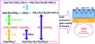 | ||
| Fig. 2 Sketch of the chemical equilibria taking place in the ZnO precursor solution and ZnO film. The hydrolysis is about 4 steps, ①, ②, ③, and ④. The spin-coating process encourages hydrolysis. | ||
The precursor is spin-coated onto the cleaned ITO substrates. The vapor pressures of CH3COOH, 2-ME, and MEA in the ZnO precursor solution respectively are 11.4, 6.17, and 0.2 mmHg, respectively, at 20 °C. The acetic acid first vaporizes out of the wet ZnO film, which makes the hydrolysis produce more zinc hydroxide (Zn(OH)2) in eqn (2). 2-ME then vaporizes out of the wet film during the spin-coating. With thermal treatment of the wet ZnO precursor films at 160 °C, the MEA and acetic acid vaporize out of the wet film and leave an intermediate phase of Zn(OH)2, and the Zn(OH)2 film is converted into ZnO film, as shown in eqn (5):
| Zn(OH)2 → ZnO + H2O. | (5) |
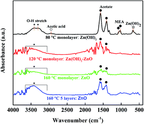
Some surface groups, such as hydroxide or acetate, are on the surface or inside of the ZnO film. The hydroxide group was characterized by X-ray photoelectron spectroscopy (XPS) by some groups.14,28,29 We investigated the spin-coated ZnO films by FTIR measurement, of which Fig. 3 shows the spectra. There are two typical vibrational modes at 1574 and 1408 cm−1, which are ascribed to the stretching vibration of C![[double bond, length as m-dash]](https://www.rsc.org/images/entities/char_e001.gif) O and C–O, respectively, in the acetate group.6,15,30,31 Moreover, the wide band around 3400 cm−1 is responsible for the hydroxyl group.6,30,32 When the ZnO wet films are annealed at 80, 120, and 160 °C, the hydroxyl stretch gradually decreases as the temperature decreases, as do the acetate stretching bands (as shown in Fig. 3). By annealing at 80 °C, the Zn(OH)2 monolayer was obtained with essential absorption of hydroxyl groups at 3414 and 3310 cm−1, and clear absorption peaks of acetate group at 1574 and 1408 cm−1. The peaks at 1072 and 1026 cm−1 come from the C–N and C–O stretching, respectively, of the residual MEA. The weak peak at 2947 cm−1 is due to the C–H stretching of acetic acid.33 There is also small absorption at 671 cm−1, which comes from the stretching and bending modes of Zn-hydroxide.32 When the spin-coated ZnO wet film was annealed at 120 °C, the zinc acetate could transform into Zn(OH)2. Then the Zn(OH)2 is transformed into ZnO since the absorption of the hydroxide group at about 3400 cm−1 decreases and shifts blue. By annealing at 160 °C, the monolayer ZnO film has no essential hydroxyl groups and is transformed into ZnO phase. Fig. 3 shows that the absorption of hydroxide and acetate groups appears again in the 5-layer ZnO film (repeating the ZnO monolayer fabrication process 5 times). This also confirmed that the solution-processed ZnO film has surface groups of hydroxide and acetate, as Fig. 2 shows.
O and C–O, respectively, in the acetate group.6,15,30,31 Moreover, the wide band around 3400 cm−1 is responsible for the hydroxyl group.6,30,32 When the ZnO wet films are annealed at 80, 120, and 160 °C, the hydroxyl stretch gradually decreases as the temperature decreases, as do the acetate stretching bands (as shown in Fig. 3). By annealing at 80 °C, the Zn(OH)2 monolayer was obtained with essential absorption of hydroxyl groups at 3414 and 3310 cm−1, and clear absorption peaks of acetate group at 1574 and 1408 cm−1. The peaks at 1072 and 1026 cm−1 come from the C–N and C–O stretching, respectively, of the residual MEA. The weak peak at 2947 cm−1 is due to the C–H stretching of acetic acid.33 There is also small absorption at 671 cm−1, which comes from the stretching and bending modes of Zn-hydroxide.32 When the spin-coated ZnO wet film was annealed at 120 °C, the zinc acetate could transform into Zn(OH)2. Then the Zn(OH)2 is transformed into ZnO since the absorption of the hydroxide group at about 3400 cm−1 decreases and shifts blue. By annealing at 160 °C, the monolayer ZnO film has no essential hydroxyl groups and is transformed into ZnO phase. Fig. 3 shows that the absorption of hydroxide and acetate groups appears again in the 5-layer ZnO film (repeating the ZnO monolayer fabrication process 5 times). This also confirmed that the solution-processed ZnO film has surface groups of hydroxide and acetate, as Fig. 2 shows.
3.2 Reactions between perovskite precursor solution and the ZnO film in ambient air
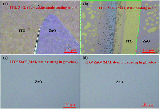
Interestingly, the ZnO film is very sensitive to the PRV precursor solution, which is made of MAI, PbI2, DMSO and DMF. We found that the PbI2, DMSO and DMF are friendly to the ZnO film (see ESI Fig. S1(a)†), but the MAI could etch off the ZnO film from the ITO substrate (see ESI Fig. S1(b)†). This etching effect could be clearly determined from Fig. 4. Fig. 4(a), shows that the perovskite precursor solution was dropped onto the ZnO film (the ZnO film was not fully covered), and then the spin-coating process started, which was the so-called “static” spin-coating process. After carefully washing with acetone and IPA, a little ZnO film was left on the ITO substrate, but most of the ZnO layer was etched off the ITO substrate. In Fig. 4(b), before starting the spin-coating process, the surface of ZnO layer within the green form was covered with a drop of MAI solution. There was some edge area of one small drop of MAI solution on ZnO film, which was the multi-interface of MAI solution, ZnO film, and air. Near this edge area, the etching effect of MAI was very clear on the ZnO film. The reaction between MAI and ZnO film was much more severe in the multi-interface area. We hypothesized that the enhanced reaction comes from the moisture. The H2O from air would heavily enhance the reaction between MAI and the ZnO film, because the ZnO with the surface groups (see Fig. 1(c)) easily starts the reaction. The hydroxide and acetate groups of ZnO film could react with MAI solution, similar to those shown in eqn (2)–(4), when the moisture is involved, as shown in eqn (2), (4), and (6):| Zn(OH)2 + 4CH3NH2·HI (MAI) → [Zn(CH3NH2·HI)4]2+ + 2OH−. | (6) |
The reaction between MAI and ZnO film was further studied with 0.1, 0.2, 0.6, and 1.0 M of MAI in DMF solution. The ZnO surfaces were heavily damaged when the concentration of MAI solutions was more than 0.2 M (see Fig. S2 in ESI†). The ZnO surface was not much changed when 0.1 M MAI solution was dropped onto and spread out on the ZnO film. But the 0.2 M MAI solution spread out easily on the ZnO film, and led to much absorption of moisture into the interface of ZnO and MAI, which enhanced the reaction of MAI and ZnO. During the spin-coating process, the path of moisture from air to the interface became very short, and moisture was very easily absorbed on the surface, and enhanced the reaction of ZnO and MAI. In order to support the above hypothesis of the moisture effect, we performed several tests of the reaction of MAI and ZnO in a glovebox (H2O < 0.1 ppm), and found that the reaction was totally suppressed. Fig. 4(c) and (d) show the static spin-coating process and the dynamic spin-coating process of 1.0 M MAI solution on ZnO films carried out in a glovebox. Interestingly, there was no damage to the ZnO surfaces for all the cases in the glovebox. Thus, it could be manifested that the reaction of MAI and ZnO was very limited, since the moisture was very low in the glovebox (H2O < 0.1 ppm). The reaction in ambient air was related to the moisture.
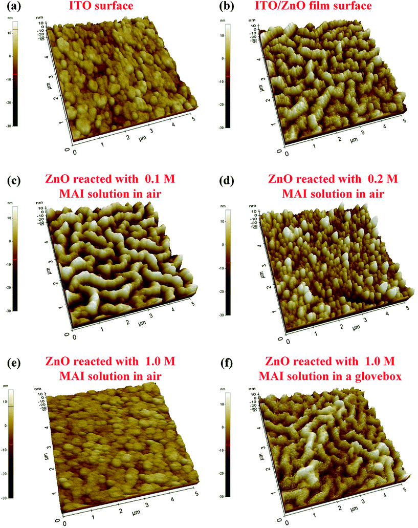
Fig. 5 shows that the ZnO surface treated with MAI solution in air or glovebox were carefully studied by AFM images (AFM topography images are shown in Fig. S3†). ZnO surface with nano-ridge structure34 was clearly found, compared with the ITO surface in Fig. 5(b). The root mean square roughness (RMS) of nano-ridge ZnO surface is 5.5 nm, which is higher that of ITO surface of 3.2 nm. The reaction of MAI and ZnO in glovebox is substantially suppressed, since there is no difference in nano-ridge ZnO surface topography or RMS values with or without MAI treatment, as shown in Fig. 5(f). Fig. 5(c)–(e) show that the MAI treated ZnO surfaces in ambient air greatly changed with various concentrations of MAI solution. The 0.1 M MAI solution slightly etched the ZnO surface. Comparing Fig. 5(b) and (c), small ZnO grains in the nano-ridge structure were etched off, and the RMS value of ZnO film with the MAI treatment increased from 5.5 to 7.3 nm. The etching effect of MAI solution of 0.2 and 1.0 M on ZnO was strong on the nano-ridge structured ZnO, and after the MAI treatment the nano-ridge ZnO surface disappeared, as Fig. 5(d) and (e) show. The RMS of the Fig. 5(e) was 2.4 nm, very similar as RMS of the bare ITO surface (Fig. 5(a)), 3.2 nm. And the surface morphology of the ITO/ZnO film surface, reacted with 1.0 M MAI solution in air, is similar as that of the bare ITO. Comparing the RMS and the surface morphology of 1.0 M MAI solution treated ITO/ZnO surface in air (Fig. 5(e)) and that in glovebox (Fig. 5(f)), we can clearly conclude that the ZnO nano-ridges disappeared after 1 M MAI treatment in air. Recalling all mentions above, we found that when it fabricated in the ambient air, the MAI of perovskite precursor solution has a strong reaction with the solution-processed ZnO film.
3.3 Dynamic spin-coating process for efficient perovskite solar cells
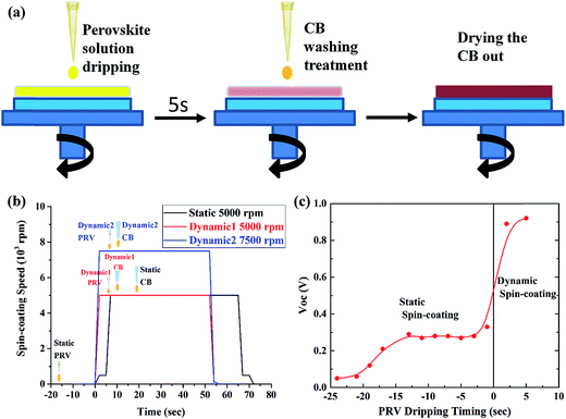
We developed a special dynamic spin-coating process for the working PRV device, which could limit the reaction between the MAI and ZnO as much as possible. Fig. 6(a) shows the dynamic process. We first started the spinning, and allowed it to reach the desired spin speed, before the PRV solution was dispersed onto the ZnO substrates. The perovskite solution was then dripped onto the spinning ZnO film. At this moment, most of the PRV solution was spun off the ZnO film, and a wet PRV film was left on the ZnO. After 5 s, a CB washing treatment was carried out, which was dripping CB on the wet PRV film before it turned turbid. The CB droplets led to the wet PRV film immediately freezing the constituents. In this process, the MAI and PbI2 crystallized together into the perovskite crystals, in which the MAI was frozen into the lattice site of the PRV crystals (as Fig. 1(c) shows). The surface of the wet PRV film was covered with CB, which was hydrophobic, and prevented moisture entering into the interface of MAI and ZnO. Then the CB was dried out of the wet PRV film. Fig. 6(a) and (b) show the dynamic spin-coating process. Fig. 6(c) shows the clear effect on the VOC from static spin-coating to dynamic spin-coating. For the static case, the PRV solution was dripped onto the ZnO film a few seconds before spin-coating (the static 5000 rpm in Fig. 6(b)). The reaction between MAI and ZnO was very active after more than five seconds of PRV solution dwelling time, since the moisture was easily absorbed into PRV solution. The ZnO film, as an electron transport layer and hole blocking layer in the PRV devices, was etched off after the static spin-coating process. This would lead to a very low VOC, as Fig. 6(c) shows. But for the dynamic spin-coating process, in a very short time, the MAI was frozen into perovskite crystals with the CB washing treatment and the reaction of MAI and ZnO was limited. After the dynamic spin-coating process, the ZnO film survived in the PRV device. Fig. 6(c) shows that PRV devices from dynamic spin-coating process have a good VOC of about 0.9 V.3.4 Efficient perovskite solar cells with improved interface of ZnO/perovskite materials
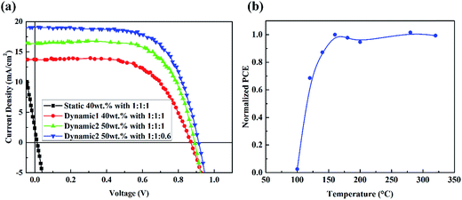
Table 1 shows that dynamic spin-coating process achieved high PCE of PRV devices with improved interface of ZnO/perovskite materials. The PRV solar cells have an average PCE of 11.23%, with JSC = 18.67 mA cm−2, VOC = 0.91 V, and FF = 0.66. When the concentration of PRV solution is increased from 40 to 50 wt%, the spin-coating speed for PRV film shifts from 5000 to 7500 rpm. This comes from the DMSO issue. Table 2 shows the recipes of PRV solutions for PRV devices. In the PRV solution, DMF is the main solvent, and DMSO the additive, which could form an adduct of MAI·PbI2·DMSO.35 The adduct formation weakens the reaction of MAI and ZnO, which could save the ZnO layer much more. Thus, the ratio of MAI![[thin space (1/6-em)]](https://www.rsc.org/images/entities/char_2009.gif) :
:![[thin space (1/6-em)]](https://www.rsc.org/images/entities/char_2009.gif) PbI2
PbI2![[thin space (1/6-em)]](https://www.rsc.org/images/entities/char_2009.gif) :
:![[thin space (1/6-em)]](https://www.rsc.org/images/entities/char_2009.gif) DMSO is set to 1
DMSO is set to 1![[thin space (1/6-em)]](https://www.rsc.org/images/entities/char_2009.gif) :
:![[thin space (1/6-em)]](https://www.rsc.org/images/entities/char_2009.gif) 1
1![[thin space (1/6-em)]](https://www.rsc.org/images/entities/char_2009.gif) :
:![[thin space (1/6-em)]](https://www.rsc.org/images/entities/char_2009.gif) 1. A washing window is set from the beginning of spinning to the wet PRV film becoming turbid. When the concentration of the PRV solution increase to 50 wt%, the washing window shifts from 14 to 16 s. More DMSO in the PRV solution makes the washing window shift more, because the DMSO will vaporize out after the DMF during the spin-coating process since the vapor pressure of DMSO is 0.42 mmHg at 20 °C, less than that of DMF of 2.7 mmHg. The longer time delay of the wet PRV film on the ZnO layer before the CB washing treatment would increase the possibility of the reaction of MAI and ZnO, and absorption of moisture from the air. Counting all these issues, better PRV devices are achieved with increasing the spin-coating speed to 7500 rpm, and optimizing the ratio of MAI
1. A washing window is set from the beginning of spinning to the wet PRV film becoming turbid. When the concentration of the PRV solution increase to 50 wt%, the washing window shifts from 14 to 16 s. More DMSO in the PRV solution makes the washing window shift more, because the DMSO will vaporize out after the DMF during the spin-coating process since the vapor pressure of DMSO is 0.42 mmHg at 20 °C, less than that of DMF of 2.7 mmHg. The longer time delay of the wet PRV film on the ZnO layer before the CB washing treatment would increase the possibility of the reaction of MAI and ZnO, and absorption of moisture from the air. Counting all these issues, better PRV devices are achieved with increasing the spin-coating speed to 7500 rpm, and optimizing the ratio of MAI![[thin space (1/6-em)]](https://www.rsc.org/images/entities/char_2009.gif) :
:![[thin space (1/6-em)]](https://www.rsc.org/images/entities/char_2009.gif) PbI2
PbI2![[thin space (1/6-em)]](https://www.rsc.org/images/entities/char_2009.gif) :
:![[thin space (1/6-em)]](https://www.rsc.org/images/entities/char_2009.gif) DMSO to 1
DMSO to 1![[thin space (1/6-em)]](https://www.rsc.org/images/entities/char_2009.gif) :
:![[thin space (1/6-em)]](https://www.rsc.org/images/entities/char_2009.gif) 1
1![[thin space (1/6-em)]](https://www.rsc.org/images/entities/char_2009.gif) :
:![[thin space (1/6-em)]](https://www.rsc.org/images/entities/char_2009.gif) 0.6.
0.6.
![[thin space (1/6-em)]](https://www.rsc.org/images/entities/char_2009.gif) :
:![[thin space (1/6-em)]](https://www.rsc.org/images/entities/char_2009.gif) PbI2
PbI2![[thin space (1/6-em)]](https://www.rsc.org/images/entities/char_2009.gif) :
:![[thin space (1/6-em)]](https://www.rsc.org/images/entities/char_2009.gif) DMSO in the PRV solutions. The washing window is the timing of dripping CB on the wet PRV film for the CB washing treatment
DMSO in the PRV solutions. The washing window is the timing of dripping CB on the wet PRV film for the CB washing treatment
| PRV solutions | MAI![[thin space (1/6-em)]](https://www.rsc.org/images/entities/char_2009.gif) : :![[thin space (1/6-em)]](https://www.rsc.org/images/entities/char_2009.gif) PbI2 PbI2![[thin space (1/6-em)]](https://www.rsc.org/images/entities/char_2009.gif) : :![[thin space (1/6-em)]](https://www.rsc.org/images/entities/char_2009.gif) DMSO DMSO |
DMSO![[thin space (1/6-em)]](https://www.rsc.org/images/entities/char_2009.gif) : :![[thin space (1/6-em)]](https://www.rsc.org/images/entities/char_2009.gif) DMF (volume%) DMF (volume%) |
Washing window (s) (@5000 rpm) | Washing window (s) (@7500 rpm) |
|---|---|---|---|---|
Dynamic 1 40 wt% with 1![[thin space (1/6-em)]](https://www.rsc.org/images/entities/char_2009.gif) : :![[thin space (1/6-em)]](https://www.rsc.org/images/entities/char_2009.gif) 1 1![[thin space (1/6-em)]](https://www.rsc.org/images/entities/char_2009.gif) : :![[thin space (1/6-em)]](https://www.rsc.org/images/entities/char_2009.gif) 1 1 |
1![[thin space (1/6-em)]](https://www.rsc.org/images/entities/char_2009.gif) : :![[thin space (1/6-em)]](https://www.rsc.org/images/entities/char_2009.gif) 1 1![[thin space (1/6-em)]](https://www.rsc.org/images/entities/char_2009.gif) : :![[thin space (1/6-em)]](https://www.rsc.org/images/entities/char_2009.gif) 1 1 |
7.22 | 14 | 11 |
Dynamic 2 50 wt% with 1![[thin space (1/6-em)]](https://www.rsc.org/images/entities/char_2009.gif) : :![[thin space (1/6-em)]](https://www.rsc.org/images/entities/char_2009.gif) 1 1![[thin space (1/6-em)]](https://www.rsc.org/images/entities/char_2009.gif) : :![[thin space (1/6-em)]](https://www.rsc.org/images/entities/char_2009.gif) 1 1 |
1![[thin space (1/6-em)]](https://www.rsc.org/images/entities/char_2009.gif) : :![[thin space (1/6-em)]](https://www.rsc.org/images/entities/char_2009.gif) 1 1![[thin space (1/6-em)]](https://www.rsc.org/images/entities/char_2009.gif) : :![[thin space (1/6-em)]](https://www.rsc.org/images/entities/char_2009.gif) 1 1 |
12.03 | 16 | 15 |
Dynamic 2 50 wt% with 1![[thin space (1/6-em)]](https://www.rsc.org/images/entities/char_2009.gif) : :![[thin space (1/6-em)]](https://www.rsc.org/images/entities/char_2009.gif) 1 1![[thin space (1/6-em)]](https://www.rsc.org/images/entities/char_2009.gif) : :![[thin space (1/6-em)]](https://www.rsc.org/images/entities/char_2009.gif) 0.6 0.6 |
1![[thin space (1/6-em)]](https://www.rsc.org/images/entities/char_2009.gif) : :![[thin space (1/6-em)]](https://www.rsc.org/images/entities/char_2009.gif) 1 1![[thin space (1/6-em)]](https://www.rsc.org/images/entities/char_2009.gif) : :![[thin space (1/6-em)]](https://www.rsc.org/images/entities/char_2009.gif) 0.6 0.6 |
7.23 | 14 | 11 |
Fig. 7(a) and Table 1 summarize all the performance of PRV devices. The dynamic spin-coating process for PRV devices offers great advantage, compared with the static spin-coating process. Conserving the ZnO layer with the dynamic process greatly increases the performance of PRV solar cells. With increasing concentration of PRV solution, PRV device gets thicker active layer and its JSC increases from 13.4 to 18.67 mA cm−2. Also, the VOC and FF increase a little. Increasing the concentration of PRV and adjusting the proper washing window almost doubled the PCE of PRV devices, from 6.67% to 11.23%.
In order to clearly determine the reaction of MAI and ZnO layer, the thermal annealing effect on ZnO before depositing the PRV film was studied, as shown in Fig. 7(b). The performance of PRV devices increased sharply when the ZnO layers were annealed from 100 to 160 °C. Since the decomposition temperature of zinc hydroxide is at 125 °C, we imply that after thermal treatment at 160 °C, the main component of the wet ZnO film is converted from Zn(OH)2 to ZnO. Because the bonding of Zn ion and MEA is hydrogen bonds, and very weak, breaking down at about 100 °C, we believe that most of the wet ZnO film transforms to dense ZnO film from the decomposition of Zn(OH)2. This conversion from Zn(OH)2 is consistent with the FTIR results.
4 Conclusions
It is found that the low-temperature solution-processed ZnO film has surface groups of hydroxide and acetate. And there are strong reactions of MAI and the ZnO film when they meet under moisture in ambient air. For suppressing the reactions and fabricating efficient solution-processed ZnO-based perovskite solar cells, a simple and novel dynamic one-step spin-coating process was developed. The CB washing treatment isolated the wet perovskite film from moisture. When the MAI and PbI2 immediately crystallized together into the perovskite crystals, the MAI might be frozen into the lattice site of the PRV crystals. Thus, the interface of PRV films and the ZnO was improved a lot and the perovskite solar cells worked efficiently. Increasing the concentration of PRV solution from 40 to 50 wt% greatly improved the short-circuit current density of PRV devices. The PRV solar cells had an average PCE of 11.23%, with JSC = 18.67 mA cm−2, VOC = 0.91 V, and FF = 0.66. These results are expected to guide the development of perovskite solar cells that are capable of ease-of-fabrication, and low-temperature processing, and offer high device performance.Acknowledgements
This work was supported under the National Research Foundation of Korea (NRF) grant funded by the Korea government (MSIP) (No. 2015R1C1A1A01053624). This work was also supported by the Human Resources Development program (No. 20144030200580) of the Korea Institute of Energy Technology Evaluation and Planning (KETEP) grant funded by the Korea government Ministry of Trade, Industry and Energy.References
- Y. Deng, Q. Dong, C. Bi, Y. Yuan and J. Huang, Adv. Energy Mater., 2016, 6, 1600372 CrossRef.
- X. Li, D. Bi, C. Yi, J.-D. Décoppet, J. Luo, S. M. Zakeeruddin, A. Hagfeldt and M. Grätzel, Science, 2016, 353, 58–62 CrossRef CAS PubMed.
- M. Saliba, T. Matsui, J.-Y. Seo, K. Domanski, J.-P. Correa-Baena, M. K. Nazeeruddin, S. M. Zakeeruddin, W. Tress, A. Abate, A. Hagfeldt and M. Gratzel, Energy Environ. Sci., 2016, 9, 1989–1997 CAS.
- J. Fan, B. Jia and M. Gu, Photonics Res., 2014, 2, 111–120 CrossRef.
- K. Wang, Y. Shi, B. Li, L. Zhao, W. Wang, X. Wang, X. Bai, S. Wang, C. Hao and T. Ma, Adv. Mater., 2016, 28, 1891–1897 CrossRef CAS PubMed.
- J. Yang, B. D. Siempelkamp, E. Mosconi, F. De Angelis and T. L. Kelly, Chem. Mater., 2015, 27, 4229–4236 CrossRef CAS.
- D. Liu and T. L. Kelly, Nat. Photonics, 2014, 8, 133–138 CrossRef CAS.
- M. Habibi, F. Zabihi, M. R. Ahmadian-Yazdi and M. Eslamian, Renewable Sustainable Energy Rev., 2016, 62, 1012–1031 CrossRef CAS.
- J. Burschka, N. Pellet, S.-J. Moon, R. Humphry-Baker, P. Gao, M. K. Nazeeruddin and M. Gratzel, Nature, 2013, 499, 316–319 CrossRef CAS PubMed.
- J. You, Z. Hong, Y. Yang, Q. Chen, M. Cai, T.-B. Song, C.-C. Chen, S. Lu, Y. Liu, H. Zhou and Y. Yang, ACS Nano, 2014, 8, 1674–1680 CrossRef CAS PubMed.
- Y. Chen, Z. Hu, Z. Zhong, W. Shi, J. Peng, J. Wang and Y. Cao, J. Phys. Chem. C, 2014, 118, 21819–21825 CAS.
- K. Mahmood, B. S. Swain and A. Amassian, Nanoscale, 2014, 6, 14674–14678 RSC.
- L. Zuo, Z. Gu, T. Ye, W. Fu, G. Wu, H. Li and H. Chen, J. Am. Chem. Soc., 2015, 137, 2674–2679 CrossRef CAS PubMed.
- Y. H. Cheng, Q. D. Yang, J. Y. Xiao, Q. F. Xue, H. W. Li, Z. Q. Guan, H. L. Yip and S. W. Tsang, ACS Appl. Mater. Interfaces, 2015, 7, 19986–19993 Search PubMed.
- Y. Guo, X. Li, L. L. Kang, X. He, Z. Q. Ren, J. D. Wu and J. Y. Qi, RSC Adv., 2016, 6, 62522–62528 RSC.
- M. Ohyama, H. Kouzuka and T. Yoko, Thin Solid Films, 1997, 306, 78–85 CrossRef CAS.
- X. Y. Zhao, H. P. Shen, Y. Zhang, X. Li, X. C. Zhao, M. Q. Tai, J. F. Li, J. B. Li, X. Li and H. Lin, ACS Appl. Mater. Interfaces, 2016, 8, 7826–7833 CAS.
- Y. Hou, W. Chen, D. Baran, T. Stubhan, N. A. Luechinger, B. Hartmeier, M. Richter, J. Min, S. Chen, C. O. R. Quiroz, N. Li, H. Zhang, T. Heumueller, G. J. Matt, A. Osvet, K. Forberich, Z.-G. Zhang, Y. Li, B. Winter, P. Schweizer, E. Spiecker and C. J. Brabec, Adv. Mater., 2016, 28, 5112–5120 CrossRef CAS PubMed.
- S. S. Reddy, K. Gunasekar, J. H. Heo, S. H. Im, C. S. Kim, D.-H. Kim, J. H. Moon, J. Y. Lee, M. Song and S.-H. Jin, Adv. Mater., 2016, 28, 686–693 CrossRef CAS PubMed.
- J. Song, J. Bian, E. Zheng, X.-F. Wang, W. Tian and T. Miyasaka, Chem. Lett., 2015, 44, 610–612 CrossRef CAS.
- M. H. Kumar, N. Yantara, S. Dharani, M. Graetzel, S. Mhaisalkar, P. P. Boix and N. Mathews, Chem. Commun., 2013, 49, 11089–11091 RSC.
- H. Zhou, Y. Shi, K. Wang, Q. Dong, X. Bai, Y. Xing, Y. Du and T. Ma, J. Phys. Chem. C, 2015, 119, 4600–4605 CAS.
- A. Dymshits, L. Iagher and L. Etgar, Materials, 2016, 9, 60 CrossRef.
- G. E. Eperon, T. Leijtens, K. A. Bush, R. Prasanna, T. Green, J. T. W. Wang, D. P. McMeekin, G. Volonakis, R. L. Milot, R. May, A. Palmstrom, D. J. Slotcavage, R. A. Belisle, J. B. Patel, E. S. Parrott, R. J. Sutton, W. Ma, F. Moghadam, B. Conings, A. Babayigit, H. G. Boyen, S. Bent, F. Giustino, L. M. Herz, M. B. Johnston, M. D. McGehee and H. J. Snaith, Science, 2016, 354, 861–865 CrossRef CAS PubMed.
- A. Shit and A. K. Nandi, Phys. Chem. Chem. Phys., 2016, 18, 10182–10190 RSC.
- L. Znaidi, G. J. A. A. Soler Illia, S. Benyahia, C. Sanchez and A. V. Kanaev, Thin Solid Films, 2003, 428, 257–262 CrossRef CAS.
- P. Sagar, P. K. Shishodia and R. M. Mehra, Appl. Surf. Sci., 2007, 253, 5419–5424 CrossRef CAS.
- Y. Sun, J. H. Seo, C. J. Takacs, J. Seifter and A. J. Heeger, Adv. Mater., 2011, 23, 1679–1683 CrossRef CAS PubMed.
- L. K. Jagadamma, M. Abdelsamie, A. El Labban, E. Aresu, G. O. Ngongang Ndjawa, D. H. Anjum, D. Cha, P. M. Beaujuge and A. Amassian, J. Mater. Chem. A, 2014, 2, 13321–13331 CAS.
- L. Znaidi, G. J. A. A. S. Illia, R. L. Guennic, C. Sanchez and A. Kanaev, J. Sol-Gel Sci. Technol., 2003, 26, 817–821 CrossRef CAS.
- M. Yang, G. Pang, J. Li, L. Jiang, D. Liang and S. Feng, J. Phys. Chem. C, 2007, 111, 17213–17220 CAS.
- M. F. Parveen, S. Umapathy, V. Dhanalakshmi and R. Anbarasan, Compos. Interfaces, 2010, 17, 757–774 CrossRef CAS.
- S. R. Kunst, L. V. R. Beltrami, H. R. P. Cardoso, J. A. Santana, V. H. V. Sarmento, I. L. Müller and C. d. F. Malfatti, Mater. Res., 2015, 18, 151–163 CrossRef CAS.
- N. Sekine, C.-H. Chou, W. L. Kwan and Y. Yang, Org. Electron., 2009, 10, 1473–1477 CrossRef CAS.
- N. Ahn, D.-Y. Son, I.-H. Jang, S. M. Kang, M. Choi and N.-G. Park, J. Am. Chem. Soc., 2015, 137, 8696–8699 CrossRef CAS PubMed.
Footnote |
| † Electronic supplementary information (ESI) available: Fig. S1–S3: optical microscopy images and AFM topography images of the effect of PbI2, or MAI, on the ZnO films. See DOI: 10.1039/c7ra01869j |
| This journal is © The Royal Society of Chemistry 2017 |

