
 Open Access Article
 This Open Access Article is licensed under a
 Creative Commons Attribution 3.0 Unported Licence
Temperature dependent amplified spontaneous emission of vacuum annealed perovskite films†
Liang Qin,
Longfeng Lv,
Chunhai Li,
Lijie Zhu,
Qiuhong Cui ,
Yufeng Hu,
Zhidong Lou,
Feng Teng* and
Yanbing Hou*
,
Yufeng Hu,
Zhidong Lou,
Feng Teng* and
Yanbing Hou*
Key Laboratory of Luminescence and Optical Information, Ministry of Education, Beijing Jiaotong University, Beijing 100044, China. E-mail: ybhou@bjtu.edu.cn
First published on 10th March 2017
Abstract
Hybrid organic–inorganic halide perovskite crystals exhibit potential applications in amplified spontaneous emission (ASE) devices. The enhancement of the photoluminescence (PL) and full width at half maximum (FWHM) with the temperature dependent phase transition are beneficial to investigate the low threshold of ASE devices. However, the ASE performance and temperature dependent transition characteristics of perovskite films critically depend on morphology and crystallinity. In this paper, we propose vacuum-assisted thermal treatment to effectively prepare smooth, condense and well-crystalline MAPbI3 perovskite films. An obvious temperature dependent phase transition occurs in the vacuum annealed MAPbI3 perovskite films, leading to an increase in PL intensity, which could non-monotonically lower the threshold for ASE. Investigating the transient performance at the temperature dependent phase transition underlines an important step in optimizing these novel materials.
Introduction
Organic–inorganic lead halide perovskites such as MAPbX3 (where MA = CH3NH3, X = Cl, Br, and I) have recently emerged as a new class of optoelectronic materials for high-efficiency solar cells, high-intensity light emitting diodes (LEDs) and photodetectors.1–3 Owing to their large optical absorption coefficient, high luminescent efficiency, and excellent optical gain, halide perovskites have also attracted considerable attention for their potential application in low-threshold amplified spontaneous emission (ASE) and lasing.4–6 Recently, some studies demonstrated that the structure of MAPbI3 crystals were distorted from the tetragonal phase to the orthorhombic phase with a decrease in temperature.7–9 Meanwhile, the increase in PL intensity and the decrease in full width at half maximum (FWHM) at a lower temperature are beneficial to the ASE performance, which will allow us to achieve low threshold laser devices.7,10 Thus, it is essential to investigate the ASE performance of perovskite materials based on temperature dependent phase transitions.Some waveguide-based halide perovskite materials have been utilized to achieve optically pumped ASE and lasing. For example, Sum’s group obtained wavelength-tunable lasing from MAPbX3 perovskite materials,11 Snaith’s group achieved a low-threshold ASE device based on crystal optical reflectors,6 and Jin’s group and Xiong’s group successfully accomplished optically pumped lasing from MAPbX3 perovskite nanocrystals.12,13 However, excellent perovskite ASE performance still faces some frustrations, because most narrowed perovskite ASE spectra are sensitive to the crystal structure and waveguide morphology, which may cause the arising scattering loss.14 Therefore, detailed ASE properties from bulk perovskite thin films have hardly been investigated, because of the challenges in fabricating thin films with high crystallinity and low roughness.
As an ASE active layer, the well crystallized MAPbI3 film not only provides a platform to analyse the temperature dependent phase transition, but also guarantees the photoluminescence (PL) phenomenon during the temperature dependent phase transition for enhanced ASE performance.10,15 However, conventional methods to prepare perovskite films usually suffer from complex processes as well as low-crystallinity and rough-surface products, which restrict the use of perovskite materials in high-performance ASE applications. Hence, more reliable and facile approaches are increasingly demanded to rationally control the morphology properties and crystallinity characteristics of perovskite films.
In this paper, we demonstrated that vacuum-assisted thermal treatment can reduce pores and improve crystallinity, resulting in an enhanced ASE performance of the MAPbI3 perovskite thin film. Meanwhile, the highly ordered perovskite thin film exhibits an obvious temperature dependent phase transition proved by the change in the PL spectra and XRD pattern, which allows us to investigate the low temperature ASE performance. An abnormal ASE threshold changing non-monotonically with temperature was observed for the first time. These results provide an important step forward by enhancing the performance of perovskite-based ASE and give us a full understanding of these novel materials.
Results and discussion
Vacuum-assisted thermal treatment (Fig. 1(a)) was used to prepare the pore-free MAPbI3 films. In the fabrication process, a vacuum chamber was utilized for vacuum-assisted annealing of the samples at 90 °C after spin coating the mixture of perovskite precursor solution onto a glass substrate. For comparison, samples were thermally annealed in N2 and in a vacuum, separately. The thin film formed via annealing in N2 presented a porous and rough morphology as shown in Fig. 1(b). However, a perovskite thin film with a large grain size and smooth surface was achieved by annealing in a vacuum (Fig. 1(c)). As is well known, DMSO possesses a high boiling point (189 °C) and low volatility at room-temperature. It is difficult to get dry perovskite films during the spin coating process. Hence, the wet MAPbI3 films will continually assemble and crystallize, which leads to a porous and rough morphology. Yet by adopting the vacuum chamber for thermal annealing, in terms of the lower saturated vapor pressure (1.3 kPa at 70 °C), DMSO is easy to evaporate under vacuum conditions, which allows the MAPbI3 molecule to assemble into a well crystallized structure.16,17 The X-ray diffraction (XRD) patterns in Fig. 1(d) verified that the crystallinity of the MAPbI3 films is improved after annealing in vacuum.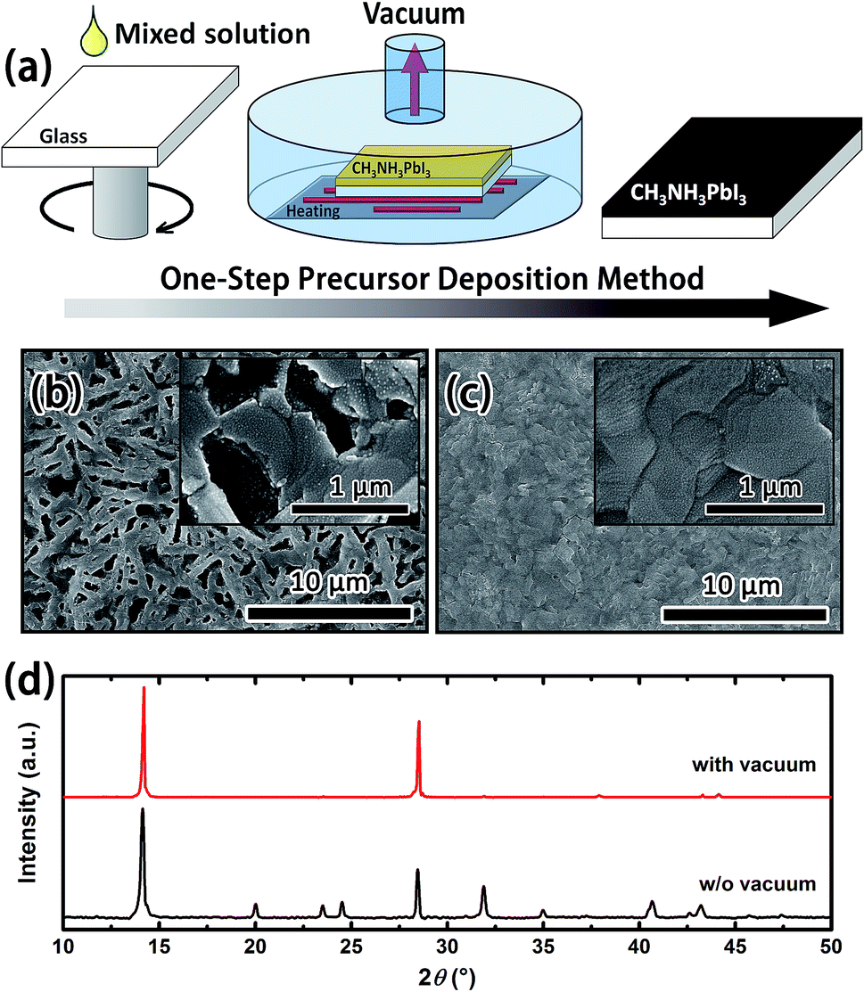 | ||
| Fig. 1 (a) Scheme of the vacuum-assisted deposition process. The SEM images of MAPbI3 films formed through annealing in N2 (b) and under vacuum-assistance (c). (d) The XRD patterns of MAPbI3 films annealed in N2 and vacuum. | ||
The morphology and crystallinity of the films treated under vacuum for different lengths of time were investigated by SEM images (Fig. S1†) and XRD patterns (Fig. S2†). The results indicate that more dense and smooth films were obtained by vacuuming for more than 10 min. The ASE performances of the corresponding films (Fig. S3†) were observed after vacuum-annealing with the setup shown in Fig. S4† and the lowest threshold was ∼40 μJ cm−2, which is a good result from perovskite based thin films.10,11 To further exhibit the optimization through vacuum-annealing, the ASE net gain and loss coefficients were studied and are shown in Fig. S5.† The increasing net gain and decreasing loss coefficients of each sample are summarized in Table S1,† which confirms the improved quality of the MAPbI3 films by the increase in vacuuming time.
As previously reported, the crystal structure of MAPbI3 can transform from the tetragonal phase to the orthorhombic phase with decreasing temperature.18 The temperature dependent phase transition can obviously affect the optical properties of MAPbI3 films. The PL spectra shown in Fig. S6† show that the temperature dependent mutation obviously occurred in the perovskite film with optimized morphology and crystallinity and was described as the temperature dependent phase transition.7 The above results demonstrate that vacuum-assisted annealing can eliminate pores and improve the crystallinity of perovskite thin films, enhancing the ASE performance and temperature dependent transition significantly. All the following investigations were based on the optimized MAPbI3 perovskite film with the morphology as shown in Fig. 1(c).
The temperature dependent XRD measurement was taken to provide direct evidence of the crystal structure phase transition, as shown in Fig. 2. The XRD diffraction peaks reveal good crystallinity and uniform orientation, which confirms the formation of the orthorhombic and the tetragonal perovskite structures.9,19 Above 150 K, the strong characteristic XRD peaks of the tetragonal phase at 14.126°, 23.521°, 28.463° and 31.895° were observed. At 150 K, another diffraction peak emerges at 32.895°. With a further decrease in temperature, strong characteristic peaks at 14.371°, 23.071°, 28.994° and 32.936° confirm that the crystal structure of perovskite film transitions to the orthorhombic structure.
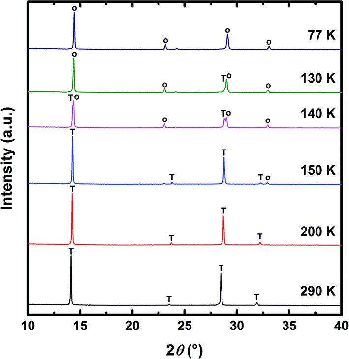 | ||
| Fig. 2 The XRD patterns of the optimized MAPbI3 perovskite film at various temperatures. T and O are XRD peaks from the tetragonal phase and orthorhombic phase respectively. | ||
To clearly investigate the change in crystal structure, we zoom in on the characteristic XRD peaks in Fig. S7(a)† and summarize the peak intensity and peak position in Fig. S7(b).† At the beginning of cooling, the change in the peak intensity and the peak position may come from the lattice contraction of MAPbI3. Around 150 K, the coexistence of the orthorhombic phase and the tetragonal phase inhibits the diffraction intensity and changes the XRD peak position abruptly, which is attributed to the random crystal orientation and distorted lattice structure. When the temperature continually decreases, the characteristic peaks of the tetragonal phase are hardly observed. Our XRD results clearly confirm the temperature dependent crystal structure transition between the tetragonal phase and the orthorhombic phase in the well crystalline MAPbI3 perovskite films.
Due to the temperature dependent phase transition, the optical absorption spectra of the optimized MAPbI3 perovskite film were closely related to the temperature, as shown in Fig. 3. The thin film exhibits ordinary absorption spectra above 270 K. A sharp shoulder at ∼770 nm emerges at lower temperatures, which is caused by an excitonic transition, and a second shoulder emerges at ∼740 nm below 150 K.20 With a further decrease in temperature, the latter shoulder (∼740 nm) gains strength in intensity and shifts to a longer wavelength while the first shoulder (∼770 nm) disappears, which can be attributed to the phase transition of the MAPbI3 thin films from a tetragonal phase to an orthorhombic phase, caused by continuous expansion and shrinkage of the lattice.21,22 The exciton binding energy (EB) can be calculated using the temperature-dependent absorption line width of the excitonic transition as described in ref. 20. By fitting the absorption data, we estimate an exciton binding energy of 45 ± 13 meV in the optimized MAPbI3 film, which is shown in Fig. S8.†
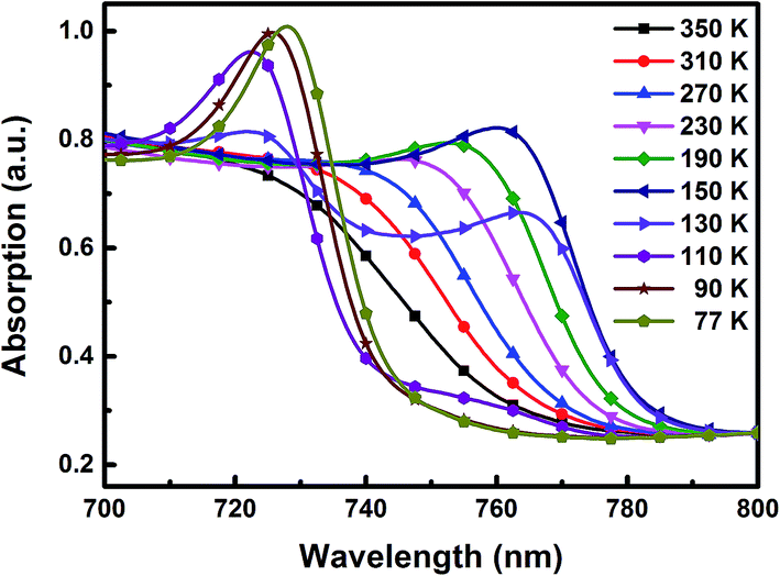 | ||
| Fig. 3 The absorption spectra of the optimized perovskite film at various temperatures (350–77 K). | ||
PL performances of the perovskite film during the phase transition are investigated and presented in Fig. 4. The deconvoluted Gaussian peaks of the PL emission band, illustrated by the colored curves at typical temperatures in Fig. 4(a), clearly show that the emission spectrum depends on temperature. The PL peak at room temperature (290 K), named peak 2, of the MAPbI3 perovskite film centers at ∼770 nm. With decreasing temperature, a red shift of peak 2 is observed. In the range of 130–10 K, the second PL peak, named peak 1, at a shorter wavelength arises and is enhanced. The temperature dependent PL spectra are mapped on the normalized false color image in Fig. 4(b), where the black dotted line and red dotted line mark the positions of the deconvoluted peaks of the PL spectra at different temperatures. In the range of 350–160 K, peak 2 shows a red shift and intensity increase with decreasing temperature, which is due to the reduction in the dissociation of free excitons and the change in material parameters contrasted to typical semiconductors.7,22 When further decreasing the temperature, an abnormal blue shift of peak 2 was observed in the range of 150 K to 100 K. Meanwhile, a new peak (peak 1) appears at ∼740 nm and the intensity gradually becomes strong, which is attributed to the phase transition from the tetragonal phase to the orthorhombic phase.9,18 Peak 1 and peak 2 are traced to the tetragonal phase and orthorhombic phase of MAPbI3, respectively. Furthermore, by reducing the temperature to 10 K, the central wavelength of the PL spectra and the intensity of peak 1 increased continually. The change of the PL peak positions is in accordance with the observation of the absorption edge of MAPbI3 at various temperatures (Fig. 3), which is a striking indication of the crystal structural phase transition.21
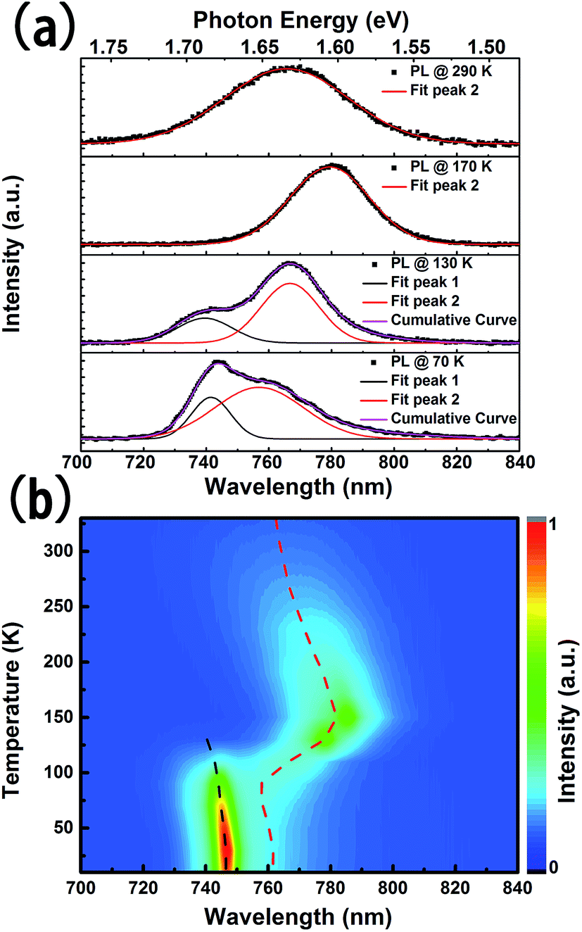 | ||
| Fig. 4 (a) The PL spectra and fitted peaks at typical temperatures of the optimized perovskite film. (b) The peak position is plotted as the dashed line in the image of the temperature dependent PL spectra in the temperature range from 350 K to 10 K. | ||
Based on the investigation of temperature dependent PL spectra, we know that the PL efficiency is enhanced with decreasing temperature, which is beneficial for lowering the ASE threshold.23 Fig. 5(a) presents the emission spectra of the perovskite thin film under 500 nm excitation with various pump intensities. Under low power excitation, only a broad spontaneous emission (SE) band can be observed at the ∼780 nm central wavelength. With gradually increasing pump intensity, the FWHM slowly decreases. When the pump intensity is above the threshold, ASEs for the orthorhombic phase and the tetragonal phase arise at about ∼770 nm and ∼740 nm, respectively. When the temperature is around 130 K, where the orthorhombic phase and the tetragonal phase coexist, ASE happens in the orthorhombic phase, although PL is more intense in the tetragonal phase.
 | ||
| Fig. 5 (a) The PL spectra of the MAPbI3 film at different excitation intensities and temperatures. (b) The output intensity as a function of pump intensity at different temperatures. (c) The temperature dependence of the PL peak position, ASE peak position and ASE threshold. | ||
To characterize the ASE performances at the different temperatures quantitatively, we calculated the ASE threshold for different temperatures. The dependence of output emission on pump intensity at the typical temperatures is shown in Fig. 5(b). From this figure, one can find that the ASE intensity is enhanced and the threshold is reduced by decreasing temperature. The threshold, which is ∼40 μJ cm−2 at room temperature, has reached its lowest, ∼10 μJ cm−2, around 50 K, which is roughly the same as the resonance induced ASE performance based on the perovskite materials excited by a femtosecond laser (∼100 fs).6,13 However, a non-monotonic rise of the threshold and abnormal peak shift are observed at about 130 K, which may come from the co-existence of the tetragonal phase and the orthorhombic phase. The messy crystal orientation leads to the increase in scatter in the film.10 The characters of SE and ASE at each temperatures are summarized in Fig. 5(c). Strikingly, the shift of the SE peaks with decreasing temperatures is in accordance with that of the PL spectra in Fig. 4(b). In this work, the position of the ASE peak was investigated. The ASE appears at the longer wavelength side of the PL peak above 130 K, and rises at the shorter wavelength side below 130 K, because of the narrower band gap of tetragonal MAPbI3.19,24 The increase in band gap results in the reduction in self-absorption at the shorter wavelength side.
To understand the abnormal increase of the ASE threshold and the ASE peak shifting, the mapping of time-resolved PL spectra at different temperatures was investigated in Fig. 6(a). From mapping, we find that the lifetime of the peak from the orthorhombic phase is shorter than that from the tetragonal phase. As is well known, the excited states with longer lifetimes will easily create population inversion, which benefits the ASE performance. Fig. 6(b) summarizes the temperature dependence and the lifetimes of the emissions from orthorhombic and tetragonal MAPbI3. Notably, the lifetimes of each PL peak all decrease to a lower level at ∼140 K, resulting from the dispersion of the carriers.9 The energy transfer and recombination processes in the coexisting phases can be supported by the Time-Resolved PL (TRPL) spectra shown in Fig. 6(c), where the dashed lines denote the shift of the emission peaks. From the TRPL spectra, peak 2 shifts to a longer wavelength with increasing delay time, which means that the carriers gradually migrate to a lower energy band after pulsed excitation. This red-shifted PL emission was attributed to a donor–acceptor pair (DAP) recombination.9 The photon energy and the recombination rate of the DAP emission are described by the following equations:
| ħω = Eg − EA − ED + e2/(4πε0εR) |
| 1/τDA ∝ exp[−2(R/αD,A)] |
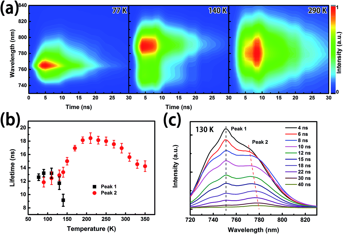 | ||
| Fig. 6 (a) Wavelength dependent PL lifetime mapping at 77 K, 140 K and 290 K. The effect of temperature on the lifetime of each PL peak (b) and the time resolution PL spectra as a function of time (c). | ||
Conclusions
In summary, vacuum-assisted annealing has been used in the fabrication of dense and smooth MAPbI3 films. The crystallinity and morphology are improved by increasing the vacuum time before annealing the films. The optimized sample exhibits excellent ASE performance and enhanced temperature dependent phase transition, which proves that the vacuum-assisted one-step precursor deposition method is an effective strategy for the fabrication of well-controlled morphology and crystallinity. The temperature dependent crystal structure phase transition was observed and proved by XRD patterns, absorption spectra and PL spectra with decreasing temperature. In addition, we have also demonstrated the ASE performance during the phase transition. The ASE performance was well-enhanced by decreasing the temperature and influenced by the phase transition. Our results, showing enhanced ASE performance with the lowest threshold of ∼40 μJ cm−2 at room temperature and ∼10 μJ cm−2 at about 50 K, clearly indicate that the vacuum-assisted precursor deposition method can enhance the temperature dependent optical characteristics, and provides an excellent pathway for achieving high-performance and cost-effective perovskite-based coherent light source devices that can be implemented in the near future.Experimental section
Sample preparation
Condense and pore-free perovskite films were prepared via a vacuum-assisted thermal treatment. The mixture of PbI2 (99%, Alfa Aesar) and MAI (99%, Dyesol) in a stoichiometric ratio was dissolved in DMSO (99.8%, Alfa Aesar) with a concentration of 0.8 M and stirred at 70 °C overnight in a nitrogen filled glove box, and cooled down to 50 °C before spin-coating. The perovskite layer was then deposited by spin coating the precursor solutions directly on the glass substrates at 3000 rpm for 50 s. After spin coating, the films were immediately vacuumed in a chamber for 0, 5, 10 min and more without annealing. Then the perovskite films with a typical thickness of 350 nm were obtained by heating the films to 90 °C slowly (∼1.5 °C min−1) and keeping for 4 h under vacuum.Film characterization
A field emission scanning electron microscope (FE-SEM, Hitachi-S4800) was used to obtain SEM images. The room temperature X-ray diffraction (XRD) patterns were recorded by a Bruker D8 Advance X-ray diffractometer. The temperature dependent XRD patterns were measured by a Bruker D8 Discover X-ray diffractometer with non-ambient stages. The thicknesses of the films were measured by an Ambios Technology XP-2 surface profilometer. The temperature dependent Ultraviolet-Visible (UV-vis) absorption spectra were collected by a Shimadzu UV-3101PC spectrometer with a Microscopy Cryostat System (Cryo Industries of America). A Continuum SureLite II Nd3+: YAG laser pumping a Continuum SureLite optical parametric oscillator (OPO) was employed as the excitation source for ASE and TRPL measurements of the perovskite films. The laser pulse energy was detected with a Coherent J-10SI-HE power meter. The temperature dependent ASE emission spectra were recorded using an Acton-150 imaging spectrophotometer with a Helium Cryostat System (Oxford Optistat, CCC1104). The temperature dependent PL spectra were collected by a spectrometer (Horriba, iHR320). The TRPL spectra were acquired by a spectrometer (Jobin Yvon Triax 320). The schematic of the optical measurement setup is shown in Fig. S4.†Acknowledgements
This research is supported by the Natural Science Foundation of China (Grant No. 61475017, 61275175, 61377028, 61475014, 61675018, 61674012 and 51603010), and the Fundamental Research Funds for the Central University (2014JBZ009).Notes and references
- W. S. Yang, J. H. Noh, N. J. Jeon, Y. C. Kim, S. Ryu, J. Seo and S. I. Seok, Science, 2015, 348, 1234–1237 CrossRef CAS PubMed.
- H. Cho, S.-H. Jeong, M.-H. Park, Y.-H. Kim, C. Wolf, C.-L. Lee, J. H. Heo, A. Sadhanala, N. Myoung, S. Yoo, S. H. Im, R. H. Friend and T.-W. Lee, Science, 2015, 350, 1222–1225 CrossRef CAS PubMed.
- L. Dou, Y. M. Yang, J. You, Z. Hong, W. H. Chang, G. Li and Y. Yang, Nat. Commun., 2014, 5, 5404 CrossRef CAS PubMed.
- F. Deschler, M. Price, S. Pathak, L. E. Klintberg, D. D. Jarausch, R. Higler, S. Huttner, T. Leijtens, S. D. Stranks, H. J. Snaith, M. Atature, R. T. Phillips and R. H. Friend, J. Phys. Chem. Lett., 2014, 5, 1421–1426 CrossRef CAS PubMed.
- G. Xing, N. Mathews, S. Sun, S. S. Lim, Y. M. Lam, M. Gratzel, S. Mhaisalkar and T. C. Sum, Science, 2013, 342, 344–347 CrossRef CAS PubMed.
- S. D. Stranks, S. M. Wood, K. Wojciechowski, F. Deschler, M. Saliba, H. Khandelwal, J. B. Patel, S. J. Elston, L. M. Herz, M. B. Johnston, A. P. H. J. Schenning, M. G. Debije, M. K. Riede, S. M. Morris and H. J. Snaith, Nano Lett., 2015, 15, 4935–4941 CrossRef CAS PubMed.
- K. Wu, A. Bera, C. Ma, Y. Du, Y. Yang, L. Li and T. Wu, Phys. Chem. Chem. Phys., 2014, 16, 22476–22481 RSC.
- X. Y. Chin, D. Cortecchia, J. Yin, A. Bruno and C. Soci, Nat. Commun., 2015, 6, 7383 CrossRef CAS PubMed.
- W. Kong, Z. Ye, Z. Qi, B. Zhang, M. Wang, A. Rahimi-Iman and H. Wu, Phys. Chem. Chem. Phys., 2015, 17, 16405–16411 RSC.
- T. S. Kao, Y.-H. Chou, C.-H. Chou, F.-C. Chen and T.-C. Lu, Appl. Phys. Lett., 2014, 105, 231108 CrossRef.
- G. Xing, N. Mathews, S. S. Lim, N. Yantara, X. Liu, D. Sabba, M. Gratzel, S. Mhaisalkar and T. C. Sum, Nat. Mater., 2014, 13, 476–480 CrossRef CAS PubMed.
- H. Zhu, Y. Fu, F. Meng, X. Wu, Z. Gong, Q. Ding, M. V. Gustafsson, M. T. Trinh, S. Jin and X. Y. Zhu, Nat. Mater., 2015, 14, 636–642 CrossRef CAS PubMed.
- Q. Zhang, S. T. Ha, X. Liu, T. C. Sum and Q. Xiong, Nano Lett., 2014, 14, 5995–6001 CrossRef CAS PubMed.
- L. Qin, L. Lv, Y. Ning, C. Li, Q. Lu, L. Zhu, Y. Hu, Z. Lou, F. Teng and Y. Hou, RSC Adv., 2015, 5, 103674–103679 RSC.
- Y. Yasuhiro, N. Toru, E. Masaru, W. Atsushi and K. Yoshihiko, Appl. Phys. Express, 2014, 7, 032302 CrossRef.
- Z. Xiao, Q. Dong, C. Bi, Y. Shao, Y. Yuan and J. Huang, Adv. Mater., 2014, 26, 6503–6509 CrossRef CAS PubMed.
- M. Nishimura, M. Nakayama and T. Yano, J. Chem. Eng. Jpn., 1972, 5, 223–226 CrossRef CAS.
- A. Poglitsch and D. Weber, J. Chem. Phys., 1987, 87, 6373 CrossRef CAS.
- T. Baikie, Y. Fang, J. M. Kadro, M. Schreyer, F. Wei, S. G. Mhaisalkar, M. Graetzel and T. J. White, J. Mater. Chem. A, 2013, 1, 5628–5641 CAS.
- V. D’Innocenzo, G. Grancini, M. J. Alcocer, A. R. Kandada, S. D. Stranks, M. M. Lee, G. Lanzani, H. J. Snaith and A. Petrozza, Nat. Commun., 2014, 5, 3586 Search PubMed.
- T. Ishihara, J. Lumin., 1994, 60, 269–274 CrossRef.
- Y. P. Varshni, Physica, 1967, 34, 149–154 CrossRef CAS.
- R. Gupta, J. Park, V. Srdanov and A. Heeger, Synth. Met., 2002, 132, 105–107 CrossRef CAS.
- Y. Wang, T. Gould, J. F. Dobson, H. Zhang, H. Yang, X. Yao and H. Zhao, Phys. Chem. Chem. Phys., 2014, 16, 1424–1429 RSC.
Footnote |
| † Electronic supplementary information (ESI) available: SEM, XRD patterns, ASE performance and TRPL spectra. See DOI: 10.1039/c7ra01155e |
| This journal is © The Royal Society of Chemistry 2017 |