
 Open Access Article
 This Open Access Article is licensed under a Creative Commons Attribution-Non Commercial 3.0 Unported Licence
Direct assembly of thioacid capped quantum dots in solid-state hybrid photovoltaics, effect of QDs size and thermal annealing†
Manuel A. Triana *a,
Oscar A. Jaramillo-Quinterob,
Rubén J. Camargoa and
Marina E. Rincónb
*a,
Oscar A. Jaramillo-Quinterob,
Rubén J. Camargoa and
Marina E. Rincónb
aEscuela de Ingeniería Química, Universidad del Valle, Ciudad Universitaria Meléndez, A. A. 25360, Cali, Colombia. E-mail: manuel.triana@correounivalle.edu.co
bInstituto de Energías Renovables, Universidad Nacional Autónoma de México, Privada Xochicalco S/N, C.P. 62580 Temixco, Mor., Mexico
First published on 28th February 2017
Abstract
Deposition of colloidal quantum dot thin films to fabricate hybrid solar cells is strongly dependent on the nature of the quantum dot (QD) surface ligand. In order to reduce the fabrication cost and eliminate additional steps as the ligand-exchange, water soluble quantum dots (WSQDs) can be directly assembled in solid-state hybrid photovoltaics. In this paper we present the synthesis and characterization of solution processed quantum dot solar cells (QDSCs) with mercaptosuccinic acid (MSA) capped CdSe QDs as the active layer, rutile TiO2 nanorods (NRs) as the electron transport material (ETM) and Spiro-OMeTAD as the hole transport material (HTM). Narrow size distribution and surface coordination of the WSQDs were critical on the performance of the devices, with 3.5 nm CdSe QDs yielding the best power conversion efficiency (PCE). Annealing of the CdSe QD layer at 190 °C and room temperature infiltration of Spiro-OMeTAD into the active layer, simultaneously increased Voc, Jsc, and PCE. Proper annealing increases the QD size and removes linked water and excess ligands, contributing to QD packing and better electron-transport through the active layer. The improvement of Voc observed after further HTM infiltration, can be ascribed to the surface passivation of in-gap trap states and weak p-doping of QDs induced by 4-tert-butylpyridine, as evidenced by Kelvin probe measurements.
Introduction
Solution-processed quantum dot solar cells (QDSCs) continue to be one of the most suitable candidates for 3rd generation solar devices.1,2 In order to promote the use of low-cost green materials, hybrid composites of inorganic QDs/π conjugated polymers are being the subject of extensive research for photovoltaic applications.3–5 In this sense, water soluble quantum dots (WSQDs) are a good alternative to replace organometallic synthesized quantum dots (ORQDs) in solid-state solar cells. The organometallic synthesis of CdSe QDs has been reported to be about 8 times more expensive than the aqueous route.6 Employing high quality WSQDs eliminates the use of organic solvents and high temperatures during the synthesis. In addition, since WSQDs have very short ligands, ligand exchange7 to replace the native long ligands from ORQDs may be avoided.Conventional deposition techniques to assemble hybrid devices based on WSQDs are inappropriate, due to the low volatility and large surface tension of water as a solvent. Subsequently, alternative techniques have been used to assemble WSQDs of CdSe, CdS, CdTe, HgTe, in solid-state hybrid devices. The most common techniques are electrostatic layer-by-layer (ELBL) deposition by dip-coating7–9 and spray-coating.10,11 ELBL deposition consists of alternating self-assembly of QD monolayers and polyelectrolyte layers, which results in a very stable film but with a high energy barrier for charge transfer due to the presence of the cross-linkers (polyelectrolytes).9 The poly-ion also constitutes the p-type material in some devices.7 For deposition of thin layers (30–200 nm) and assembly of optoelectronic devices, such as LEDs10 and photodetectors,11 spray-coating of WSQDs has been ideal although it requires complex drying control to have good reproducibility. More recently, spin-coating was successfully used to deposit CdTe QDs stabilized in water with 2-mercaptoethylamine (MA) over a TiO2 compact layer.12 Opposite to the high repulsion experienced between thioacid capped QDs, this thiol–amine allows higher concentration of QDs in water, and the amine can easily anchor to the TiO2 surface by means of hydrogen bonds.
Another big challenge in solid-state hybrid solar cells using QDs is the charge transfer improvement at the QD surface. In particular, efficient charge transfer at the interface n-type QD/hole transport material (HTM) is required, due to low carrier mobility in QDs compared to the bulk material. Hence, hetero-interfacial contact between QDs and the HTM can be improved, through pore infiltration of the HTM into the active layer and removal of the capping agent at the QD's surface. Different conjugated polymers have been used as solid HTMs in hybrid photovoltaics with CdSe QDs, e.g., poly(9,9-dioctylfluorene-co-N-(4-utylphenyl)diphenylamine (TFB),9 poly(1-methoxy-4-(2-ethylhexyloxy-2,5-phenylenevinylene)) (MEH-PPV),13 poly(3-hexylthiophene) (P3HT)13,14 and poly[2,6-(4,4-bis(2-ethylhexyl)-4H-cyclopenta[2,1-b;3,4-b′]-dithiophene)-alt-4,7-(2,1,3-benzothiadiazole)] (PCPDTBT).15,16 Currently, the inverted QD-polymer solar cells has the highest power conversion efficiency (PCE), 3.0–4.2%,15–17 of the spherical CdSe QD based devices. For this configuration the active layer is frequently a QD/polymer blend, where the donor material is a low band-gap polymer (p-type) and the acceptor material is an interconnected network of spherical CdSe nanocrystals (NCs). However, for these solar cells the CdSe QDs are still synthesized by the organometallic route and need post-synthetic surface modification.
In this contribution, the synthesis and characterization of hybrid QDSCs with configuration: FTO/TiO2 NRs/CdSe QDs/Spiro-OMeTAD/Au is presented. CdSe QDs were synthesized by the aqueous route, using mercaptosuccinic acid (MSA) as the stabilizing agent. A modified drop-coating technique was implemented to directly deposit the QDs on top of rutile TiO2 nanorods (NRs). 2,2′,7,7′-tetrakis (N,N′-di-p-methoxyphenylamine)-9,9′-spirobifluorene (Spiro-OMeTAD) was used as HTM due to its low molecular weight and high pore filling.18,19 The effect of the QDs size and thermal annealing of the devices, before and after Spiro-OMeTAD deposition, on the solar cell performance is discussed. The best solar cell doubled the PCE previously reported for solid-state hybrid devices with colloidal CdSe QDs synthesized by aqueous route.9 Direct deposition means that nor ligand exchange neither cross-linkers were used for QD deposition, to avoid higher cost and larger energy barriers in the active layer, respectively. The devices herein presented are QD-based solar cells even after annealing of the active layer, since the growth of CdSe nanocrystals remains in the regime of quantum confinement.
Results and discussion
Aqueous synthesis of MSA capped CdSe QDs
The CdSe QDs were synthesized by modifying a method previously reported.20 First, nucleation of CdSe nanocrystals capped with MSA was carried out inside a glove box filled with N2. Conventional growth of water-soluble nanocrystals is usually inside a reflux system, limited by the boiling temperature of water under atmospheric pressure. Therefore, in order to increase the boiling temperature and consequently the growth rate of the nanocrystals, the raw solution was heated inside an autoclave (under P > Patm). Different raw solutions were subjected to growth periods of 2, 3 and 4 h at 135 °C, henceforth the QDs grown for these periods are referenced as: QDs-2 h, QDs-3 h and QDs-4 h, respectively. The detailed procedure for synthesis and growth of the nanocrystals can be found in the Experimental section.Optical and morphological characterization of CdSe QDs
Fig. 1 shows the absorption and photoluminescence (PL) spectra of the QD solutions measured after hydrothermal growth. All solutions have well defined excitonic absorption peaks as can be observed in Fig. 1a. Optical band gap energies (Eopg) of the QDs obtained from the UV-vis spectra and Tauc's graphical method22 are presented in Table 1. On the other hand, Fig. 1b shows narrow emission peaks corresponding to QDs grown during 3 and 4 h, with full width at half maximum (FWHM) ≤ 31 nm (see Table 1). This indicates good size refinement controlled by the stabilizing agent (MSA). Among different thioacid agents, MSA has shown to be an excellent surfactant evidenced by strong reduction of non-radiative recombination in the QDs. The absolute PL spectra of equally diluted QD solutions, reveals a growth period of 3 h as the brightpoint,17 transition from nuclei growth stage to Ostwald-ripening21 is observed afterwards. Inset in Fig. 1b shows a color red-shift (left-right) in emission of the QD solutions under UV radiation.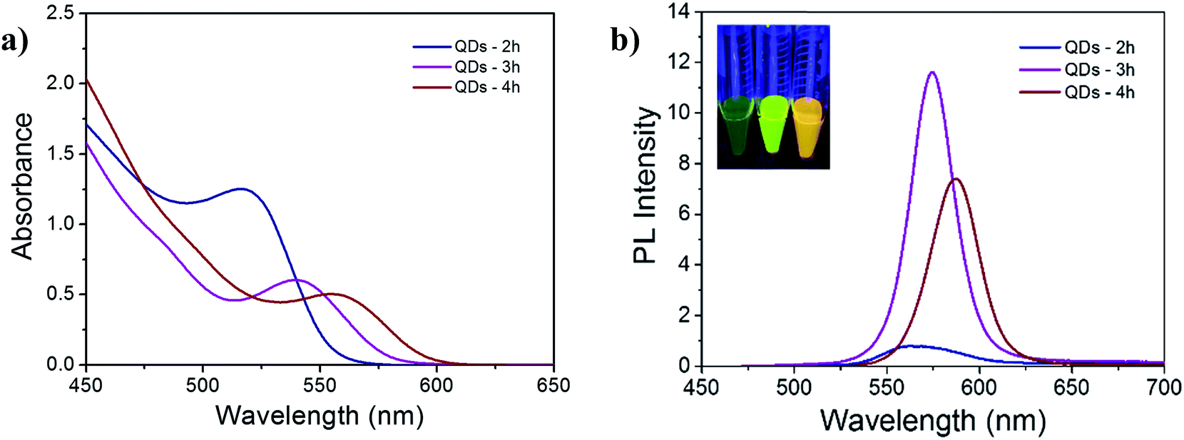 | ||
| Fig. 1 (a) Absorption and (b) photoluminescence spectra of the CdSe QDs in aqueous solution, grown during 2, 3 and 4 h at 135 °C (excitation wavelength: 365 nm). The inset shows solutions of QDs grown for 2, 3 and 4 h (left to right) under UV radiation (365 nm). | ||
| Growth period (h) | 1st excitonic absorption peak λ (nm) | Diameter – TEM (nm) | FWHM – TEM (nm) | FWHM – PL width in λ (nm) | Eopg (eV) Tauc |
|---|---|---|---|---|---|
| 2 | 516.5 | 2.75 ± 0.01 | 0.69 ± 0.04 | 49 | 2.3 |
| 3 | 539.5 | 3.49 ± 0.01 | 0.52 ± 0.04 | 27 | 2.2 |
| 4 | 554.5 | 4.07 ± 0.01 | 0.66 ± 0.03 | 31 | 2.1 |
Morphological characterization using transmission electronic microscopy (TEM) was also carried out to find the average diameter and particle size distribution (PSD) of the QDs. TEM images (Fig. 2) show good monodispersity of the QDs and PSDs of Fig. S1† (from the ESI†) are narrow. The average size and FWHM based on TEM are also summarized in Table 1, with the respective standard deviation. As expected, the narrowest PSD from TEM and the minimum FWHM calculated from the PL spectra corresponded to QDs-3 h, and the nanocrystals grown during 4 h presented the largest diameter and the lowest band gap energy.
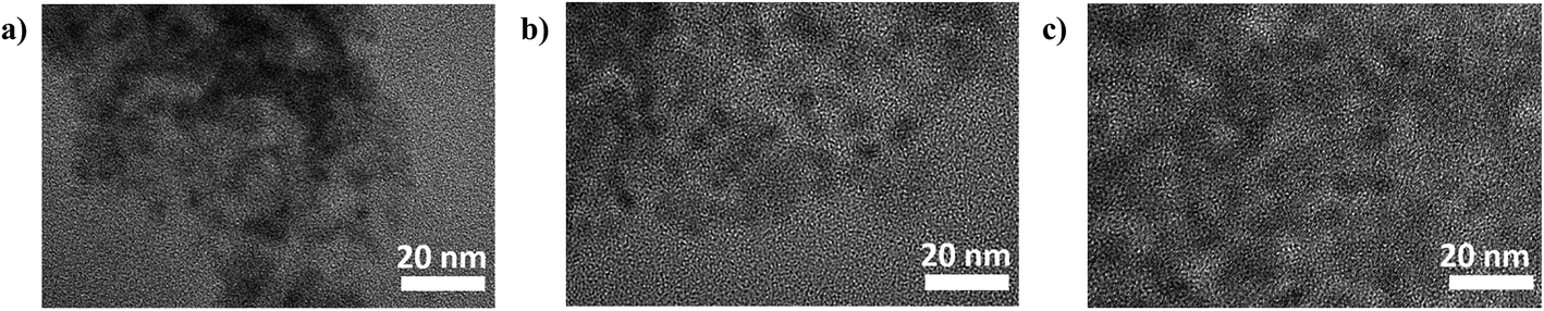 | ||
| Fig. 2 TEM images of the CdSe (a) QDs-2 h, (b) QDs-3 h and (c) QDs-4 h. | ||
Deposition of CdSe QDs films on top of rutile TiO2 NRs
In order to increase the hetero-interfacial area between the electron transport material (ETM) and CdSe QDs, TiO2 NRs were used instead of a compact thin layer. The TiO2 NRs were directly grown on fluorine-tin oxide (FTO) substrates by hydrothermal route, following a procedure published elsewhere.23,24 This method results in TiO2 NRs with rutile phase, and average nanorod length of 600 nm corresponding to 1.5 h of hydrothermal growth inside an autoclave. These properties were evidenced through the XRD pattern of Fig. S2† and SEM image of Fig. S3.† For reaction times less than 1.5 h the NR films were not homogeneous. Subsequently, the NRs surface was subjected to a second hydrothermal treatment to avoid short-circuit and reduce electron recombination through trap-states.Two different techniques were evaluated in order to find the best deposition of CdSe QDs layers on top of TiO2 NRs. CdSe QDs deposition by a spray-coating was first assayed following conditions previously reported.11 A substrate with TiO2 NRs was placed over a hot-plate and kept at 45 °C, then, an amount of CdSe QD solution was spread on top of the TiO2 NRs surface using an airbrush with nozzle of 0.3 μm and 40 spray applications. The key for this technique lays on the time interval between applications. If it is long just tiny spots are formed and disappear in subsequent spraying. Otherwise, if it is short a thicker liquid layer is deposited and only one – large – spot is formed after drying (see Fig. S4a, ESI†). For the last case, the usual coffee-ring effect was not observed, since dense deposition was experienced at inner areas instead of at the perimeter. In fact, controlling the homogeneous deposition of CdSe QDs was very difficult.
In order to simplify the deposition technique, frame assisted thermal drop-coating was a good alternative. Although normal drop-coating still resulted in spots at inner areas, homogeneous CdSe QD layers were obtained by using a frame of copper wire around the deposition area. The substrate with TiO2 NRs was first fastened over a metal sheet with copper wire (as shown in Fig. S4b, ESI†), the assembly was placed over a hot plate and kept at 47 °C, then the QD solution was dripped and distributed inside the limited area. After just 15 minutes a dried layer was achieved with small accumulation at the border limited by the frame, but with homogeneous deposition at the inner area. The coffee-ring was well controlled by driving the capillary flow to the edge of the substrate. Neutral pH of the QD solution (∼7.5) allowed interfacial affinity between TiO2 NRs and MSA capped CdSe QDs (see Fig. 3a), aiding to the wetting of the whole surface. One key to obtain homogeneous deposition was the complete wetting of the frame, Fig. 3b illustrates the thermal deposition and the meniscus formed over the wire due to the large surface tension of water. Finally, the high porosity of the TiO2 NRs films increased the adsorption of the nanocrystals and the thermal treatment improved the diffusion rate and ordering of the nanocrystals through the interstitial matrix of the NRs.
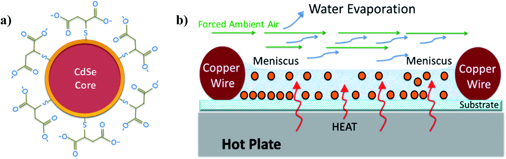 | ||
| Fig. 3 (a) Schematic illustration of a MSA capped CdSe QD, stabilized in water through dissociation of carboxylic acids into carboxylates. (b) Sectional sketch of the CdSe QD layer deposition by frame assisted thermal drop-coating. | ||
Once the drop-coating conditions were stablished, the maximum thickness of the QD layer was determined by the maximum concentration allowed for the initial QD solution. For the MSA capped CdSe QDs, saturation in water solution under room conditions was usually around 13.6 mg mL−1. However, the concentration for deposition must be lower, around 10 mg mL−1, due to the drying dynamics. When the dripped solution was above 10 mg mL−1, the solution reached saturation before total evaporation of water. Visible agglomeration of the nanocrystals across the surface evidenced drying under saturation condition. The average thickness of the CdSe QD over-layer deposited with 10 mg mL−1 solution was 96 nm, measured with field emission scanning electron microscopy (FESEM). Fig. 4a shows a SEM image of the cross-section, where infiltration of the CdSe QDs between the NRs can be observed, and the over-layer is highlighted in light orange (eye guideline). The baseline to calculate the over-layer was placed over the upper tip of TiO2 NRs, Fig. 4b shows a zoom of the cross section where the upper tips are clearly visible.
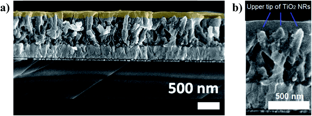 | ||
| Fig. 4 (a) Cross-sectional SEM micrograph of CdSe QD layer deposited by thermal drop-coating on top of the TiO2 NRs. (b) Zoom of the cross section to identify the upper tip of TiO2 NRs. | ||
Concentrations of the CdSe QD solution below 10 mg mL−1 were also used for deposition, 6 and 7.5 mg mL−1, but the respective thinner layers led to reduction on the photovoltaic performance of the devices.
Effect of QDs size and annealing treatment on the solar cells performance
Fig. 5a shows the J/V curves of the QDSCs based on CdSe QDs grown for 2, 3, and 4 h, labeled as: QDSC-A 2 h, QDSC-A 3 h and QDSC-A 4 h, respectively. –A means CdSe layer annealed after deposition, and only the non-annealed device with QDs-3 h is presented to observe the annealing effect (QDSC 3 h). The electronic band gap coupling and the active layer porosity were considered as the main size-dependent properties affecting the assembly and photovoltaic performance. First, effective charge transfer at the interfaces must be guaranteed by proper energy level alignment as the QD size changes. For the size range of the CdSe QDs evaluated the conduction band edge energy (CBM) changes quickly with the QD size, meanwhile the valence band edge energy (VBM) does not change significantly respect to the bulk VBM.25 Therefore, variation of the QD size mainly modifies the driving force for electron injection at the interface CdSe QDs/TiO2 NRs, and also the visible light absorption. An increase of both driving force and light absorption leads to an increment of the photo-generated current; however these phenomena change inversely along with variation of the QD size.26 In this sense, an optimum QD size corresponding to maximum photocurrent can be found in a size range limited by two conditions: zero electron injection (largest size) and poor visible light absorption (smallest size). For the present case, an optimum was found (QDs-3 h) in the size range evaluated, although this optimum is influenced by morphological and surface effects. As shown in Table 2, the best short circuit current density (Jsc) of 0.22 mA cm−2 was obtained after annealing the CdSe film with QDs-3 h. Annealing at 190 °C causes a red-shift of the excitonic peak (35 nm), indicating in situ growth of the QDs (Fig. 5b). By using the Tauc's graphical method, an optical band gap energy of 2.06 eV was calculated after annealing. When comparing with the Eopg of 3.5 nm QDs (2.2 eV, see Table 1) and the bulk band gap energy of the CdSe (1.74 eV), it can be inferred that the slightly grown CdSe nanocrystals are still under quantum confinement. The energy level scheme of the solar cells QDSC 3 h and QDSC-A 3 h shows proper band alignment for charge transfer, as depicted in Fig. 5c. All values are indexed to the vacuum energy,27,28 and the band edge energies (CBM and VBM) of the CdSe QDs were calculated using semi-empirical equations.29 More effective use of photon energy could be achieved with a well-defined range of QD sizes in the same device, but cascaded energy alignment is needed. In a cascaded-junction QD solar cell, the loss of electron kinetic energy and extracted electrochemical potential is reduced by selective photon absorption.30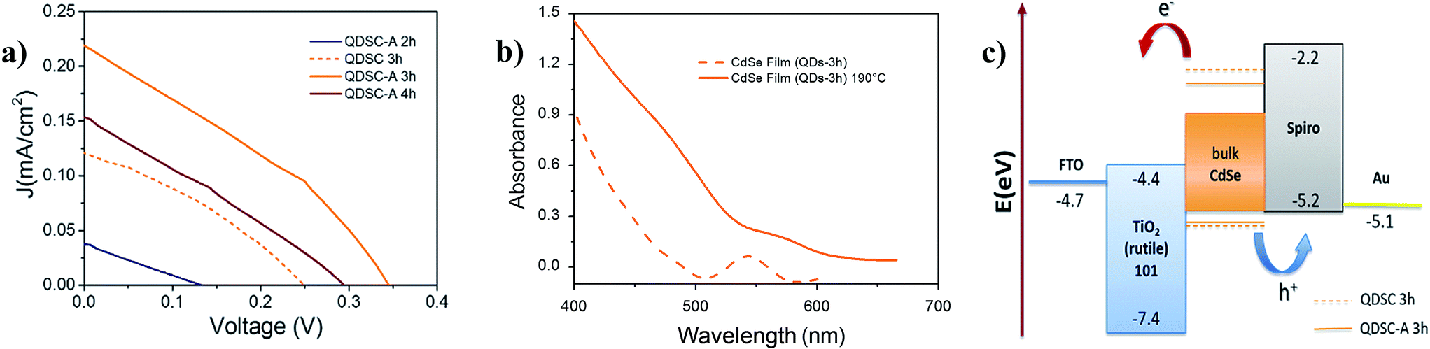 | ||
| Fig. 5 (a) J/V curves of annealed devices with QDs-2 h, QDs-3 h and QDs-4 h (annealing before HTM deposition), and non-annealed device with QDs-3 h. Under AM1.5G 100 mW cm−2 illumination. (b) Optical absorbance spectra of CdSe films with QDs-3 h: non-annealed and annealed at 190 °C, respectively. (c) Energy level scheme of the solar cells QDSC 3 h and QDSC-A 3 h, respectively. | ||
| Jsc (mA cm−2) | Voc (V) | FF | PCE (%) | |
|---|---|---|---|---|
| QDSC-A 2 h | 0.04 ± 0.008 | 0.13 ± 0.0003 | 0.24 ± 0.004 | 0.001 ± 0.0003 |
| QDSC 3 h | 0.12 ± 0.02 | 0.25 ± 0.0003 | 0.33 ± 0.002 | 0.010 ± 0.002 |
| QDSC-A 3 h | 0.22 ± 0.04 | 0.34 ± 0.0003 | 0.37 ± 0.001 | 0.028 ± 0.005 |
| QDSC-A 4 h | 0.16 ± 0.03 | 0.29 ± 0.0003 | 0.29 ± 0.001 | 0.014 ± 0.003 |
Incident photon to current efficiency (IPCE) measurements were also carried out to compare the annealed solar cells. The IPCE spectra shown in Fig. S5, of the ESI,† indicate that the QDSC-A 3 h yields the highest external quantum efficiency (EQE), with a maximum of 6% at 460 nm, in contrast with a maximum EQE of 2.2% at 390 nm reported for thioglycolic acid (TGA) capped CdSe QDs.9 This result is consistent with the reduction of carrier recombination and maximum Jsc found for QDs-3 h, after annealing. The trend of the EQE increase for different sizes is equally consistent with the J/V curves of Fig. 5a, and the onset of the IPCE spectra matches with the onset of the absorption spectra in Fig. 1a.
While the electronic band alignment directly affects the Jsc, the morphological effect is assumed to mainly influence the Voc. As the QD size increases, the QD layer porosity also increases. In consequence, larger hetero-interfacial area between the QDs and the HTM are expected under higher infiltration of the Spiro-OMeTAD at larger QD size. One proof of higher pore filling at larger QD size is the substantial reduction of the series resistance (Rs) observed when comparing the QDSC-A 2 h and QDSC-A 3 h devices (Table S1, ESI†). An 80% reduction of the Rs can be ascribed for the most part to better hetero-interfacial contact and QD surface passivation (discussed later). Moreover, the important increment of Voc observed in larger QDs (see Table 2) suggests the removal of in-gap trap states in these QDs. In addition, from Table S1† a size dependence of the shunt resistance (Rsh) can be inferred. Since larger QDs yielded lower Rsh, higher porosity (i.e. higher infiltration of the HTM) may lead to irregular deposition of the top-layer by spin-coating. On this basis, achieving an optimum HTM loading by using lower spin-rates could reduce the leakage current associated with physical defects and low Rsh.
Surface coordination and size distribution can be correlated to the growth kinetics of QDs, affecting both the trap-states surface density and the energy alignment. From the PL spectra (Fig. 1b), the QDs-2 h show the widest FWHM (49 nm) and lowest PL intensity. Low photoluminescence is the result of poor surface coordination which lead to trap-assisted non-radiative recombination. Moreover, although both QDs-3 h and QDs-4 h showed a narrow size distribution, the maximum photoluminescence quantum yield (PLQY%) makes the difference. Therefore, since the QDs-3 h yielded the highest PLQY (∼11% respect to rhodamine 6G), this suggest a better coordination of Cd atoms and fewer trap-states at the QD surface, leading to recombination reduction for charge transfer.
In order to evaluate the annealing effect on the composition of the CdSe QD layers, infrared (IR) spectra by attenuated total reflectance (ATR) were obtained for non-annealed and annealed films. In Fig. 6a, broad absorption band around 2750–3600 cm−1 observed in the non-annealed prototype almost disappeared after thermal annealing (red curve). –OH stretching vibrations corresponding to linked water and carboxylic acids (–COOH) are located at this region. C–H stretching vibrations found between 2800 and 3000 cm−1, characteristic of alkyl chains, are usually overlapped by the –OH acid contribution. Removal of excess ligands and water – accumulated or weakly linked, contributes to better contact between the HTM blend and the core surface of the QDs, explaining the 37% reduction of Rs and the increment on Voc (from 0.25 to 0.34 V) after annealing.
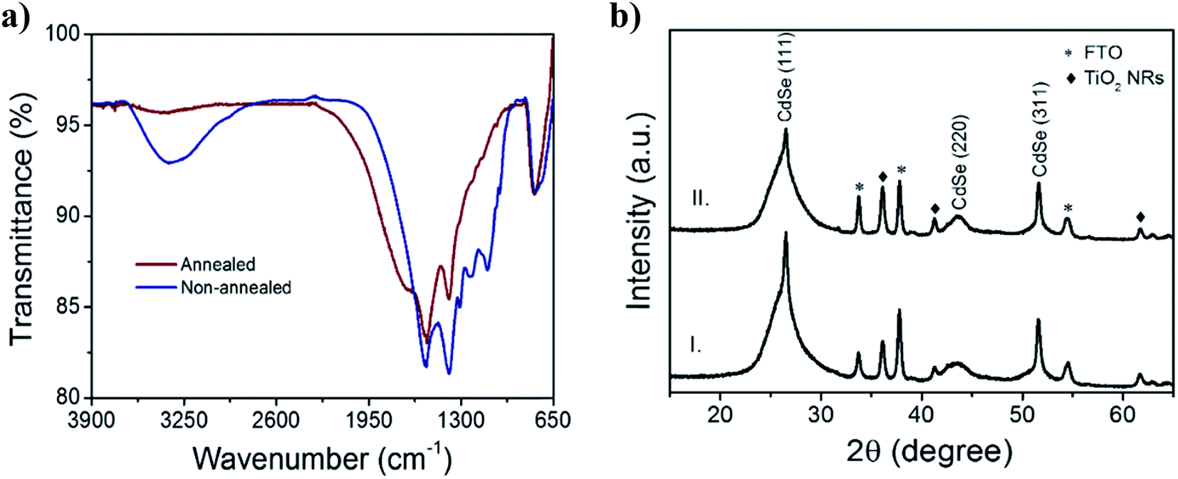 | ||
| Fig. 6 (a) FTIR spectra of: non-annealed CdSe QD layer (blue curve); CdSe QD layer annealed at 190 °C (red curve). (b) XRD pattern of: (I) non-annealed CdSe QD layer; (II) CdSe QD layer annealed at 190 °C. | ||
Aiming to demonstrate that the photocurrent improvement after annealing (see Fig. 5a) is caused by a dense packing of QDs, instead of crystalline phase transition, X-ray patterns of the CdSe QD films were measured. All the diffraction peaks can be assigned to zinc blende structure, similar to CdSe QDs synthesized at low temperature.20 The characteristic peaks of zinc blende were found at 2θ: 26.5°, 43.5° and 51.6° corresponding to planes (111), (220) and (311), respectively. Other diffraction peaks can be indexed as the tetragonal rutile phase of TiO2 and FTO (see Fig. S2†). Based on the literature,20 transition temperature between zinc blende and wurtzite structure is around 200 °C, and the annealing temperature (190 °C) was closed to this limit. However, the annealed CdSe QD layers kept the zinc blende structure, as shown in Fig. 6b.
Evaluation of the HTM (Spiro-OMeTAD) and pore filling effect
Herein, pore filling was considered in devices with QDs-3 h under two different temperatures and periods: (1) assembled devices were kept at room temperature (∼25 °C) for 1 week. (2) After Spiro-OMeTAD deposition, the devices were annealed at 190 °C for 1 h on a hot plate. In both cases the devices were inside a glovebox with N2, to avoid over-oxidation and consequent loss of conductivity of the Spiro-OMeTAD.The photovoltaic performance and J/V parameters of fresh (1 day) and aged (1 week) devices can be observed in Fig. 7 and Table 3, respectively. After 1 week, the PCE of the QDSCs increased from 0.028 to 0.045% with a simultaneous increase in Voc, Jsc and the fill factor (FF), as in previous report.31 It is noticeable the significant increase in Voc compared to the other parameters. This result suggests that during 1 week of aging, further infiltration of Spiro-OMeTAD took place from the over-layer into the pores of the CdSe QD layer. Under N2 atmosphere, the Voc increase is not attributable to HOMO level change of the Spiro-OMeTAD by oxidation.
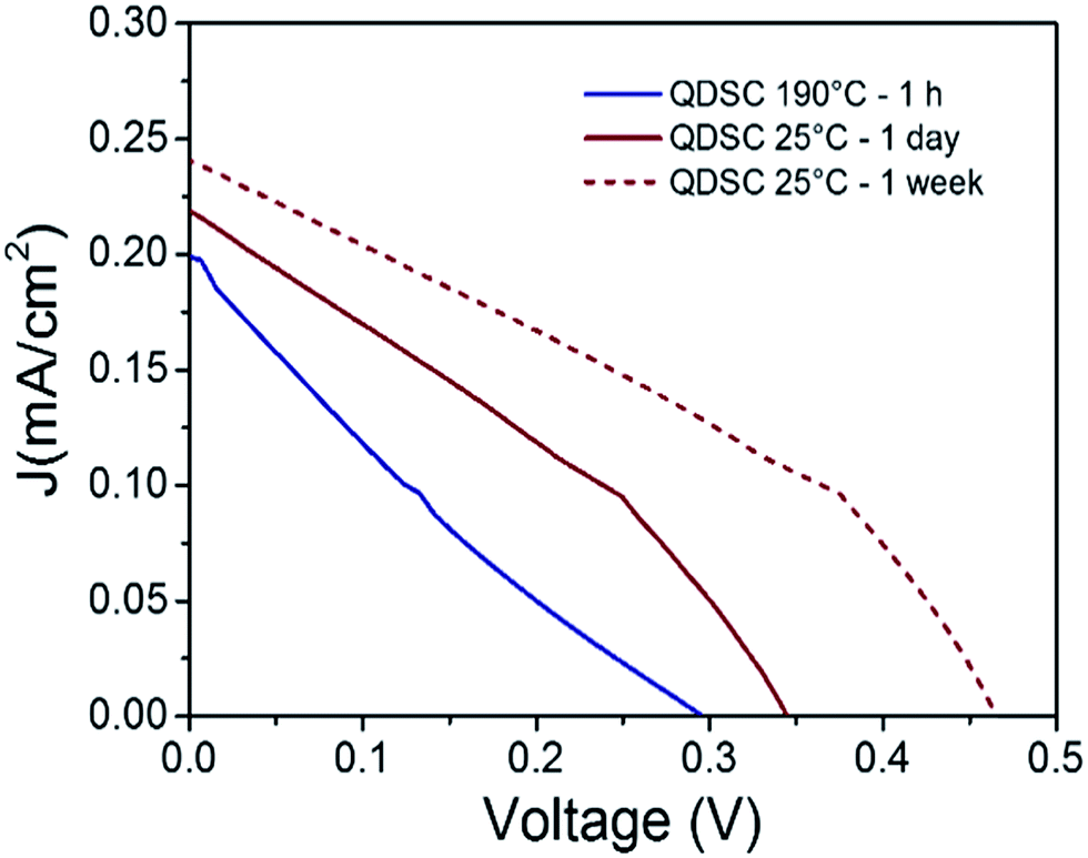 | ||
| Fig. 7 J/V curves of device annealed after HTM deposition, and devices left under N2 atmosphere at 25 °C (1 day to 1 week). Under AM1.5G 100 mW cm−2 illumination. | ||
| Jsc (mA cm−2) | Voc (V) | FF | PCE (%) | |
|---|---|---|---|---|
| QDSC (25 °C-1 day) | 0.22 ± 0.04 | 0.34 ± 0.0003 | 0.37 ± 0.001 | 0.028 ± 0.005 |
| QDSC (25 °C-1 week) | 0.25 ± 0.04 | 0.46 ± 0.0003 | 0.39 ± 0.001 | 0.045 ± 0.007 |
| QDSC (190 °C-1 h) | 0.20 ± 0.04 | 0.30 ± 0.0003 | 0.21 ± 0.001 | 0.013 ± 0.003 |
On the other hand, thermal annealing at 190 °C after Spiro-OMeTAD deposition (above the glass transition temperature, 125 °C (ref. 32)) led to lower PCE despite the expectation of pore filling increment.31 This performance reduction was ascribed to fast evaporation of the 4-tert-butylpyridine (tBP) additive during the heat treatment, starting at 85 °C. Usually, for solution deposition of the HTM layer, Spiro-OMeTAD is diluted in chlorobenzene with two additives: the lithium salt Li-TFSI and the tBP. Li-TFSI is expected to catalyze the Spiro-OMeTAD oxidation, and the tBP aids in LiTFSI dilution, keeping a homogeneous HTM layer after deposition. Although LiTFSI and tPB have been reported without any effect on the HTM conductivity, tBP adsorption into the active layer may influence the interfacial charge transfer improving both Voc and Jsc.33,34 Recently, remote molecular doping of QDs has been found35 to effectively p-dope QDs by compensation of trap states and contribution of free charge carriers through hole-injection into the QDs. In the present case, the tBP may act as oxidizing agent (p-dopant) due to its deeper HOMO level compared to the ionization energy of the CdSe QDs. Therefore, by using scanning Kelvin probe (SKP) the Fermi level of the CdSe active layer with and without tBP-treatment was measured, aiming to detect any shift induced by molecular doping. In fact, a shift of 0.062 eV toward a deeper energy level was measured after absorption of a tBP solution (0.015 mL mL−1 in acetonitrile) in the CdSe layer, indicating a weak p-doping.
Conclusions
This work explored a simple processing and direct assembly of WSQDs into hybrid photovoltaics. Ideal polarity of the capping agent is necessary to avoid either easy agglomeration or low QD concentration caused by high repulsion in solution. Narrow size distribution and surface coordination of the QDs determined the best power conversion performance. The growth period of the optimum QDs can be correlated to the brightpoint, where the best PLQY% and narrowest FWHM are reached simultaneously. Simultaneous increase of the Voc, Jsc and the PCE was achieved after thermal annealing of the CdSe QD layer and the room temperature infiltration of Spiro-OMeTAD. Annealing caused in situ growth of QDs and removed linked water and excess ligands, causing dense packing of the QDs and better electron-transport through the active layer. In addition, the improvement of Voc observed after further HTM infiltration can be ascribed to the surface passivation of in-gap trap states and weak p-doping of QDs induced by 4-tert-butylpyridine, as evidenced by Kelvin probe measurements. For future works, increasing the nanocrystal size to obtain larger hetero-interfacial contact area and higher light absorption can improve the photovoltaic performance, as long as proper energy alignment is kept. Larger CdSe QDs at their respective brightpoint can be obtained either by changing the synthesis conditions or increasing the growth temperature. Finding the brightpoint of larger QDs and surface passivation to obtain high quality WSQDs will be essential to compete with ORQDs. In addition, optimization of the HTM layer thickness is also required since infiltration can be limited by the reservoir of the HTM over-layer. Currently, we are advancing in impedance spectroscopy characterization to study the recombination and charge injection at the TiO2 NRs/CdSe QDs interface.Experimental
Materials and reagents
For synthesis of MSA capped CdSe QDs the following reagents were obtained: cadmium chloride 2.5 hydrate CdCl2·2,5H2O (Alfa Aesar, 80.7%), mercaptosuccinic acid (MSA) (Sigma-Aldrich, 97%), sodium borohydride NaBH4 (Panreac, 96%), sodium selenite Na2SeO3 (Sigma ∼98%) and sodium hydroxide NaOH (Sigma-Aldrich, 97%). For preparation of the solar cell prototypes the following materials were used: deionized water (DI, 18.2 MΩ cm), FTO glass slides (8 Ω sq−1 resistance) from Dyesol, Spiro-OMeTAD (2,2′,7,7′-tetrakis(N,N-di-p-methoxyphenylamine)-9,9-spirobifluorene). And titanium(IV) isopropoxide (TTIP, 97%), chlorobenzene (99,8%), 4-tert-butylpyridine (tBP, 96%), bis(trifluoromethylsulfonyl)amine lithium salt (LiTFSI, 99.95%) Aldrich, gold (Au, 99.99%), all from Sigma-Aldrich.Synthesis of MSA capped CdSe QDs
Briefly, the QDs were obtained by reaction of the respective precursors: Cd+2 and Se−2. Cadmium precursor was prepared by mixing 0.5659 g of CdCl2·2,5H2O and 0.4954 g of MSA in 100 mL of DI water. Later, the pH was adjusted to 11.0 by using a NaOH 0.1 M solution. Selenide precursor was obtained by reaction between 0.053 g of Na2SeO3 and 0.1 g of NaBH4 in 5 mL of water (colorimetric tube). After 6 minutes of reaction, Se−2 solution was added to the Cd+2 solution under magnetic stirring. These reactions were carried out inside a glovebox with N2 atmosphere.Growth of the CdSe NCs/obtaining NCs powder
The as-prepared QD solution (∼120 mL) was poured under room conditions into an autoclave of 200 mL, and once sealed it was introduced into an oven at 135 °C. When heating was over, 4/5 of the water was evaporated in vacuum (60–70 °C) to obtain a concentrated solution of ∼24 mL. This was followed by addition of 2-propanol (non-solvent) under stirring to precipitate the NCs. Then, the solution was subjected to centrifugation (1900 rpm) for 15 minutes. The supernatant was removed and the precipitate was re-diluted in deionized water to wash the NCs. Precipitation–dilution was repeated one more time and finally, the wet powder was dried inside a vacuum oven at 70 °C for 1 hour. Visible residual of water was drained before drying.Device fabrication
At first, the FTO substrates (2.0 × 2.5 cm2) were partially etched with zinc powder and HCl (2 M) to prevent short circuit (free area of 0.5 × 2 cm2), cleaned by hand with soap and deionized water, followed by sonication in a mixture 2-propanol/DI water/ethanol (1![[thin space (1/6-em)]](https://www.rsc.org/images/entities/char_2009.gif) :1:1 v/v) for 20 min. TiO2 NRs were prepared using hydrothermal method as reported elsewhere.23,24 Briefly, 1 mL of TTIP was added drop by drop into a mixture of DI water (25 mL) and HCl (25 mL–37 v/v), and kept under vigorous stirring to obtain a transparent solution. The solution was transferred to the Teflon liner of an autoclave where the FTO substrates were tilted against the inner wall, FTO face downward. The autoclave was placed inside a furnace and hydrothermal growth was conducted at 180 °C for 1.5 h to obtain TiO2 NR length of ∼600 nm. After the synthesis, the NR-substrates were taken out, rinsed with abundant DI water and dried in air. Additional surface treatment of the TiO2 NRs was carried out as follows. 1 mL of TTIP was added drop by drop into a mixture of DI water (39 mL) and HCl (830 μL–37 v/v), and kept under vigorous stirring for 1–1.5 h to obtain a transparent solution. Then, the solution was transferred to the Teflon liner of the autoclave where the substrates covered with TiO2 NRs were tilted against the inner wall, this time NRs face upward. The autoclave was placed into the furnace (pre-heated) and hydrothermal treatment was conducted at 90 °C for 1 h. When heating finished, the substrates were taken out, rinsed with DI water and dried in air. Later, the NRs were scratched off to uncover the FTO contact in one extreme of the substrates (0.5 × 2 cm2). Finally, the NR-substrates were annealed inside a furnace at 450 °C for 1 hour, and cooled down by natural convection (furnace off).
:1:1 v/v) for 20 min. TiO2 NRs were prepared using hydrothermal method as reported elsewhere.23,24 Briefly, 1 mL of TTIP was added drop by drop into a mixture of DI water (25 mL) and HCl (25 mL–37 v/v), and kept under vigorous stirring to obtain a transparent solution. The solution was transferred to the Teflon liner of an autoclave where the FTO substrates were tilted against the inner wall, FTO face downward. The autoclave was placed inside a furnace and hydrothermal growth was conducted at 180 °C for 1.5 h to obtain TiO2 NR length of ∼600 nm. After the synthesis, the NR-substrates were taken out, rinsed with abundant DI water and dried in air. Additional surface treatment of the TiO2 NRs was carried out as follows. 1 mL of TTIP was added drop by drop into a mixture of DI water (39 mL) and HCl (830 μL–37 v/v), and kept under vigorous stirring for 1–1.5 h to obtain a transparent solution. Then, the solution was transferred to the Teflon liner of the autoclave where the substrates covered with TiO2 NRs were tilted against the inner wall, this time NRs face upward. The autoclave was placed into the furnace (pre-heated) and hydrothermal treatment was conducted at 90 °C for 1 h. When heating finished, the substrates were taken out, rinsed with DI water and dried in air. Later, the NRs were scratched off to uncover the FTO contact in one extreme of the substrates (0.5 × 2 cm2). Finally, the NR-substrates were annealed inside a furnace at 450 °C for 1 hour, and cooled down by natural convection (furnace off).
Subsequently, for deposition of the CdSe QD layer, the NR-substrate was placed over a metal sheet (SS) and fastened to it with copper wire (dia. 0.25 mm) as shown in Fig. S4b (ESI†). The substrate was also blown off with compressed air to remove any speck of dust. Then, the assembly (substrate-sheet) was placed over a hot plate inside a fume hood, and the sheet was kept at 45–47 °C. Before deposition, the CdSe QD solution was always passed through a 0.22 μm syringe filter to remove large aggregates. Then, by using a micropipette, 0.27 mL of 10 mg mL−1 QD solution were dripped and distributed inside the limited area. Right after, the window of the fume hood was left with a small opening (8 cm) to let flow the room air at higher velocity. After 15 minutes the assembly was taken out, and the substrate removed from the sheet. Before HTM deposition, most devices were annealed at 190 °C for 1 h inside a vacuum oven (∼0.09 MPa). To deposit the HTM layer, a solution consisting of 72.3 mg Spiro-OMeTAD in 1 mL of chlorobenzene was prepared. Then, the solution was mixed with 28.8 μL of tBP and 17.5 μL of a stock solution: 520 mg lithium salt (LiTFSI) in 1 mL acetonitrile, and spin-coated onto the CdSe QD layers at 4000 rpm for 30 s under air conditions. Finally, the prototypes were completed by thermal evaporation of 57 nm thick gold counter-electrodes.
Characterization
UV-vis absorption spectra of QD solutions and CdSe QD layers (with TiO2 NRs film as blank) were obtained using a UV-vis-NIR scanning spectrophotometer Shimadzu UV-3101PC. Photoluminescence (PL) spectra were measured under excitation at 365 nm in a Jasco FP-8500 spectrometer. Average size and particle size distribution of the QDs were measured with high resolution transmission electron microscopy (HRTEM, JEOL JEM-2010). The cross section and layer thickness were examined with Field Emission Scanning Electron Microscopy (FESEM) using a Hitachi S-5500. The current–voltage (I–V) curves were recorded by a Keithley digital source meter and xenon arc lamp simulator (Oriel Sol 3A, Newport) with an AM1.5G spectral filter. The power density was calibrated to 1 sun illumination (100 mW cm−2). All the measurements were performed using a dark mask with an active area of ∼0.1 cm2. Measurements of the IPCE spectra were carried out using a Gamry PCI4-750 electrochemical system and a 100 W tungsten-halogen lamp (27 mW cm−2) coupled with a monochromator (Oriel 77250). The IPCE system was calibrated with a standard silicon photodiode. Infrared (IR) Spectroscopy by Attenuated Total Reflectance (ATR) was measured using a Perkin Elmer Spectrum GX. Film structure was characterized by X-ray diffraction (XRD) performed at a grazing angle of 5° with a Rigaku Diffractometer (D/MAX 2200) using the CuKα (λ = 1.54 Å) radiation source. Finally, the contact potential difference (CPD) measurements were conducted in a Kelvin probe station (KP Technology SKP-5050 system), using a 2 mm gold tip as reference (4.9 eV). Prior to the measurement, all the samples were allowed to stabilize in the dark.Acknowledgements
This work has been supported by DGAPA (UNAM-México) under Project No. IN103015, CONACYT-México under Projects No. 245754 and 270810, and the research groups: Laboratorio de óxidos metálicos y nanocarbono (IER-UNAM), FiQ-BioNanomat (Universidad del Valle – Colombia). M. A. T. would like to thank Colciencias-Colombia for his PhD fellowship. O. A. J.-Q. also would like to thank CONACYT for his PhD fellowship. Special thanks to Patricia Altuzar Coello, Gildardo Casarrubias Segura, Samuel Tehuacanero-Cuapa and Oscar Gómez Daza for their assistance in characterization techniques.References
- M. Liu, O. Voznyy, R. Sabatini, F. Pelayo, R. Munir, A. Balawi, X. Lan, F. Fan, G. Walters, A. Kirmani, S. Hoogland, F. Laquai, A. Amassian and E. Sargent, Nat. Mater., 2016, 4800, 1–7 Search PubMed.
- X. Lan, O. Voznyy, F. Pelayo García de Arquer, M. Liu, J. Xu, A. Proppe, G. Walters, F. Fan, H. Tan, M. Liu, Z. Yang, S. Hoogland and E. Sargent, Nano Lett., 2016, 16, 4630–4634 CrossRef CAS PubMed.
- N. Tomczak, D. Janczewski, M. Han and G. Vancso, Prog. Polym. Sci., 2009, 34, 393–430 CrossRef CAS.
- P. Reiss, E. Couderc, J. De Girolamo and A. Pron, Nanoscale, 2011, 3, 446–489 RSC.
- S. Bhattacharyya and A. Patra, J. Photochem. Photobiol., C, 2014, 20, 51–70 CrossRef CAS.
- A. Gaponik, D. Talapin, A. Rogach, K. Hoppe, E. Shevchenko, A. Kornowski, A. Eychmüller and H. Weller, J. Phys. Chem. B, 2002, 106, 7177–7185 CrossRef.
- W. Shibin, L. Chun and S. Gaoquan, Sol. Energy Mater. Sol. Cells, 2008, 92, 543–549 CrossRef.
- N. Kotov, I. Dekany and J. Fendler, J. Phys. Chem., 1995, 99, 13065 CrossRef CAS.
- R. Kniprath, J. Rabe, J. McLeskey, D. Wang and S. Kirstein, Thin Solid Films, 2009, 518, 295–298 CrossRef CAS.
- N. Gaponik, D. Talapin, A. Rogach and A. Eychmüller, J. Mater. Chem., 2000, 10, 2163–2216 RSC.
- M. Chen, H. Yu, S. Kershaw, H. Xu, S. Gupta, F. Hetsch, A. Rogach and N. Zhao, Adv. Funct. Mater., 2014, 24, 53–59 CrossRef CAS.
- X. Du, Z. Chen, F. Liu, Q. Zeng, G. Jin, F. Li, D. Yao and B. Yang, ACS Appl. Mater. Interfaces, 2016, 8, 900–907 CAS.
- S. Choi, H. Song, I. Park, J. Yum, S. Kim, S. Lee and Y. Sung, J. Photochem. Photobiol., A, 2006, 179, 135–141 CrossRef CAS.
- Y. Zhou, F. Riehle, Y. Yuan, H. F. Schleiermacher, M. Niggemann, G. Urban and M. Krüger, Appl. Phys. Lett., 2010, 96, 013304 CrossRef.
- K. Jeltsch, M. Schädel, J. B. Bonekamp, P. Niyamakom, F. Rauscher, H. Lademann, I. Dumsch, S. Allard, U. Scherf and K. Meerholz, Adv. Funct. Mater., 2012, 22, 397–404 CrossRef CAS.
- M. Eck, C. van Pham, S. Züfle, M. Neukom, M. Sessler, D. Scheunemann, E. Erdem, S. Weber, H. Borchert, B. Ruhstaller and M. Krüger, Phys. Chem. Chem. Phys., 2014, 16, 12251–12260 RSC.
- M. Eck and M. Krueger, Nanomaterials, 2016, 6, 1–12 CrossRef.
- M. M. Lee, J. Teuscher, T. Miyasaka, T. N. Murakami and H. J. Snaith, Science, 2012, 338, 643–647 CrossRef CAS PubMed.
- H. S. Kim, C. R. Lee, J. H. Im, K. B. Lee, T. Moehl, A. Marchioro, S. J. Moon, R. Humphry-Baker, J. H. Yum, J. E. Moser, M. Grätzel and N. G. Park, Sci. Rep., 2012, 2, 591 Search PubMed.
- Y. Wang, K. Yang, H. Pan, S. Liu and L. Zhou, Micro Nano Lett., 2012, 7, 889–891 Search PubMed.
- B. Dickerson, D. Irving, E. Herz, R. Claus, W. Spillman and K. Meissner, Appl. Phys. Lett., 2005, 86, 171915 CrossRef.
- W. Mi, J. Tian, W. Tian, J. Dai, X. Wang and X. Liu, Ceram. Int., 2012, 38, 5575–5583 CrossRef CAS.
- H. S. Kim, J. W. Lee, N. Yantara, P. Boix, S. Kulkarni, S. Mhaisalkar, M. Grätzel and N. G. Park, Nano Lett., 2013, 13, 2412–2417 CrossRef CAS PubMed.
- O. A. Jaramillo-Quintero, M. Solís de la Fuente, R. Sanchez, I. Recalde, E. Juarez-Perez, M. Rincón and I. Mora-Seró, Nanoscale, 2016, 8, 6271–6277 RSC.
- R. Meulenberg, J. Lee, A. Wolcott, J. Zhang, L. Terminello and T. Van Buuren, ACS Nano, 2009, 3, 325–329 CrossRef CAS PubMed.
- A. Kongkanand, K. Tvrdy, K. Takechi, M. Kuno and P. Kamat, J. Am. Chem. Soc., 2008, 130, 4007–4015 CrossRef CAS PubMed.
- V. Stevanovic, S. Lany, D. Ginley, W. Tumas and A. Zunger, Phys. Chem. Chem. Phys., 2014, 16, 3706–3714 RSC.
- A. Krishna, D. Sabba, H. Li, J. Yin, P. Boix, C. Soci, S. Mhaisalkar and A. Grimsdale, Chem. Sci., 2014, 5, 2702–2709 RSC.
- J. Jasieniak, M. Califano and S. Watkins, ACS Nano, 2011, 5, 5888–5902 CrossRef CAS PubMed.
- B. Hou, Y. Cho, B. Sung Kim, J. Hong, J. Bae Park, S. Jin Ahn, J. Inn Sohn, S. Cha and J. Min Kim, ACS Energy Lett., 2016, 1, 834–839 CrossRef CAS PubMed.
- C. Bailie, E. Unger, S. Zakeeruddin, M. Grätzel and M. McGehee, Phys. Chem. Chem. Phys., 2014, 16, 4864–4870 RSC.
- T. Leijtens, I. Ding, T. Giovenzana, J. Bloking, M. McGehee and A. Sellinger, ACS Nano, 2012, 6, 1455–1462 CrossRef CAS PubMed.
- Y. Fang, X. Wang, Q. Wang, J. Huang and T. Wu, Phys. Status Solidi A, 2014, 211, 2809–2816 CrossRef CAS.
- W. Nguyen, C. Bailie, E. Unger and M. McGehee, J. Am. Chem. Soc., 2014, 136, 10996–11001 CrossRef CAS PubMed.
- A. Kirmani, A. Kiani, M. Said, O. Voznyy, N. Wehbe, G. Walters, S. Barlow, E. Sargent, S. Marder and A. Amassian, ACS Energy Lett., 2016, 1, 922–930 CrossRef CAS.
Footnote |
| † Electronic supplementary information (ESI) available. See DOI: 10.1039/c7ra01055a |
| This journal is © The Royal Society of Chemistry 2017 |