 Open Access Article
Creative Commons Attribution 3.0 Unported Licence
Hydrogen incorporation effect in phosphorus-doped p-type ZnO thin films grown by radio-frequency magnetron sputtering
Min-Suk Oha and
R. Navamathavan *b
*b
aAutomotive Components and Materials R&D Group, Korea Institute of Industrial Technology (KITECH), Gwangju 61012, Korea
bDivision of Physics, School of Advanced Sciences, VIT University Chennai, Vandalur – Kelambakkam Road, Chennai – 600 127, India. E-mail: n_mathavan@yahoo.com; Fax: +91 44 3993 2555; Tel: +91 44 3993 1258
First published on 13th March 2017
Abstract
We report on the influence of hydrogen incorporation on the conductivity of phosphorous (P) doped ZnO thin films grown by using radio-frequency (RF) magnetron sputtering. The P dopant is an oxide form of P2O5, which is introduced into ZnO thin films using RF plasma with oxygen ambient to suppress the generation of O vacancies. The resultant P-doped ZnO thin films were analyzed by means of field-emission scanning electron microcopy (FE-SEM), atomic force microscopy (AFM), secondary ion mass spectroscopy (SIMS), Fourier transform infrared (FT-IR) spectroscopy, photoluminescence and Hall effect measurements. It was observed that the P2O5-doped ZnO thin films annealed at 800 °C exhibited the best electrical property with p-type behavior. Hydrogen atoms in ZnO thin films play an unusual role since it acts as a shallow donor and it may control the n-type conductivity in undoped material. Measurements revealed that the hydrogen atoms can be easily incorporated from the P-doped ZnO sputtering target as the natural hydrogen incorporation in P-doped ZnO thin films during magnetron sputtering. The role of hydrogen atoms incorporated in ZnO thin films is investigated by means of SIMS analysis.
Introduction
Wurtzite ZnO is a wide-bandgap semiconductor compound which offers fascinating optical and electrical properties, such as a direct wide band gap (∼3.4 eV), a low-power threshold (∼160 μJ cm−2) for optical pumping at room temperature and a large exciton binding energy (∼60 meV).1–4 It also has other advantages, such as the availability of larger area substrates, the amenability to wet chemical etching, a high radiation resistance and relatively low materials costs.5–9 Due to their attractive properties, ZnO thin films have been recognized as a promising candidate for applications in optoelectronic devices, such as light-emitting diodes, laser diodes and UV photodetectors.10,11 For the development of ZnO based optoelectronic devices, it is necessary to obtain p and n-type ZnO thin films. As a typical II–VI semiconductor, ZnO films are usually existed in n-type nature owing to the non-stoichiometry of the film, that is, the presence of oxygen vacancies or zinc interstitials. In order to realize ZnO based devices, fabrication of reliable p-type ZnO is essential. However, production of p-type ZnO is extremely difficult to achieve due to its self-compensating effect and low solubility of the acceptor dopant in ZnO.12,13 In this connection, so far many researchers have reported that p-type ZnO can be realized by the doping of arsenic, antimony, copper and nitrogen with hydrogen or group-III elements.14–18 It is also reported that p-type ZnO can be realized without doping by using well-optimized growth condition.19,20 Previously, we have demonstrated that the realization of phosphorus (P)-doped p-type ZnO thin films with a post thermal annealing activation process at 800 °C in an N2 ambient.21 These results indicated that the substitution of O atoms with large amount of P increases the residual strain in P-doped ZnO and consequently stacking faults form to release the strain.22 The main purpose of this work is to report the reason why post activation process is necessary and how the thermal energy affects phosphorus doped ZnO thin films by understanding the mechanism of acceptor activation in P-doped ZnO.In this work, we have investigated the effect of hydrogen incorporation on the conductivity of P-doped ZnO thin films grown by radio-frequency (RF) magnetron sputtering. The P dopant is an oxide form of P2O5, which is introduced into the ZnO thin film using RF plasma under an oxygen ambient to suppress the generation of O vacancies. The resultant P-doped ZnO thin films were analyzed by field-emission scanning electron microcopy (FE-SEM), atomic force microscopy (AFM), secondary ion mass spectroscopy (SIMS), Fourier transform infrared (FT-IR) spectroscopy, photoluminescence and Hall effect measurements. Our experimental observations indicated that the hydrogen atoms can be easily incorporated from the P-doped ZnO sputtering target as natural hydrogen atoms incorporation in P-doped ZnO thin films during magnetron sputtering. Hydrogen and phosphorous interact strongly to form a neutral defect complex, therefore as-grown P-doped ZnO thin films showed insulating electrical behavior.
Experimental procedure
The P-doped ZnO thin films were deposited on the semi-insulating undoped ZnO buffer layer which was grown on a c-plane Al2O3 substrate by using RF magnetron sputtering. The growth temperature was of 500 °C and the RF power was of 30 W. A commercially sintered 1 wt% phosphorus pentoxide (P2O5)-doped ZnO target with a 2 inch diameter was used for the sputtering process. Before starting the sputtering, the chamber was evacuated to a base pressure of ∼2 × 10⁻⁶ Torr. Then, the magnetron sputtering was performed in a mixed atmosphere of Ar and O2 gas with ratio of 3![[thin space (1/6-em)]](https://www.rsc.org/images/entities/char_2009.gif) :
:![[thin space (1/6-em)]](https://www.rsc.org/images/entities/char_2009.gif) 1. The working pressure was maintained at 10 mTorr. The thicknesses of the buffer layer and P2O5-doped ZnO were 0.7 and 0.8 μm, respectively. A rapid thermal annealing was conducted at the temperature in the range of 300 to 850 °C for 2 min in an N2 ambient in order to activate the acceptor (p-type carriers) in the ZnO thin films. Hall effect measurements were performed on the sample in the van der Pauw configuration (BIO-RAD HL5500 PC). An atomic force microscopy (AFM) was used to observe the surface morphology of the P2O5-doped ZnO samples. The surface morphology of the ZnO thin films was observed by using field-emission scanning electron microscopy (FE-SEM, Hitachi S-7400, Hitachi, Japan). In order to obtain the depth profiles of the hydrogen and phosphorous atoms in P2O5-doped ZnO thin films, a secondary ion mass spectrometry (SIMS, PHI 7200 TOF-SIMS/SALI) analysis was carried out by using a Cs+ ion beam. Fourier transform infrared spectroscopy (FTIR) was used to observe the –OH related bonding configuration in the P2O5-doped ZnO sputtering targets with P2O5 composition of 0.01–60 wt%. Photoluminescence (PL) spectra of P2O5-doped ZnO thin films were obtained by using a He–Cd laser (λ = 325 nm). Finally, the electrical properties of ZnO thin films were carried out by using a parameter analyzer (HP 4155A). Ti/Au (30 nm/50 nm) metal layers were deposited on the ZnO layers by electron-beam evaporation. The sample was annealed at 300 °C for 30 seconds in N2 ambient to enhance the contact behavior of Ti/Au electrode.
1. The working pressure was maintained at 10 mTorr. The thicknesses of the buffer layer and P2O5-doped ZnO were 0.7 and 0.8 μm, respectively. A rapid thermal annealing was conducted at the temperature in the range of 300 to 850 °C for 2 min in an N2 ambient in order to activate the acceptor (p-type carriers) in the ZnO thin films. Hall effect measurements were performed on the sample in the van der Pauw configuration (BIO-RAD HL5500 PC). An atomic force microscopy (AFM) was used to observe the surface morphology of the P2O5-doped ZnO samples. The surface morphology of the ZnO thin films was observed by using field-emission scanning electron microscopy (FE-SEM, Hitachi S-7400, Hitachi, Japan). In order to obtain the depth profiles of the hydrogen and phosphorous atoms in P2O5-doped ZnO thin films, a secondary ion mass spectrometry (SIMS, PHI 7200 TOF-SIMS/SALI) analysis was carried out by using a Cs+ ion beam. Fourier transform infrared spectroscopy (FTIR) was used to observe the –OH related bonding configuration in the P2O5-doped ZnO sputtering targets with P2O5 composition of 0.01–60 wt%. Photoluminescence (PL) spectra of P2O5-doped ZnO thin films were obtained by using a He–Cd laser (λ = 325 nm). Finally, the electrical properties of ZnO thin films were carried out by using a parameter analyzer (HP 4155A). Ti/Au (30 nm/50 nm) metal layers were deposited on the ZnO layers by electron-beam evaporation. The sample was annealed at 300 °C for 30 seconds in N2 ambient to enhance the contact behavior of Ti/Au electrode.
Results and discussion
The electrical properties of the P2O5-doped ZnO thin films annealed at different temperatures are summarized in Table 1. In order to check the reproducibility of the data, we have taken three samples which were annealed at different temperatures for 2 min in an N2 ambient. As-grown P2O5-doped ZnO thin film was observed to be of highly resistive nature, therefore, we could not measure the electrical properties of those samples. Similarly, P2O5-doped ZnO thin films annealed at relatively low temperature of the ranges of 300 and 500 °C were also observed to be of semi-insulating electrical behavior. However, the conductivity of P2O5-doped ZnO thin films started to show conversion of conductivity to p-type behavior beyond thermal annealing of 700 °C. With further increasing annealing temperature the phosphorus atom is dissociated from the P2O5 source and acting as an acceptor which is resulted in the formation of p-type ZnO thin films. It should be emphasized that all the samples annealed at 800 °C can be converted to p-type. We noticed a strange behavior for the samples annealed at 850 °C for which the conductivity behavior was observed to of n-type nature. In this study, the reason behind this phenomenon was investigated in detail and the results will be discussed in the following sections.| Temperature (°C) | Type | N (cm−3) | Mobility (cm2 V−1 s−1) | R (ohm per cm) | |
|---|---|---|---|---|---|
| As-grown | 1 | Insulator | — | ||
| 2 | — | ||||
| 3 | — | ||||
| 300 | 1 | Insulator | — | ||
| 2 | — | ||||
| 3 | — | ||||
| 500 | 1 | Insulator | — | ||
| 2 | — | ||||
| 3 | — | ||||
| 700 | 1 | Insulator | — | ||
| 2 | P | +2.36 × 10¹⁷ | 2.14 | 15.4 | |
| 3 | N | −7.67 × 10¹⁷ | 2.23 | 30.3 | |
| 800 | 1 | P | +4.14 × 10¹⁷ | 0.44 | 34.4 |
| 2 | P | +3.67 × 10¹⁷ | 0.49 | 35.7 | |
| 3 | P | +3.23 × 10¹⁷ | 0.5 | 38.2 | |
| 850 | 1 | N | −1.76 × 10¹⁷ | 23.7 | 0.15 |
| 2 | N | −1.93 × 10¹⁷ | 20.5 | 0.16 | |
| 3 | N | −1.54 × 10¹⁷ | 27.23 | 0.14 | |
Fig. 1(a)–(d) show the FE-SEM of ZnO thin films annealed at different temperatures. As can be seen from the FE-SEM images, the surface roughness was increased with increasing annealing temperature. The surface morphology of the ZnO thin films were further analyzed by means AFM. Fig. 2(a)–(d) show the AFM images of the P2O5-doped ZnO thin films before and after thermal annealing at different temperatures. It is observed that as-grown P2O5-doped ZnO thin film exhibited a smooth surface morphology as shown in Fig. 2(a). The root mean square (RMS) roughness of as-grown P2O5-doped ZnO thin film was of 2 nm, indicating an excellent structural property. Thus, it can be considered that 2-dimensional (2D) growth mode was established by optimization of magnetron sputtering condition. Comparing as-grown sample with the P2O5-doped ZnO thin films annealed at high temperatures of 700 to 850 °C exhibited much coarser surface morphology. The RMS roughness value of P2O5-doped ZnO thin film was of 4.53, 7.84, and 9.07 nm corresponding to the annealing temperature of 700, 800, and 850 °C, respectively. This result demonstrates that the surface roughness monotonically increases with increasing annealing temperature.
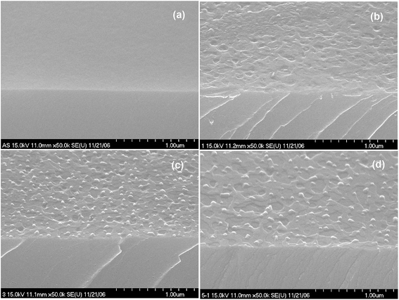 | ||
| Fig. 1 Surface morphology of P-doped ZnO annealed at different temperature for 2 min in an N2 ambient. (a) As-grown, (b) 700 °C, (c) 800 °C, and (d) 850 °C. | ||
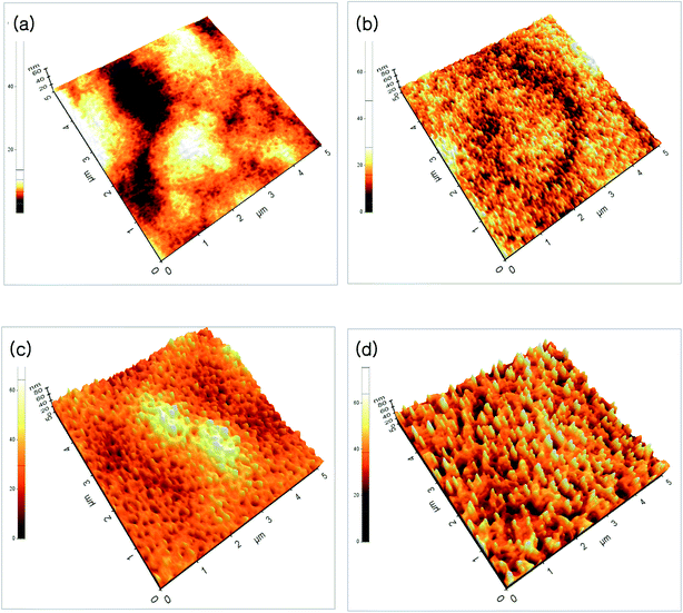 | ||
| Fig. 2 AFM images of P2O5-doped ZnO thin films before and after thermal annealing at different temperature. (a) As-grown, (b) 700 °C, (c) 800 °C, (d) 850 °C. | ||
To observe a correlation between impurity concentration and post thermal annealing temperature, we determined the distribution profile of hydrogen and phosphorous atoms in P2O5-doped ZnO thin films annealed at different temperatures by using SIMS analysis. Fig. 3(a) and (b) show the SIMS depth profiles for hydrogen and phosphorous atoms, respectively. The distribution profiles of each element were quantified by using hydrogen and phosphorous ion-implanted ZnO standards. The unintentionally doped high concentration of hydrogen atoms (∼2.5 × 10²⁰ atoms per cm3) was detected in the as-grown P2O5-doped ZnO thin films as shown in Fig. 2(a). It is expected that the hydrogen atoms can be easily incorporated in the ZnO thin films during the growth of chemical vapor deposition owing to the existence of hydrogen in Zn growth precursor itself.23,24 However, it is quite weird that ZnO thin films contained such a high hydrogen concentration is being grown in the physical vapor deposition chamber evacuated to a pressure of ∼10−6 Torr prior to the deposition. The presence of hydrogen atoms in ZnO is reported to be interstitial hydrogen (Hi) in the positive charge state of H+ to form Hi by making a strong bond with the anion (O2−) of ZnO to act as a shallow donor.25,26 It is noteworthy that all of the interstitial hydrogen atoms are not in a donor state because Hall effect measurement showed that as-grown P2O5-doped ZnO thin film was observed to be highly resistive insulator. This result indicates that most of the compensating or compensated hydrogen atoms are in an inactive state in as-grown P2O5-doped ZnO thin films. This high concentration of hydrogen atoms proportionally decreased as the annealing temperature increased. At an annealing temperature above 800 °C, H concentration was significantly reduced in P2O5-doped ZnO thin films. It is also seen that area up to 0.4 μm below the surface was more sensitively affected by thermal annealing treatment, showing abrupt change of hydrogen atom concentration. It should be emphasized that undoped ZnO buffer layer did not contain hydrogen atoms even though it was grown under the same coating condition with P2O5-doped ZnO thin films. Fig. 3(b) shows the distribution of P dopant atoms in P2O5-doped ZnO thin films. It shows that the concentration of P atoms (∼3.3 × 10²⁰ atoms per cm3) remain almost constant even though annealing temperature was higher than 800 °C. Only a small amount of P atoms diffused into the underlying undoped buffer ZnO layer during thermal annealing process.
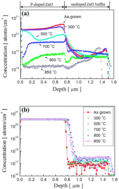 | ||
| Fig. 3 SIMS depth profiles of (a) hydrogen atoms and (b) phosphorus atoms in P2O5-doped ZnO thin films before and after thermal annealing. | ||
In order to investigate the oxygen concentration variation, the O concentration was measured by using SIMS analysis as shown in Fig. 4. As can be seen from the data, the reduction of O concentration is observed with the increasing annealing temperature. However, an abrupt change of O concentration in the surface area was not observed. We believe that further study is required to understand the process clearly. Currently, we are planning for the systematic measurements to investigate the effect of thermal annealing on surface variation of P-doped ZnO thin films.
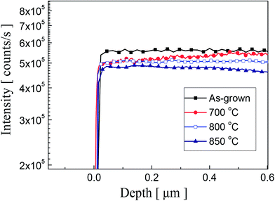 | ||
| Fig. 4 SIMS depth profiles of oxygen atoms in P2O5-doped ZnO thin films before and after thermal annealing. | ||
To investigate the origin of unintentionally high concentration of H atoms which act as an acceptor compensating defect in P2O5-doped ZnO thin films, the FTIR absorption spectra of powdered P2O5-doped ZnO sputtering target was observed as shown in Fig. 5. The P2O5 doping composition in the sputtering target was adjusted from 0.01 to 60 wt%. For comparison, undoped ZnO and 2 wt% Al-doped ZnO target was also investigated in the present study. The absorption peak around 3400 cm−1 is attributed to the local stretch mode of H bonded to O atoms.23,27 As shown in Fig. 5, the intensity of the O–H absorption peak linearly increased with an increase of P2O5 doping concentration. It should be noted that O–H absorption peak was not detected in the undoped ZnO target and 2 wt% Al-doped ZnO target, indicating that the incorporation of H is strongly related to the presence of P2O5 in the ZnO target.
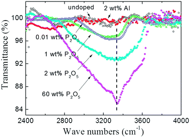 | ||
| Fig. 5 FT-IR transmittance spectra of P2O5-doped ZnO sputtering targets. For comparison, undoped ZnO and 2 wt% Al-doped ZnO target was also investigated. | ||
The chemical compound P2O5 is conventionally prepared by burning elemental phosphorus with sufficient supply of air as expressed by a following chemical reaction equation.28
| P4 + 5O2 → P4O10 |
However, it is a potent dehydrating agent as indicated by the exothermic nature of its hydrolysis.
| P4O10 + 6H2O → 4H3PO4 (−177 kJ mol−1) |
Therefore, it can be thought that unexpectedly high concentration of H in P2O5-doped ZnO thin films grown in the high vacuum system originated from P2O5-doped ZnO target which absorbing ambient water molecules (H2O) to form H3PO4. It should be noted that 0.01 wt% and 1 wt% P2O5-doped ZnO targets showed nearly identical peak intensity, indicating a very small amount of P2O5 absorbed a quite large amount of H2O, as shown in Fig. 5.
Fig. 6 shows the average hydrogen atom concentration in the P2O5-doped ZnO thin films as a function of post thermal annealing temperatures and the activation energies (EA) estimated from Arrhenius plots of hydrogen atom concentration versus reciprocal thermal annealing temperature. The activation energies of hydrogen atoms in the region I (below 500 °C) and II (above 700 °C) were calculated to be 2.8 ± 0.1 eV and 4.91 ± 0.42 eV, respectively. The activation energy in region I corresponds to the bond strength of H–P bond (2.97 eV). The activation energy of the H atoms in region II was estimated to be 4.91 ± 0.42 eV. This value is close to the H–O bond strength of 4.33 eV. These results indicate that acceptor compensating hydrogen atoms in P2O5-doped ZnO thin film make a strong bond to P and/or O atoms. And also it is indicative of the dissociation of H–P and/or H–O complexes and the out diffusion of H from the film during post thermal annealing at the temperature above 700 °C. It is also expected that this high annealing temperature contemporarily induced the substation of O with P, increasing hole concentration in P2O5-doped ZnO thin films by making stacking faults in the P2O5-doped ZnO lattice.22
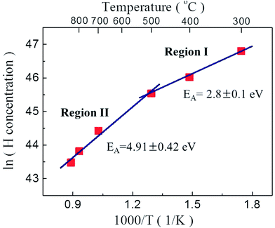 | ||
| Fig. 6 Activation energies (EA) from Arrhenius plots of hydrogen concentration versus reciprocal thermal annealing temperature. | ||
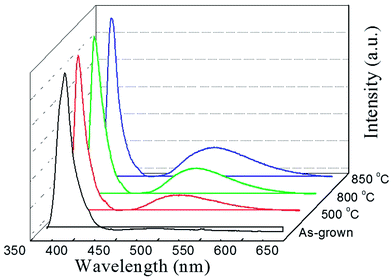
To investigate the abnormal n-type conductivity in P2O5-doped ZnO films after removing compensating hydrogen atoms at an annealing temperature of 850 °C, the room temperature PL spectra of the P2O5-doped ZnO thin films annealed at different temperature in the range of 500–850 °C were obtained as shown in Fig. 7. For comparison, the PL data of as-grown P2O5-doped ZnO sample was also measured. All the ZnO samples exhibited a near-bandedge emission at about 387 nm. It was found that post thermal annealing did not affect the intensity of the narrow near-bandedge emission peaks. However, the intensity of the broad green emission peaks was monotonically increased when the P2O5-doped ZnO samples were thermally annealed. The intensities of the green emission peak were increased proportionally with increasing annealing temperature. It is well known that such a broad deep level emission is closely related to intrinsic defects, such as Zn interstitial (Zni), oxygen vacancies (VO) and Zn anti-site (OZn), which are generally thought to act as donor defects.29,30 These results suggest that a high temperature annealing of P2O5-doped ZnO thin films caused the dissociation of the Zn–O bonds near the surface region and inducing the preferential evaporation of oxygen atoms. The formation of VO results in an increase of electron concentration of the films. The roughened surface of annealed P2O5-doped ZnO as shown in Fig. 1 was probably due to this preferential evaporation of O from the surface. Abundant donor defects near the surface region induced by post thermal annealing at 850 °C probably provided the current path during Hall measurement, resulting in n-type conductivity of P2O5-doped ZnO. These results imply that post thermal annealing of P2O5-doped ZnO thin films at high temperature could facilitate the mixed conductivity like the inhomogeneous doping of N or As acceptor-doped ZnO thin films grown by metal–organic chemical vapor deposition.31 Therefore, it can be concluded that post thermal annealing conditions for acceptor activation, such as annealing temperature and holding time, should be precisely optimized in order to realize the reproducible and reliable p-type ZnO thin films using P2O5 dopants.
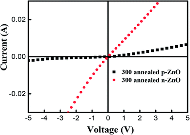
To further confirm the existence of p-type conductivity of P-doped ZnO thin films, we have performed the current–voltage (I–V) measurements by using a parameter analyzer. Fig. 8 shows the I–V characteristics of Ti/Au metal contacts on P-doped ZnO thin films. It is observed that the Ti/Au contacts to the sample annealed at 850 °C shows linear I–V characteristic indicating that the formation of a good ohmic contact. On the other hand, the contact to the sample annealed at 800 °C exhibited a leaky Schottky behavior. The I–V characterization result implies that the electrical conductivity of P-doped ZnO layer annealed at 850 °C and layer annealed at 800 °C are n-type and p-type ZnO, respectively.
Conclusions
We have demonstrated that the role of hydrogen incorporation on the conductivity of P doped ZnO thin films grown by using radio-frequency (RF) magnetron sputtering. The resultant ZnO thin films were characterized for their morphological, structural, optical and electrical properties. The RMS roughness value of P2O5-doped ZnO thin films were increased with increasing annealing temperature. At elevated annealing temperature the phosphorus atoms were easily dissociated from the P2O5 source and plays the role as an acceptor which resulted in the formation of p-type ZnO thin films. It was observed that the P2O5-doped ZnO thin films annealed at 800 °C exhibited the best electrical property with an acceptor concentration of 3.23 × 1017 cm−3, mobility of 0.5 cm2 V−1 s−1 and resistivity of 35.7 ohm per cm. The activation energies calculations revealed that the acceptor compensating H atoms in P2O5-doped ZnO thin films make a strong bond to P and/or O atoms. Hydrogen atoms in ZnO thin films play an unusual role since it acts as a shallow donor and it may control the n-type conductivity in undoped material.Notes and references
- D. K. Hwang, M. S. Oh, J. H. Lim and S. J. Park, J. Phys. D: Appl. Phys., 2007, 40, R387 CrossRef CAS.
- J. O. Song, K. K. Kim, S. J. Park and Y. Y. Seong, Appl. Phys. Lett., 2003, 83, 479 CrossRef CAS.
- C. Zhang, F. Zhang, T. Xia, N. Kumar, J. Hahn, J. Liu, Z. L. Wang and J. Xu, Opt. Express, 2009, 17, 7893 CrossRef CAS PubMed.
- S. I. Park, Y. Tchoe, H. Baek, J. Heo, J. K. Hyun, J. Jo, M. Kim, N. J. Kim and G. C. Yi, APL Mater., 2015, 3, 016103 CrossRef.
- A. Tsukazaki, A. Ohtomo, T. Onuma, M. Ohtani, T. Mahino, M. Sumiya, K. Ohtani, S. F. Chichibu, S. Fuke, Y. Segawa, H. Ohno, H. Koinuma and M. Kawasaki, Nat. Mater., 2005, 4, 42 CrossRef CAS.
- J. H. Lim, C. K. Kang, K. K. Kim, I. K. Park, D. K. Hwang and S. J. Park, Adv. Mater., 2006, 18, 2720 CrossRef CAS.
- Y. Y. Xi, Y. F. Hsu, A. B. Djurisic, A. M. C. Ng, W. K. Chan, H. L. Tam and K. W. Cheah, Appl. Phys. Lett., 2008, 92, 113505 CrossRef.
- K. S. Kim, F. Lugo, S. J. Pearton, D. P. Norton, Y. L. Wang and F. Ren, Appl. Phys. Lett., 2008, 92, 112108 CrossRef.
- Z. Y. Xiao, Y. C. Liu, R. Mu, D. X. Zhao and Y. J. Zhang, Appl. Phys. Lett., 2008, 92, 052106 CrossRef.
- Y. R. Ryu, S. Zhu, D. C. Look, J. M. Wrobel, H. M. Jeong and H. W. White, J. Cryst. Growth, 2000, 216, 330 CrossRef CAS.
- S. Tuzemen, G. Xiong, J. Wilkinson, B. Mischuck, K. B. Ucer and R. T. Williams, Phys. B, 2001, 308, 1197 CrossRef.
- C. H. Park, S. B. Zhang and S. H. Wei, Phys. Rev. B: Condens. Matter Mater. Phys., 2002, 66, 073202 CrossRef.
- S. J. Pearton, D. P. Norton, K. Ip, Y. W. Heo and T. Steiner, J. Vac. Sci. Technol., B: Microelectron. Nanometer Struct.--Process., Meas., Phenom., 2004, 22, 932 CrossRef CAS.
- Y. R. Ryu, T. S. Lee and H. W. White, Appl. Phys. Lett., 2003, 83, 87 CrossRef CAS.
- S. Limpijumnong, S. B. Zhang, S. H. Wei and C. H. Park, Phys. Rev. Lett., 2004, 92, 155504 CrossRef PubMed.
- D. B. Buchholz, R. P. H Chang, J. Y. Song and J. B. Ketterson, Appl. Phys. Lett., 2005, 87, 082504 CrossRef.
- K. Minegishi, Y. Koiwai, Y. Kikuchi, K. Yano, M. Kasuga and A. Shimizu, Jpn. J. Appl. Phys., 1997, 36, L1453 CrossRef CAS.
- M. Joseph, H. Tabata, H. Saeki, K. Ueda and T. Kawai, Phys. B, 2001, 302–303, 140 CrossRef.
- M. S. Oh, S. H. Kim and T. Y. Seong, Appl. Phys. Lett., 2005, 87, 122103 CrossRef.
- G. Xiong, J. Wilkinson, B. Mischuck, S. Tüzemen, K. B. Ucer and R. T. Williams, Appl. Phys. Lett., 2002, 80, 1195 CrossRef CAS.
- D. K. Hwang, M. S. Oh, J. H. Lim, C. G. Kang and S. J. Park, Appl. Phys. Lett., 2007, 90, 021106 CrossRef.
- M. S. Oh, D. K. Hwang, Y. S. Choi, J. W. Kang, S. J. Park, C. S. Hwang and K. I. Cho, Appl. Phys. Lett., 2008, 93, 111905 CrossRef.
- X. Li, B. Keyes, S. Asher, S. B. Zhang, S. H. Wei, T. J. Coutts, S. Limpijumnong and C. G. Van de Walle, Appl. Phys. Lett., 2005, 86, 122107 CrossRef.
- J. Dai, H. Su, L. Wang, Y. Pu, W. Fang and F. Jiang, J. Cryst. Growth, 2006, 290, 426 CrossRef CAS.
- M. G. Wardle, J. P. Gross and P. R. Briddon, Phys. Rev. Lett., 2006, 96, 205504 CrossRef CAS PubMed.
- M. S. Oh, D. K. Hwang, J. H. Lim, Y. S. Choi and S. J. Park, Appl. Phys. Lett., 2007, 91, 212102 CrossRef.
- S. C. Lim, S. H. Kim, J. B. Koo, J. H. Lee, C. H. Ku, Y. S. Yang and T. Zyung, Appl. Phys. Lett., 2007, 90, 173512 CrossRef.
- R. E. Threlfall, The story of 100 years of Phosphorus Making: 1851 – 1951, Albright & Wilson Ltd, Oldbury, 1951 Search PubMed.
- M. Liu, A. H. Kitai and P. Mascher, J. Lumin., 1992, 54, 35 CrossRef CAS.
- G. W. Tomlis, J. L. Routbort and T. O. Mason, J. Appl. Phys., 2000, 87, 117 CrossRef.
- A. Krtschil, A. Dadgar, N. Oleynik, J. Blasing, A. Diez and A. Krost, Appl. Phys. Lett., 2005, 87, 262105 CrossRef.
| This journal is © The Royal Society of Chemistry 2017 |

