 Open Access Article
Creative Commons Attribution 3.0 Unported Licence
Controlling the conductivity of Ti3C2 MXenes by inductively coupled oxygen and hydrogen plasma treatment and humidity
Florian M. Römer *a,
Ulf Wiedwalda,
Tanja Struscha,
Joseph Halimb,
Elisa Mayerbergerb,
Michel W. Barsoumb and
Michael Farle
 a
a
aFaculty of Physics and Center for Nanointegration (CENIDE), University of Duisburg-Essen, Lotharstr. 1, 47057 Duisburg, Germany. E-mail: florian.roemer@uni-due.de; Tel: +49 203 379 4411
bDepartment of Materials Engineering, LeBow Engineering Center 27-445, Drexel University, Philadelphia, PA 19104-2875, USA
First published on 24th February 2017
Abstract
We report on the effects of plasma treatment and humidity on the electrical conductivities of Ti3C2 MXene thin films. The latter – spincoated from a colloidal solution produced by LiF/HCl etching of Ti3AlC2 powders – were 13 nm thick with an area of 6.8 mm2. The changes in the films exposed to hydrogen (H) and oxygen (O) plasmas in vacuum were analyzed by X-ray photoelectron spectroscopy. We find that the film resistivities can be switched reproducibly by plasma treatment between 5.6 μΩm (oxidized state) to 4.6 μΩm (reduced state). Both states show metallic like conductivity. In high vacuum, the film resistivity was 243 Ω; when the relative humidity was 80% the film resistance increased to 6340 Ω, a 26 fold increase.
1 Introduction
Two dimensional (2D) materials have garnered huge interest in the scientific community due to their extraordinary electronic, chemical, optical, mechanical and structural properties.1 This interest started with the isolation of a single layer of carbon (graphene) and the determination of its electronic characteristics.2 Since then 2D materials have been of interest as sensing materials for various types of sensors.3,4 For instance, graphene demonstrated a potential as a sensing material for electrochemical sensors,5 hydrogen peroxide,6 glucose,7 nucleic acids,7 and protein markers detectors8 for biological sensors. In addition gases such as nitrogen oxide, NO2,9 hydrogen sulphide H2S,10 H2 11 and ammonia, NH3,12 can be detected. Similarly, other 2D materials such as transition metal dichalcogenides have demonstrated potential as materials for gas sensing and optoelectronic devices.13,14 For example, Li et al. fabricated transistors made from single- and few-layers MoS2 sheets that act as sensitive detectors for nitrous oxide NO gas.15 He et al. fabricated a flexible MoS2 thin film that demonstrated sensitivity of detection also for NO2 gas.16 Furthermore, the resistances of thin VS2 films were shown to demonstrate sensitivity to moisture.17 The main principle of 2D sensor devices is based upon changes in their conductance due to the adsorption of chemical or biological species which can act as electron donors or acceptors.18Recently a new family of 2D transition metal carbides labelled MXene was discovered.19 MXenes are produced by the selective etching of the A layers from the MAX phases.20 The latter, in turn, are a large family of layered ternary transition metal carbides, with a chemical formula Mn+1AXn where M is an early transition metal, A is an A-group element (mostly groups 13 and 14) of the periodic table of elements, X is C or/and N and n = 1 to 3. Because during etching the A-group element, typically Al, is replaced by –O, –OH and –F terminations,21,22,23 the proper designation of the resulting 2D material is Mn+1CnTx, where T represents a surface termination. MXenes have been fabricated in the form of multilayers19 and films.24 Thin films of Ti3C2Tx were fabricated via various methods such as magnetron sputtering of the MAX phase on a sapphire substrate followed by etching of Al using HF or NH4HF2,24,26 or through directly coating substrates with a colloidal solution of MXene by spray coating,25 spin coating26 or electrohydrodynamic atomization.27 The most studied MXene to date is Ti3C2Tx which has already shown potential for use in a number of diverse applications, such as batteries,28,29,30 supercapacitors,31,32 fuel cells,33 transparent conducting electrodes,24 photocatalytic applications,34 and water treatment.35 Most of the studies investigated thin films, but single flakes were also characterized by Miranda et al.36.
Furthermore, MXenes demonstrated potential as sensors. Nanocomposites of TiO2–Ti3C2Tx displayed good performance and excellent long term stability for sensing H2O2, making it promising for biosensors applications.37,38 Multilayered Ti3C2Tx was used to immobilize hemoglobin to fabricate a mediator-free biosensor showing good protein bioactivity and stability.18,37 Xu et al. demonstrated the capability of using a few layers of Ti3C2Tx in a field effect transistor (FET) for probing neural activity and detecting neural transmitters.39 Moreover, several theoretical studies showed the potential of MXenes to be used as gas sensing materials.40,41
Of special interest herein is the work of Dillon et al.26 who characterized spin coated Ti3C2Tx films. They showed that the conductivities of these films are a function of atmosphere; when stored in dry N2 the sheet conductance was greater than when the films were stored in the open atmosphere or humid N2. They also showed that the figures of merits of these transparent conductive films rivalled those of chemical vapor deposited undoped graphene films.
The purpose of this work is twofold. The first is to shed some more light on the effect of humidity on transport properties and its possible application as nanosize sensors. The second is to explore methods to further enhance their conductivities in general. To that effect we measured the conductivities of spin coated films after exposure to oxygen and hydrogen plasmas. We also measured the transport properties as a function of humidity and compared the response to a commercial humidity sensor.
2 Experimental details
2.1 Sample preparation
![[thin space (1/6-em)]](https://www.rsc.org/images/entities/char_2009.gif) :
:![[thin space (1/6-em)]](https://www.rsc.org/images/entities/char_2009.gif) 10 ml etching solution for 24 h at 35 °C. The powders were washed via a centrifugation and decantation process with three washes each of 6 mol/1 HCl§, 1 mol/1 LiCl, and distilled water in the ratio of 40 ml of solvent to 0.5 g of MAX powder. Approximately 10 ml of distilled water was added to the reaction mixture after the final decantation, shaken using a mechanical agitator to disperse the sediment throughout the solution, and sonicated for 1 h at room temperature under argon (Ar) gas. The mixture was centrifuged at 5000 rpm for 1 h followed by sonication, and the supernatant was collected.
10 ml etching solution for 24 h at 35 °C. The powders were washed via a centrifugation and decantation process with three washes each of 6 mol/1 HCl§, 1 mol/1 LiCl, and distilled water in the ratio of 40 ml of solvent to 0.5 g of MAX powder. Approximately 10 ml of distilled water was added to the reaction mixture after the final decantation, shaken using a mechanical agitator to disperse the sediment throughout the solution, and sonicated for 1 h at room temperature under argon (Ar) gas. The mixture was centrifuged at 5000 rpm for 1 h followed by sonication, and the supernatant was collected.This procedure results in an optimized delamination and cleanliness: a mixture of HCl and LiF is used to convert MAX phase Ti3AlC2 to Ti3C2Tx where the Al layers are selectively etched and replaced by a mixture of surface terminations:23 O, OH and/or F in addition to the intercalation of Li ions. However LiF can not be washed sufficiently using just water, so several washes with HCl were required to remove all the LiF residual salts but this also removes the Li ions between the layers. The latter is necessary for delamination. In order to intercalate Li ions back to the MXene, washing MXene in LiCl is required. LiCl is soluble in water and can be easily washed with it while preserving the Li ions intercalated in MXene.42
2.2 Measurements techniques
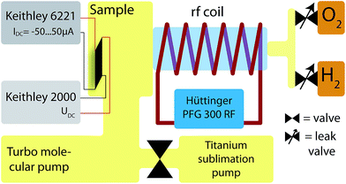
Schematics of the experimental setup are shown in Fig. 1 and 2. A vacuum chamber43,44 with a base pressure of 5 × 10⁻⁷ Pa (5 × 10⁻⁹ mbar)¶ is pumped by a turbo pump|| and a Titan sublimation pump. The latter is separated by a valve during plasma treatment and firing of the Titanium pump, to prevent Ti covering the sample.To couple the electromagnetic waves to the gas in the vacuum chamber a metal glass adapter is surrounded by 6 windings of 5 mm copper tubes. A modified radio frequency (rf) generator** at 13.56 MHz is used to excite plasma in the glass tube and chamber. Hydrogen (H) and oxygen (O) are connected to the chamber via two separate leak valves. At a pressure (p) of pH = 15 Pa (0.15 mbar) for H and pO = 5 Pa (5 × 10⁻² mbar) for O of ≥99.998% purity, an rf power of 20 W was applied through the coil. When using the O plasma, the pressure was doubled for 1–3 seconds to get a more homogeneous plasma, especially at the samples position. At a distance of 30 mm from the sample a thermocouple was positioned to detect the temperature rise due to the plasma treatment. At 20 W and 40 W rf power (P) the temperature increases by 6 K and 10 K, respectively. 80% of the overall temperature change is reached after 10 min. It was shown, that using this setup nano structures can be reduced very well.45
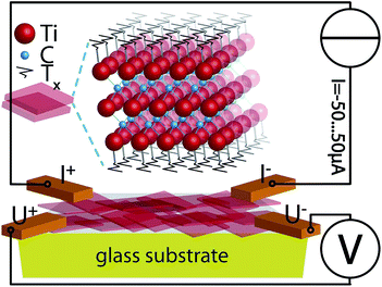
The sample was 4-point-contacted at the corners of a rectangular film (see Fig. 1). Current (I)–voltage (V) curves were measured using a constant current (Keithley™ 6221) I = −50…50 μA and a multimeter††. For more details see captions of Fig. 3 and 5.
XPS spectra were measured using non-monochromatic Al Kα radiation and a hemispherical electron energy analyzer.‡‡ Details are described in ref. 46. Here, is it better to say, that we used an in situ plasma treatment to judge the chemical changes and mimick the transport measurements. Ar sputtering is often used for cleaning, but our low energy plasma is more gentle, i.e. chemical etching instead of sputtering.
Humidity was measured by a commercial sensor§§ with a nominal detection range of 20–80r.h.% and and error bar of 5%r.h..
3 Results
In Section 3.1 we describe the results of the plasma induced resistivity changes and in 3.2 we discuss results of the observed humidity induced changes. Both findings show the potential of using MXenes as materials for transparent gas and humidity sensors.3.1 Plasma treated samples
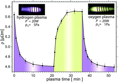
Further H plasma treatment reduces the resistivity with an exponential decay down to 4.62 μΩ m. The resistivity decreases by 18% to 82% of the start value of 5.64 μΩ m within 11 min. We assume that in this step the known OH termination23 reacts with H from the plasma to form steam, which is pumped away. H atoms may remain bonded at the MXene surfaces, however.
At t = 21 min in Fig. 3, the O plasma is switched on. Within one minute, the resistivity increases to 4.89 μΩ m. Further O plasma treatment increases the resistivity logarithmically as a function of time to 5.71 μΩ m which is similar to the initial value (only 1% above). Another series of H plasma treatments reduces the resistivity reproducibly to the previous H treated value to within <0.5%. Thus the resistivity of this MXene can be reversibly changed by 18%, presumably due to the removal of O that decreases the resistivity.
It is worth noting that when the same sample was treated with a power of 30 W an irreversible change, to higher resistivities values was observed presumably due to an irreversible oxidation of the MXene sheets.
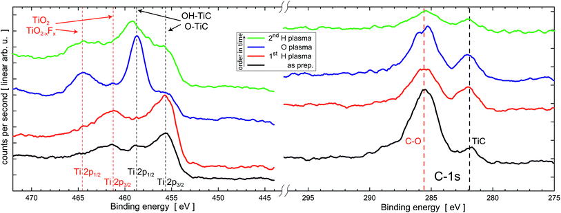 | ||
| Fig. 4 XPS spectra of MXene after several plasma etching steps. Ti (2p peaks) and C (1s peak) indicate a gradual oxidation and removal of O after subsequent O and H plasma treatments at 20 W plasma power for 20 min, respectively. Vertical lines indicate reference values for various compounds from the literature47 and ref. 23. After evaluation of the peak positions and intensities right (low binding energy) and left side (high binding energy) are individually scaled, shifted on the ordinate and smoothed using the Savitzky–Golay algorithm for better visualization. Quantitative analysis can be found in Table 1. | ||
In the as prepared state, the XPS spectra of the Ti-2p region show peaks belonging to MXene (O, OH–Ti–C) and titanium oxide and oxyfluoride (TiO2/TiO2−xFx),23 while the C-1s has a prominent peak at about 286 eV belonging to C–O contamination and a smaller peak at 282 eV belonging to the carbide component in MXene as shown in Fig. 4. After the first H plasma treatment for surface cleaning and possible removal of O of the Ti3C2 films, we observe a reduction of the C–O component and a slightly increased intensity of the MXene peak at 282 eV. At 686 eV (not shown here) a small peak attributed to F is observed. This overall finding is ascribed to the removal of typical carbon containing surface contaminants after transfer in ambient conditions.
The peaks belonging to MXene are increased compared to those belonging to oxides and oxyflorides. Thus, H plasma etching does not change the chemical state of the Ti3C2 MXene significantly.
After O plasma etching the spectral weight of the TiO2 and/or TiO2−xFx component rises strongly while the residual TiC component decreases but remains clearly visible. The C-1s peaks remain more or less unchanged. The F peak vanishes in the noise. Subsequent H plasma does not completely reduce the specimen to its initial state, however, the spectral weight changes towards the Ti–C bonds providing possible evidence for a partial reversible removal of O.
The spectral weight of the different components (Ti–C and Ti–O2) in the Ti-2p spectra are analyzed in more detail after subtracting the Shirley background for all sample states in Fig. 4. Within the error bar, and given quality of the data, the oxyfluoride content is not significant. It is therefore combined with TiO2. Table 1 presents the results of this fitting. The error bar has been evaluated during fitting assuming certain spectral weights and direct comparison to the experiments.
| State | TiC | TiO2 |
|---|---|---|
| As prep | 69 ± 4% | 31 ± 4% |
| After 1st H plasma | 71 ± 4% | 29 ± 4% |
| After 1st O plasma | 33 ± 4% | 67 ± 4% |
| After 2nd H plasma | 46 ± 4% | 54 ± 4% |
As discussed above the relative weight of 69 ± 4% of TiC and 31 ± 4% TiO2 components remains unchanged after H plasma treatment within the error bar. O plasma, however, oxidizes the Ti in the specimen significantly. The spectral weight of the oxide peaks increases to 67 ± 4%. Presumably the top and bottom layers of the Ti3C2 sheets are oxidized, thus changing the surface termination of MXenes. In turn, this observation explains the change in resistivity in Fig. 3. The underlying I–V curves suggest that subsequent H plasma treatment reduces the specimen to the initial state allowing for switching between high and low resistance states. XPS clearly shows this tendency. The initial state, however, is not reached after 20 min H plasma, and the result is a TiO2 content of 54 ± 4%. These results are important because they suggest that it is possible to affect the transport properties of MXene films by changing their terminations. We note that at 3 × 1022 cm−3 the carrier densities in Ti3C2Tx are quite high indeed and thus cannot be readily affected by changing the nature of the terminations.26 The most likely mechanisms for the variations are probably due to: (1) changing the resistance of the interlayer contacts (see below) and/or, (2) the electron mobilities are affected by plasma treatments.
3.2 Humidity dependent resistivity
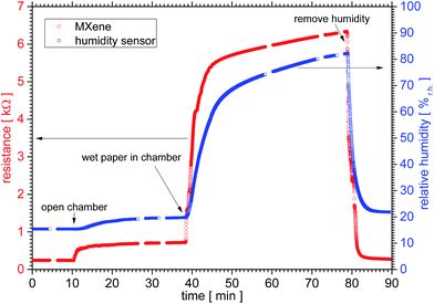
When discussing MXene conductivity the surrounding humidity has to be taken into account, as Dillon et al.26 have shown recently. The effect of humidity on the resistivity is shown in Fig. 5. The resistance changes when the environment is changed from dry nitrogen (N2) to a relative humidity of 80 ± 5%r.h. by a factor of 26, namely from 243 Ω to 6341 Ω. The value is reversible – with a hysteresis smaller than the one of the commercial sensor described above.For the analysis in Fig. 6 we chose data points at around t = 9, 36, 50 and 75 min of Fig. 5, which represent constant values of both curves. A linear fit of y = −(1.2 ± 0.3) kΩ + (0.094 ± 0.004) kΩ/%r.h. × x describes the resistivity vs. relative humidity reasonably well.
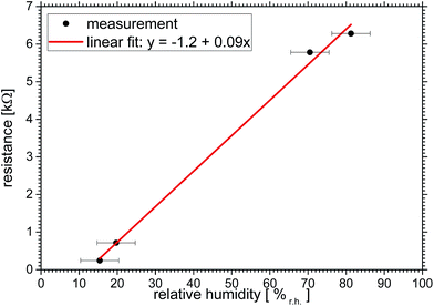 | ||
| Fig. 6 Effect of relative humidity on MXene film resistance for some select data points taken from Fig. 5 at around t = 9, 36, 50 and 75 min. | ||
4 Discussion
We show that the plasma treatment results in a change of 18% in the resistivity by reducing or oxidizing the sample. At P ≤ 20 W, the change is reversible, while at higher power the changes become, to some degree, irreversible. The XPS measurements show an irreversible behaviour, which does not reflect the observed resistivity changes. This is not too surprising since XPS only measures changes in the uppermost layers of the MXene film – that by its very nature is the most susceptible to oxidation – while the conductivity measurements reflect changes across the entire film.The power dependence and the fact, that two different vacuum systems were used for the XPS and resistivity measurements, may explain this deviation since the plasma conditions may not have been identical. The XPS-chamber used a capacitive plasma, while the resistivity measurements were performed using an inductive plasma. The plasma excitation can be different at nominal identical powers and the vacuum system's geometry can also play a significant role.
Regarding the humidity sensor we would like to note that at nominally identical situations the MXene and commercial sensor show different values for two cases: in the beginning at t = 0 min under high vacuum condition the commercial sensor shows 15%r.h. and the MXene 0.243 kΩ respectively. At the end, again under high vacuum and after beeing exposed several times to a humid environment for t = 90 min, the values are 22%r.h. and 0.276 kΩ respectively. Although we did not measure it, we expect that after a long time both – commercial sensor and MXene film – would reach the original values ρ(t = 0 min). This is after 90 min not the case yet. Note that while the deviation from the initial conditions for the commercial sensor is 42%, the MXene's is only 13%. This suggests that at least under these conditions, the MXene film is a faster sensor.
That may be due to the fact that it is – compared to the MXenes – bulk like and moisture needs to diffuse through more material than in the 13 nm thick MXene film.
The linear behaviour of the MXene sensor has been shown within the error bar of 5%r.h. of the commercial sensor. Note that we expect flattening of the curves in Fig. 5 at low and especially high humidities. And while important this is beyond the scope of this paper. The origin of the changed resistivity due to humidity treatment could have the following reasons: the resistivity of the water itself influences the measurement, the macroscopic structure of the flakes is changed or the water reacts with the sample. Due to the MXene's relative chemical stability and the reversibility of the process we neglect the latter.
In the first case, water as a bad conductor may cover the sample. Using Kirchhoff's law, the resistivity should decrease or stay unchanged. The more likely effect, however, is that moisture is captured between the flakes reducing the interparticle contacts that in turn reduces the overall conductivity.
In summary we measured the changes in transport properties of thin spin-cast, 13 nm Ti3C2Tx films as a function of plasma treatments and humidity. The results of this work are:
(1) It is possible to reversibly decrease the resistivity of our films by treating them with H-plasmas and increase it with O-plasmas. The changes with plasma treatment suggests a method to enhance the conductivity of these transparent, temperature stable and printable electrodes.
(2) By changing the humidity from that of dry N2 to 80%r.h., the resistivity changed by a factor of 26. The response time of our films also appears to be somewhat faster than the commercial humidity sensor used herein. Our dynamic range – especially on the low humidity side – also appears to be strongly enhanced.
The ease by which these films can be made is an advantage over more sophisticated humidity sensors.48 For example, the fact that our films can be readily printed renders them compatible with chip technology. Further, the direct change in resistivity may be useful for the low cost self-regulation of humidity in myriad applications. Before these applications can be realized, however, it is important to understand the long-term stability of these films, especially when continually exposed to humid air.
The Ti3C2Tx films change their resistances when exposed to reactive H or O plasmas. They can thus, in principle, be used as H or O sensors. The resistivity of the MXene films was decreased by 18% by H plasma treatment in this very first experiment. In general it opens the route to increase the conductivity of these transparent, temperature stable and printable electrodes.
When taking both effects, humidity and reactives gases, into account, it is likely that the resistivity stems mainly from the overlapping areas of the flakes and not from the chemical structure itself. Therefore the irreversible chemical structure of the MXenes plays a subordinate role, but a reversible change in the termination appears to highly influence the conductivity. In other words, the resistivity seems to be controlled by the interfaces of the overlapping MXene flakes. To get a better insight into this we will investigate single flakes in the future.
5 Conclusion
For a 13 ± 1 nm thick spin-coated layer of two the dimensional Ti3C2 MXene flakes, we find a controllable change of 18 ± 1% in conductivity by selective O and H plasma treatment, rendering these structures interesting candidates for transparent H or O gas sensors. Secondly, a strong dependence of 2610 ± 10% on the relative humidity is observed which renders these transparent 2D flakes low cost and robust materials for miniaturized humidity sensors in, for example, food monitoring.Acknowledgements
We would like to thank L. Schulte-Zweckel, Merve Alyazjie and Fangzhou Wang for assistance in the measurements.References
- M. Xu, T. Liang, M. Shi and H. Chen, Chem. Rev., 2013, 113, 3766–3798 CrossRef CAS PubMed.
- K. S. Novoselov, A. K. Geim, S. V. Morozov, D. Jiang, Y. Zhang, S. V. Dubonos, I. V. Grigorieva and A. A. Firsov, Science, 2004, 306, 666–669 CrossRef CAS PubMed.
- Y. Liu, X. Dong and P. Chen, Chem. Soc. Rev., 2012, 41, 2283–2307 RSC.
- X. Huang, Z. Zeng and H. Zhang, Chem. Soc. Rev., 2013, 42, 1934–1946 RSC.
- Y. Shao, J. Wang, H. Wu, J. Liu, I. A. Aksay and Y. Lin, Electroanalysis, 2010, 22, 1027–1036 CrossRef CAS.
- H. Xu, H. Dai and G. Chen, Talanta, 2010, 81, 334–338 CrossRef CAS PubMed.
- Y. Wang, Y. Shao, D. W. Matson, J. Li and Y. Lin, ACS Nano, 2010, 4, 1790–1798 CrossRef CAS PubMed.
- B. Su, J. Tang, J. Huang, H. Yang, B. Qiu, G. Chen and D. Tang, Electroanalysis, 2010, 22, 2720–2728 CrossRef CAS.
- F. Schedin, A. K. Geim, S. V. Morozov, E. W. Hill, P. Blake, M. I. Katsnelson and K. S. Novoselov, Nat. Mater., 2007, 6, 652–655 CrossRef CAS PubMed.
- T. V. Cuong, V. H. Pham, J. S. Chung, E. W. Shin, D. H. Yoo, S. H. Hahn, J. S. Huh, G. H. Rue, E. J. Kim, S. H. Hur and P. A. Kohl, Mater. Lett., 2010, 64, 2479–2482 CrossRef CAS.
- W. Wu, Z. Liu, L. A. Jauregui, Q. Yu, R. Pillai, H. Cao, J. Bao, Y. P. Chen and S.-S. Pei, Sens. Actuators, B, 2010, 150, 296–300 CrossRef CAS.
- G. Lu, K. Yu, L. E. Ocola and J. Chen, Chem. Commun., 2011, 47, 7761–7763 RSC.
- M. Pumera and A. H. Loo, TrAC, Trends Anal. Chem., 2014, 61, 49–53 CrossRef CAS.
- Q. H. Wang, K. Kalantar-Zadeh, A. Kis, J. N. Coleman and M. S. Strano, Nat. Nanotechnol., 2012, 7, 699–712 CrossRef CAS PubMed.
- H. Li, Z. Yin, Q. He, H. Li, X. Huang, G. Lu, D. W. H. Fam, A. I. Y. Tok, Q. Zhang and H. Zhang, Small, 2012, 8, 63–67 CrossRef CAS PubMed.
- Q. He, Z. Zeng, Z. Yin, H. Li, S. Wu, X. Huang and H. Zhang, Small, 2012, 8, 2994–2999 CrossRef CAS PubMed.
- J. Feng, L. Peng, C. Wu, X. Sun, S. Hu, C. Lin, J. Dai, J. Yang and Y. Xie, Adv. Mater., 2012, 24, 1969–1974 CrossRef CAS PubMed.
- Z. Liu, S. P. Lau and F. Yan, Chem. Soc. Rev., 2015, 44, 5638–5679 RSC.
- M. Naguib, V. N. Mochalin, M. W. Barsoum and Y. Gogotsi, Adv. Mater., 2014, 26, 992–1005 CrossRef CAS PubMed.
- M. W. Barsoum, MAX Phases – Properties of Machinable Ternary, Wiley-VCH, 2013 Search PubMed.
- M. Naguib, M. Kurtoglu, V. Presser, J. Lu, J. Niu, M. Heon, L. Hultman, Y. Gogotsi and M. W. Barsoum, Adv. Mater., 2011, 23, 4248–4253 CrossRef CAS PubMed.
- J. Halim, S. Kota, M. R. Lukatskaya, M. Naguib, M.-Q. Zhao, E. J. Moon, J. Pitock, J. Nanda, S. J. May, Y. Gogotsi and M. W. Barsoum, Adv. Funct. Mater., 2016, 26, 3118–3127 CrossRef CAS.
- J. Halim, K. M. Cook, M. Naguib, P. Eklund, Y. Gogotsi, J. Rosen and M. W. Barsoum, Appl. Surf. Sci., 2016, 362, 406–417 CrossRef CAS.
- J. Halim, M. R. Lukatskaya, K. M. Cook, J. Lu, C. R. Smith, L.-A. Näslund, S. J. May, L. Hultman, Y. Gogotsi, P. Eklund and M. W. Barsoum, Chem. Mater., 2014, 26, 2374–2381 CrossRef CAS PubMed.
- K. Hantanasirisakul, M.-Q. Zhao, P. Urbankowski, J. Halim, B. Anasori, S. Kota, C. E. Ren, M. W. Barsoum and Y. Gogotsi, Adv. Electron. Mater., 2016, 2, 1600050 CrossRef.
- A. D. Dillon, M. J. Ghidiu, A. L. Krick, J. Griggs, S. J. May, Y. Gogotsi, M. W. Barsoum and A. T. Fafarman, Adv. Funct. Mater., 2016, 26, 4162–4168 CrossRef CAS.
- A. Ali, A. Belaidi, S. Ali, M. I. Helal and K. A. Mahmoud, J. Mater. Sci.: Mater. Electron., 2016, 27, 5440–5445 CrossRef CAS.
- Y. Xie, M. Naguib, V. N. Mochalin, M. W. Barsoum, Y. Gogotsi, X. Yu, K.-W. Nam, X.-Q. Yang, A. I. Kolesnikov and P. R. C. Kent, J. Am. Chem. Soc., 2014, 136, 6385–6394 CrossRef CAS PubMed.
- X. Liang, A. Garsuch and L. F. Nazar, Angew. Chem., Int. Ed., 2015, 54, 3907–3911 CrossRef CAS PubMed.
- D. Er, J. Li, M. Naguib, Y. Gogotsi and V. B. Shenoy, ACS Appl. Mater. Interfaces, 2014, 6, 11173–11179 CAS.
- M. R. Lukatskaya, O. Mashtalir, C. E. Ren, Y. Dall'Agnese, P. Rozier, P. L. Taberna, M. Naguib, P. Simon, M. W. Barsoum and Y. Gogotsi, Science, 2013, 341, 1502–1505 CrossRef CAS PubMed.
- M. Ghidiu, M. Lukatskaya, M.-Q. Zhao, Y. Gogotsi and M. Barsoum, Nature, 2015, 516, 78–81 Search PubMed.
- X. Xie, S. Chen, W. Ding, Y. Nie and Z. Wei, Chem. Commun., 2013, 49, 10112–10114 RSC.
- O. Mashtalir, K. M. Cook, V. N. Mochalin, M. Crowe, M. W. Barsoum and Y. Gogotsi, J. Mater. Chem. A, 2014, 2, 14334–14338 CAS.
- Q. Peng, J. Guo, Q. Zhang, J. Xiang, B. Liu, A. Zhou, R. Liu and Y. Tian, J. Am. Chem. Soc., 2014, 136, 4113–4116 CrossRef CAS PubMed.
- A. Miranda, J. Halim, M. W. Barsoum and A. Lorke, Appl. Phys. Lett., 2016, 108, 033102 CrossRef.
- F. Wang, C. Yang, C. Duan, D. Xiao, Y. Tang and J. Zhu, J. Electrochem. Soc., 2015, 162, B16–B21 CrossRef CAS.
- F. Wang, C. Yang, M. Duan, Y. Tang and J. Zhu, Biosens. Bioelectron., 2015, 74, 1022–1028 CrossRef CAS PubMed.
- B. Xu, M. Zhu, W. Zhang, X. Zhen, Z. Pei, Q. Xue, C. Zhi and P. Shi, Adv. Mater., 2016, 28, 3333–3339 CrossRef CAS PubMed.
- X.-F. Yu, Y. chun Li, J. bo Cheng, Z. bo Liu, Q. zhong Li, W. zuo Li, X. Yang and B. Xiao, ACS Appl. Mater. Interfaces, 2015, 7, 13707–13713 CAS.
- B. Xiao, Y. chun Li, X. fang Yu and J. bo Cheng, Sens. Actuators, B, 2016, 235, 103–109 CrossRef CAS.
- M. Ghidiu, J. Halim, S. Kota, D. Bish, Y. Gogotsi and M. W. Barsoum, Chem. Mater., 2016, 28, 3507–3514 CrossRef CAS.
- F. M. Römer, Ph.D. thesis, Universität Duisburg-Essen, 2012.
- F. M. Römer, M. Möller, K. Wagner, L. Gathmann, R. Narkowicz, H. Zähres, B. R. Salles, P. Torelli, R. Meckenstock, J. Lindner and M. Farle, Appl. Phys. Lett., 2012, 100, 092402 CrossRef.
- C. Antoniak, M. E. Gruner, M. Spasova, A. V. Trunova, F. M. Römer, A. Warland, B. Krumme, K. Fauth, S. Sun, P. Entel, M. Farle and H. Wende, Nat. Commun., 2011, 2, 528 CrossRef PubMed.
- U. Wiedwald, K. Fauth, M. Heßler, H.-G. Boyen, F. Weigl, M. Hilgendorff, M. Giersig, G. Schütz, P. Ziemann and M. Farle, ChemPhysChem, 2005, 6, 2522–2526 CrossRef CAS PubMed.
- A. V. Naumkin, A. Kraut-Vass, S. W. Gaarenstroom and C. J. Powell, NIST X-ray Photoelectron Spectroscopy Database V4.1, 2012, http://srdata.nist.gov/xps/ Search PubMed.
- P. Faia, C. Furtado and A. Ferreira, Sens. Actuators, B, 2005, 107, 353–359 CrossRef CAS.
Footnotes |
| † Mesh hole diameter 44 μm, Sandvik™, Sweden. |
| ‡ Alfa Aesar™, 99.5% purity. |
| § Fisher™ TraceMetal grade. |
| ¶ Measured by MKS™ PR 4000. |
| || Leybold™ Turbovac SL80. |
| ** Hüttinger™ PFG 300 RF. |
| †† Keithley™ 2000 multimeter. |
| ‡‡ SPECS™ XRC1000. |
| §§ Conrad Electronics™ HMZ-333A1. |
| This journal is © The Royal Society of Chemistry 2017 |

