
 Open Access Article
 This Open Access Article is licensed under a Creative Commons Attribution-Non Commercial 3.0 Unported Licence
A biomolecule-assisted, cost-efficient route for growing tunable CuInS2 films for green energy application†
Anna Frank‡
a,
Angela S. Wochnik‡b,
Thomas Beinb and
Christina Scheu *ac
*ac
aMax-Planck-Institut für Eisenforschung GmbH, Max-Planck-Straße 1, 40237 Düsseldorf, Germany. E-mail: scheu@mpie.de
bDepartment of Chemistry, Center for NanoScience (CeNS), Ludwig-Maximilians-Universität, Butenandtstrasse 5-11 (E), Munich, Germany
cMaterials Analytics, RWTH Aachen University, Kopernikusstr 10, 52074 Aachen, Germany
First published on 6th April 2017
Abstract
CuInS2 has become a popular and promising candidate as an absorber material in photovoltaic devices and photo-electrochemical cells. Here we report the successful L-cysteine-assisted growth of homogeneous, nanostructured CuInS2 thin films deposited on fluorine-doped tin oxide coated glass. In contrast to existing synthesis routes using thioacetamide as a sulfur source, our method offers the advantage of being environmentally friendly and non-toxic. We found that L-cysteine is able to reduce the Cu2+ ions of the precursor CuSO4 to Cu+ in aqueous solution, thus enabling the formation of CuInS2 thin films. By varying the concentration of the reaction solution during the solvothermal synthesis route, we obtained CuInS2 films with different thicknesses and compositions, investigated with the help of energy dispersive X-ray spectroscopy with scanning and transmission electron microscopy. X-ray and electron diffraction experiments of the films prove the synthesis of a pure CuInS2 phase with the chalcopyrite structure except for the highest L-cysteine concentration where additional In2S3 forms. UV-Vis absorption spectroscopy reveals absorption over the whole visible spectrum. The calculated band gap using the UV-Vis data ranges between 1.4 and 1.5 eV, and can be adjusted by changing crystal size and chemical composition. This offers a promising route towards tuning the optical and transport properties. First dye degradation experiments show promising activity under solar illumination.
Introduction
In recent years, the development of alternative semiconductor materials for photophysical and photochemical applications such as solar cells and solar-driven hydrogen production has become a very active research field. The requirements for these materials include (cost-) efficient manufacturing processes, as well as low toxicity of the synthesis and the material itself. These features can be found in copper indium disulfide (CuInS2), which became one of the most popular and promising candidates for absorber materials in photovoltaic and photochemical applications. Advantages of this material include its good long-term stability, a high absorption coefficient (α ≈ 105 cm−1) and a direct band gap of 1.5 eV.1 Compared to the commonly used CuInSe2, it is not toxic2 and has a high chemical stability.3 Furthermore, the type of conductivity can be tuned depending on the chemical composition.4 Known manufacturing processes include chemical vapor deposition,5 spray pyrolysis6 and electro-deposition.7 However, these methods are rather expensive. Therefore, synthesis of CuInS2 films via cost-efficient methods such as chemical bath deposition,8 successive ionic layer deposition,9 microwave assisted growth,10 hot-injection,11 sol–gel methods12 and mild solvothermal synthesis routes13,14 has attracted increasing attention. In previous reports,15,16 we have presented the synthesis of CuInS2 thin films and microspheres using a one-step, cost-efficient solvothermal method that had been developed by Peng et al.13 and further modified in our studies. This method makes it possible to directly grow thin films on a suitable substrate without the need to deposit the material after synthesis. Depending on the reagent stoichiometry and thermal treatments, we were able to synthesize CuInS2 films with different thicknesses and morphologies, using thioacetamide as the sulfur source.15,16 However, thioacetamide is a toxic and carcinogenic substance. Hence, to prepare CuInS2 thin films via a non-toxic route, we changed the sulfur source to the biomolecule L-cysteine, an amino acid.Biomolecule-assisted synthesis has proven to be a novel, environmentally friendly and promising method to prepare various nanomaterials, making use of the unique features of biomolecules including the capability to engage in self-assembly processes.17 Biomaterials such as DNA, (poly)peptides and amino acids have been used to control the size and shape of various nanomaterials.18–20 L-Cysteine [Cys, HSCH2CH(NH2)COOH] is a thiol-containing amino acid that is inexpensive and environmentally friendly. Additionally, it has a strong affinity towards metal ions to form metal–ligand complexes and can therefore not only act as sulfur source but also as structure directing agent in the synthesis of (not only) sulfidic nanocrystals.20–22 Previously reported L-cysteine-assisted synthesis strategies involving solvothermal processes include Bi2S3, In2S3, CuS, PbS, AgBiS2, TiO2, ZnIn2S4, Cu2CoSnS4 and CuInS2 nanocrystals.17,23–31
CuInS2 nanocrystals have been synthesized by Liu et al. via a L-cysteine-assisted solvothermal process.17 They obtained a product containing agglomerations of irregular microspheres and nanocrystals. Wen et al.31 produced CuInS2 powders using L-cysteine as sulfur source. The powders consisted of microspheres made up of nanosheets. To the best of our knowledge, there have been no reports on the direct growth of CuInS2 thin films on transparent, conductive substrates using L-cysteine as the sulfur source. The electrodes fabricated in this way are of interest for application in photoelectrochemical and solar cells.
Herein we report about a solvothermal synthesis strategy that allows for preparing CuInS2 films directly on fluorine-doped tin oxide (FTO) conductive glass substrates by involving the non-toxic biomolecule L-cysteine. This method enabled us to achieve homogeneous coverage of the FTO substrate, which is a prerequisite for photovoltaic and photoelectrochemical applications. Moreover, the concentration of reactants can be varied to control not only the thickness but also the composition and grain size which directly affect the optical and electrical properties.
Experimental section
Synthesis of CuInS2 films
All reagents were of analytical grade and were used without further purification. FTO conductive glass (Sigma-Aldrich) with dimensions of 15 × 20 × 2 mm was used as substrate for the deposition of the CuInS2 films. All substrates were washed before use in dilute nitric acid, double-distilled water, acetone and ethanol in an ultrasonic cleaner for 5 min respectively. Peng et al.13 dissolved CuSO4·5H2O, InCl3·4H2O and thioacetamide in ethanol and stirred it for 15 min. Afterwards, they placed an FTO substrate in a Teflon-lined stainless steel autoclave and kept it in an oven for 12 h at 160 °C. This procedure was modified in our previous work and a lower temperature was found to be sufficient.15,16 In the present work we changed the sulfur source from thioacetamide to L-cysteine. Three films were prepared using different concentrations of reactants, hereafter referred to as films A, B and C (see Table 1).| CuSO4·5H2O | InCl3 | L-Cysteine | ||
|---|---|---|---|---|
| Film A | Mass [g] | 0.075 | 0.066 | 0.145 |
| Amount [mol] | 0.3 | 0.3 | 1.2 | |
| Molarity [M] | 0.03 | 0.03 | 0.12 | |
| Normalized | 1 | 1 | 4 | |
| Film B | Mass [g] | 0.050 | 0.044 | 0.061 |
| Amount [mol] | 0.2 | 0.2 | 0.5 | |
| Molarity [M] | 0.02 | 0.02 | 0.05 | |
| Normalized | 1 | 1 | 2.5 | |
| Film C | Mass [g] | 0.025 | 0.022 | 0.036 |
| Amount [mol] | 0.1 | 0.1 | 0.3 | |
| Molarity [M] | 0.01 | 0.01 | 0.03 | |
| Normalized | 1 | 1 | 3 | |
In a Teflon liner (20 ml capacity), CuSO4·5H2O and InCl3 were dissolved in 10 ml ethanol and stirred for 10 min. Subsequently, L-cysteine was added and the reaction solution was stirred for another 5 min, resulting in a pH of the reaction solution of around 5, which is the isoelectric point of L-cysteine. For the different reactant concentrations see Table 1. The cleaned FTO substrates were placed in the Teflon liner and the sealed stainless-steel autoclave was heated to 150 °C and kept at this temperature for 18 h. After the reaction the autoclave was left to cool down to room temperature, the obtained films were washed using ethanol and double-distilled water, and dried with compressed air. Samples were stored at ambient conditions.
To investigate whether L-cysteine can reduce Cu2+ to Cu+, the precursors CuSO4·5H2O and L-cysteine were brought to reaction in 10 ml ethanol for 18 h at RT. The resulting grey solid was filtered and washed with ethanol, double-distilled water and dried in air. For comparison, CuSO4·5H2O and L-cysteine were also heated to 150 °C and hold at this temperature for 18 h, following a procedure from Li et al.25
Characterization
The crystal structure of the films was determined by X-ray diffraction (XRD) acquired with a diffractometer of a Seifert Type ID3003 X-ray generator, equipped with a scintillation counter, using Co Kα radiation and an Fe-filter (λ = 1.79 Å). The scanning rate was 0.05° s−1 with a count time of 30 s per step and a 2θ range from 20 to 130°. The obtained patterns were compared to literature data (see ESI Table 1†). Average crystallite size was calculated using the Scherrer equation.32 For this purpose the (112) and (204) peaks were fitted by using a Gaussian function.The morphology was investigated by scanning electron microscopy (SEM) using a ZEISS Merlin operated at 5.0 kV and a probe current of 2.0 nA. Secondary electron (SE) imaging was done using the attached InLens® ZEISS standard detector. The samples were palladium/gold coated prior to the insertion into the SEM. The average chemical composition was analyzed by energy dispersive X-ray (EDX) spectroscopy using the XFlash detector 6|30 from Bruker. EDX was performed at 20.0 kV and a probe current of 4.0 nA. Analysis was done with the Bruker Esprit 1.9.4.5 software and the obtained atomic ratios were normalized relative to copper. Cross sections were prepared for the investigation of the film thickness and images were taken with a focused ion beam (FIB) FEI Helios Nanolab 600. For cutting the samples via FIB, the samples were coated with conductive silver paint to avoid destruction of the sample surface.
For further characterization, (scanning) transmission electron microscopy ((S)TEM) investigations were performed. These were done on an FEI Titan Themis 300 (S)TEM microscope operated at an acceleration voltage of 300 kV and equipped with a CS probe corrector, a Gatan Quantum ERS image filter and a Super X-EDX detector from Bruker. Electron diffraction data were evaluated using a calibrated camera constant obtained from a Si standard. Dual electron energy loss spectroscopy (EELS) was also performed at the FEI Titan Themis using a dispersion of 0.1 eV per channel and an acceleration voltage of 60 kV. This allowed us to study the S-L2,3 edge at around 165 eV and the Cu-L2,3 edge at around 930 eV with a sufficient signal-to-noise ratio.
UV-Vis absorption measurements of the films were done on a Perkin Elmer Lambda 1050 in transmission mode within a spectral region of 250 to 1200 nm (step size 1 nm). The band gap was determined from the UV-Vis data using the Tauc method for direct band gap semiconductors.33 UV-Vis measurements for dye degradation experiments have been performed on a Perkin Elmer Lambda 800 in absorption mode in a range from 260 to 900 nm (also with a step size of 1 nm). Dye degradation has been studied using the dye rhodamine B, solved in water, and under illumination with one sun using a solar simulator.
Results
Fig. 1 shows SE images of the three films synthesized with different concentrations of reactants but using the same reaction temperature and time (150 °C for 18 h). For all films the ratio between Cu and In was 1![[thin space (1/6-em)]](https://www.rsc.org/images/entities/char_2009.gif) :1. For film A the highest amount of sulfur was used to investigate the influence of sulfur. The molar amount of the other precursors was adjusted. For film B and C the same sulfur to copper/indium ratio was used (within the measurement accuracy). The amount of the precursors was doubled for film B compared to film C which should result in different thicknesses of the films. All films grow homogeneously on the FTO substrate and cover it completely. No cracks or delamination of the film could be observed.
:1. For film A the highest amount of sulfur was used to investigate the influence of sulfur. The molar amount of the other precursors was adjusted. For film B and C the same sulfur to copper/indium ratio was used (within the measurement accuracy). The amount of the precursors was doubled for film B compared to film C which should result in different thicknesses of the films. All films grow homogeneously on the FTO substrate and cover it completely. No cracks or delamination of the film could be observed.
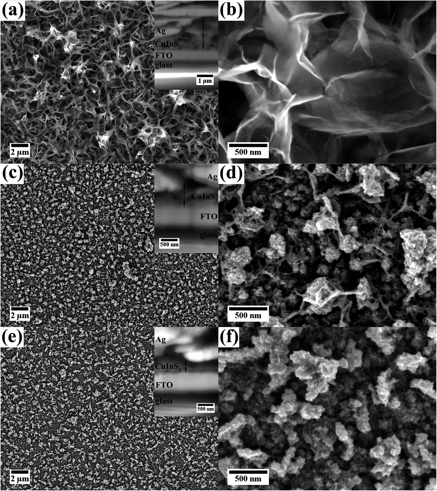 | ||
| Fig. 1 Top view SE images of three CuInS2 films synthesized with different concentrations of reactants on FTO substrates at different magnifications. Images (a) and (b) show film A. Images (c) and (d) are taken from film B. Images (e) and (f) display film C. FIB cross sections of the different films are shown as insets in (a), (c) and (e). | ||
Film A, which exhibits a dark brown color, was synthesized with the highest concentration of 0.03:0.03:0.12 M Cu:In:S and the highest sulfur content, at a nominal Cu:In:S precursor ratio of 1:1:4 (Fig. 1(a) and (b)). The top layer of the film consists of nanoplates. At higher magnification (Fig. 1(b)) the thin, plate-like structures are better visible. The cross-sectional SE image and the TEM investigations described below reveal the presence of a compact layer in contact to the FTO substrate. The underlying FTO substrate cannot be observed in top view indicating that the CuInS2 is completely covering the substrate. The complete film shows a thickness of up to 1.6 μm with partly thinner parts due to varying dimensions of the nanoplates.
SEM images of film B, which displays a brown color, are presented in Fig. 1(c) and (d). This film was synthesized with a lower precursor concentration than film A (only 0.02:0.02:0.05 M) and a nominal precursor ratio of Cu:In:S 1:1:2.5. The film consists of a more dense film with agglomerates on top, which are more loosely packed. Fig. 1(d) (taken at higher magnification) reveals that the film is built up of small CuInS2 nanoparticles. As for film A thin, plate-like structures are visible, although not as pronounced. The thin plates seem to connect the agglomerates. The thickness of the film is around 450 nm with thicker parts due to agglomerates on the surface (up to 700 nm).
Film C has a bright brown color and was synthesized with the lowest concentration of precursors (0.01:0.01:0.03 M, Cu:In:S 1:1:3). This film possesses a surface structure similar to film B, but contains less large agglomerates on top of the film which consist, close to the substrate, of small nanoparticles (Fig. 1(e) and (f)). Thin plate-like features, as for film A and B, cannot be observed. The film thickness is estimated to be around 350 nm with agglomerates sized up to 500 nm.
Comparing the three films, it becomes clear that the molarity of the precursors strongly affects the thickness of the film. The S content of the precursor solution has an influence on the morphology.
The average chemical composition of the films was measured using EDX in SEM. The spectra of all films reveal signals of Cu, In, and S and weaker signals of Sn, Si and O. The detected Sn originates from the FTO substrate and the Si from the glass. The oxygen can stem from FTO or glass. No additional peaks indicating impurities were observed. The appearance of Sn, O and Si signals and the small thickness of the films lead to significant errors in quantification. In addition, the In L and Sn L X-ray energies overlap (see ESI Fig. 1†) which leads to difficulties in the quantification. For this reason EDX measurements have been performed in the STEM where the influence of the FTO substrate leading to the Sn signal can be neglected. SEM EDX quantification results of the films A, B and C are summarized in ESI Table 2.†
The crystal structure of the films was investigated on a global scale via XRD. The XRD patterns of the films possess the characteristic reflections of CuInS2 in the chalcopyrite structure (Fig. 2). Chalcopyrite is a tetragonal crystal structure with lattice parameters a = 0.552 nm and c = 1.112 nm. The observed CuInS2 reflections and all additional reflections originating from the FTO substrate are marked in the pattern (ESI Table 1†). As can be seen, the intensity of the CuInS2 peaks of film A is higher than for film B and C, in accordance with the greater thickness of the film.
 | ||
| Fig. 2 XRD patterns of film A, B and C reveal the tetragonal chalcopyrite crystal structure (*). Additional peaks result from the FTO substrate (#). In case of film A reflections originating from In2S3 are observed (+). | ||
For film A (highest overall concentration as well as highest sulfur content) a few additional reflections, compared to the pattern of film B and C, can be observed. Particularly, there are peaks at around 34.2°, 55.6° and 59.2°. These reflections can arise from CuInS2 in the wurtzite modification ((101) at 34.2° and (103) at 59.2°) or from In2S3, which crystallizes in a distorted tetragonal crystal structure ((206) at 34.2°, (2 2 12) at 55.6° and (329) at 59.2°). The used literature data are summarized in ESI Table 1.† Other possible reflections of these phases overlap either by the chalcopyrite peaks or the peaks arising from the FTO substrate. Coexistence of chalcopyrite and wurtzite modifications of CuInS2 has been observed before.16,34 However, due to the TEM results described below we exclude the presence of CuInS2 in wurtzite crystal structure and attribute the additional peaks to the presence of In2S3. In2S3 thin films, also prepared solvothermally on FTO substrates, have a very similar appearance compared to the surface structure of our film A.35 For the XRD patterns of film B and C the mentioned peaks are not present.
Other byproducts or impurities such as copper sulfides or their oxides were not observed. However, their presence cannot be fully excluded because of the low intensity of the CuInS2 reflections compared to the strong signals of the highly crystalline FTO substrate and the rather broad peaks for CuInS2 due to the small size of the crystals. Beside this all the phases show very similar d-values and can therefore lead to overlapping peaks.
The CuInS2 peaks are rather broad, indicating that small domain or crystal sizes occur in the film structures. These were analyzed by applying the Scherrer equation using a K shape factor of 0.9 for the most intense CuInS2 peaks (112) and (204).32 Average values were obtained from evaluating both peaks. The calculations resulted in an average crystallite size of 10 nm ± 1 nm for all films. More precise crystal size investigation was done on high-resolution TEM images (see below).
The absorption behavior of the films was studied using UV-Vis spectroscopy. The spectra of film A (line), film B (dashed) and film C (dotted) are given in Fig. 3(a). In all cases, the spectra display absorption over the whole visible spectrum. The highest absorption is obtained for film A, which was synthesized with the highest concentration of precursors and shows the highest film thickness of 1.6 μm. Film B and film C also show significant absorption. Due to similar thickness (in the range of 300–500 nm) they show a similar absorption. In general, the absorbance increases linearly with the film thickness.
 | ||
| Fig. 3 (a) UV-Vis spectra of film A (line), B (dashed) and C (dotted). In (b) an exemplary Tauc plot is shown, indicating a band gap of 1.47 eV for film B. | ||
The band gap was calculated from the UV-Vis data using the Tauc method. As an example, the region of the linear fit is marked in Fig. 3 (b, film B). For film A a band gap of 1.43 eV, for film B 1.47 eV and for film C 1.40 eV was estimated. These values are close but lower than the ones mentioned in the literature for the bulk material as well as those reported for nanostructures.1,36 The reason for our band gaps being smaller might be related to the small crystallite size and a corresponding large number of defects in the crystal structure, as well as to differences in composition. This will be discussed in more detail later.
The Urbach tails, visible in the region of the linear fit, have been observed before for CuInS2; they have been attributed to sub-band gap excitations that are related to the defects in the crystal structure and influenced by the chemical composition.37–39 Our films possess small grains which means that a large number of grain boundaries are present in the films. Therefore we assume that the polycrystalline character and the large number of grain boundaries as well as interfaces are the reason for the observed Urbach tails.
(S)TEM investigations were done for all films to determine layer thickness, crystallite size, local crystal structure and chemical composition at the nanometer scale. To do so, films were removed from the substrate and deposited on holey-carbon coated Au grids. This way an influence of the sample preparation on the measurements, especially EDX, can be excluded. A collection of high-resolution TEM images and diffraction patterns is given in Fig. 4 and 5. EDX analysis of all the films was done in STEM mode with a spot size in the range of 1 nm. Data were collected by acquiring EDX maps at different regions and quantification was done for various areas of these maps.
 | ||
| Fig. 4 TEM images (a), (b) and electron diffraction pattern (c), (d) of the top layer of a sample prepared from film A. The electron diffraction pattern can be indexed according to tetragonal In2S3.40 | ||
 | ||
| Fig. 5 TEM images of the synthesized CuInS2 samples. Panels (a and b), film A. Panels (c and d), film B. Panels (e and f), film C. Panels (a), (c) and (e) show the HRTEM images of the samples of film A, B and C, respectively. Panels (b), (d) and (f) show the related electron diffraction patterns and prove polycrystallinity of the samples. Reflections originating from In2S3 are in italic writing. | ||
In the SEM film A with the highest concentration of precursors (0.03:0.03:0.12 M, nominal Cu:In:S precursor ratio 1:1:4) showed a layer of nanoplates, connected to each other (see Fig. 1). These nanoflakes can also be observed in the TEM (Fig. 4). The TEM images show a more compact part of the film (bottom layer) with outgrowing nanoflakes (surface layer). The flaky structure seems so consists of darker appearing rods with outgrowing flakes. These flakes then interconnect with each other and other rods. While acquiring EDX data it became obvious that the film consists of a Cu rich bottom layer and an In rich surface layer which forms the in the top view SEM observed flakes (an exemplary EDX map is shown in the ESI Fig. 2†). EDX spectra acquired in STEM mode on film A reveal 12 ± 4 at% Cu, 34 ± 3 at% In and 54 ± 4 at% S for the surface layer giving a ratio of 1.0:3.0:4.8. This ratio is drastically deficient in Cu and therefore confirms the presence of In2S3, with some Cu incorporated. In2S3 was also detected by XRD. As mentioned before, In2S3 can be synthesized solvothermally using L-cysteine, resulting in a very similar topology.35 High-resolution TEM images and electron diffraction pattern taken from only a flaky area as well as from an area with both flakes and rods prove the (poly) crystallinity of the surface layer. Considering the EDX measurements which show a very low amount of copper the electron diffraction pattern in Fig. 4(c) and (d) have been indexed according to tetragonal In2S3.40 The coexistence of other phases such as CuInS2 and Cu2S cannot be excluded (for comparison of d-values see ESI Table 1†).
In the STEM EDX measurement the bottom layer of film A gives 22 ± 4 at% Cu, 28 ± 4 at% In and 50 ± 6 at% S, meaning a ratio of 1.0:1.3:2.3 which is close to the stoichiometric ratio of Cu:In:S 1:1:2 but slightly In and S rich. In Fig. 5(a) and (b) a high-resolution TEM image as well as a diffraction pattern of the bottom layer can be found. It becomes clear that the bottom layer of film A is built up of small nanocrystals which agglomerate to form a more compact layer of CuInS2. Single crystallites are exemplarily marked in Fig. 5(a). The average size of the nanoparticles is 6.3 ± 2.6 nm. The electron diffraction pattern (Fig. 5(b)) shows polycrystallinity and can be indexed according to the tetragonal CuInS2 phase with d-values of (112), (204)/(220), (301) and (116)/(312) as well as tetragonal In2S3 and its (200)/(116), (211), (213)/(109), (2 0 14), (329)/(413) and (420)/(336) planes. The presence of CuInS2 in the hexagonal wurtzite modification cannot be excluded ((100), (002), (110), (103) and (112)). Furthermore, as mentioned before Cu(I)-sulfides show similar d-values (see ESI Table 1†) but their presence can be excluded by the EDX measurements. The phase diagram of the (Cu–In–S)-system resulting from a quasi-binary system of Cu2S–In2S3 indicates the predominant formation of CuInS2 in the chalcopyrite structure with around 50 to 52% mole percent In2S3 for the given conditions.41 As we used Cu and In in equimolar composition, we assume that the system is in that region of the phase diagram.
The (S)TEM investigations of film B (medium concentration of precursors, 0.2:0.2:0.5, nominal Cu:In:S precursor ratio 1:1:2.5, Fig. 5(c) and (d)) give similar results as for the bottom layer of film A. They reveal a layer of CuInS2 which consists of agglomerated nanoparticles. Again, high resolution TEM imaging and electron diffraction demonstrate the polycrystallinity of the as-synthesized CuInS2 layer and show no obvious reflections of any side product like Cu or In sulfides. In rich areas as described for film A (surface nanoflake layer) cannot be observed. The average crystallite size is 5.3 ± 2.2 nm. EDX gives 24 ± 2 at% Cu, 25 ± 2 at% In and 51 ± 3 at% S. The Cu:In:S ratio is 1.0:1.0:2.1, which is very close to a stoichiometric composition.
For the lowest concentration of precursors (film C, 0.1:0.1:0.3, nominal Cu:In:S precursor ratio 1:1:3, Fig. 5(e)–(f)) electron diffraction and high resolution TEM show that the film is crystalline, too. For this film the crystal size is 4.9 ± 2.0 nm. The EDX analysis gives 26 ± 2 at% Cu, 24 ± 2 at% In and 51 ± 3 at% S which results in Cu:In:S 1.0:0.9:2.0. As for film B this is also very close to a stoichiometric composition of CuInS2.
However, as already mentioned the presence of other side products like In2S3 or CuI sulfides cannot be fully excluded because of the very similar d-values of the compounds (see ESI Table 1†). Nevertheless, because in the XRD pattern of film B and C no reflections of such byproducts can be found and the EDX measurements show stoichiometric CuInS2 quantification we assume that the presence of In2S3 and Cu2S can be neglected for films B and C.
To investigate the growth mechanism of the films, the reaction of L-cysteine with CuSO4 was analyzed. When L-cysteine and CuSO4 are dissolved in ethanol, a grey solid is formed after stirring for 18 h at room temperature (RT). The XRD pattern reveals many reflections (see Fig. 6(a)). The most intense reflections correspond to crystalline, hexagonal L-cystine (a = 0.54 nm, c = 5.59 nm), which is formed during the reaction between L-cysteine and Cu2+ in the reaction solution (see also Fig. 9 in the Discussion section).25,42 Other reflections match well with a Cu–cysteine complex in a monoclinic crystal structure with the lattice parameters a = 1.41 nm, b = 0.45 nm and c = 0.98 nm as described by Dokken et al.43 Additionally, weak reflections of Cu2S can be found in the XRD spectrum (Fig. 6).44,45 The intense background is due to the presence of an amorphous phase, e.g., non-crystalline Cu cysteine complexes or remaining precursors.
 | ||
| Fig. 6 (a) XRD pattern of the grey reaction product of L-cysteine and CuSO4 stirred for 18 h at RT. The measured pattern is a mixture of crystalline L-cystine42 (marked with *) and Cu–cysteine complexes (marked with #) as published by Dokken et al.46 The presence of hexagonal or tetragonal Cu2S cannot be excluded (marked with ° and +, respectively). (b) XRD pattern of L-cysteine and CuSO4 reacted at 150 °C for 18 h. Every reflection fits well with a hexagonal CuS phase.47 | ||
Furthermore, L-cysteine and CuSO4 were brought to reaction for 18 h at 150 °C. The resulting black powder was also analyzed with XRD, and the pattern shows reflections that all fit well to hexagonal CuS. No additional reflections were observed.
(S)TEM analysis of the grey solid shows 1.5–5 nm sized crystals embedded in an amorphous material. The high-resolution TEM and BF images are given in Fig. 7(a) and (b). The electron diffraction pattern reveals reflections with d values of 3.4 Å, 3.2 Å, 1.9 Å and 1.6 Å and a polycrystalline character of the sample. These values can be assigned to (0 0 −18), (0 2 16)/(0 2 14) and (−1 3 18) of L-cystine and to CuI cysteine complexes, but also to (102), (202)//(114)/(200) and (213) of Cu2S in the tetragonal structure, as well as to the (100)//(102), (110)//(103) and (004) reflections of Cu2S in the hexagonal structure (diffraction pattern shown in Fig. 7(c), the corresponding values are listed in ESI Table 1†). The same reflections were found in the XRD pattern (Fig. 6). CuIIS or CuxO was not observed.
 | ||
| Fig. 7 (a) High resolution TEM image of the reaction product of L-cysteine and CuSO4 in ethanol shows 1.5–5 nm sized crystals (exemplarily marked white) embedded in an amorphous material. (b) BF image shows the investigated agglomerated particles. (c) Diffraction pattern of the agglomerate reveals polycrystallinity of the reaction product. Diffraction rings fit to L-cystine and tetragonal as well as hexagonal Cu2S. | ||
EELS measurements in STEM confirmed the presence of Cu2S or CuI, respectively. The S-L2,3 and Cu-L2,3 edges in the spectra show similarities to the one of Cu2S when compared with data from the literature (Fig. 8).48 For the heated sample, the EELS spectra show characteristics of CuS or CuII, respectively.
 | ||
| Fig. 8 EELS spectra taken from the product of L-cysteine and CuSO4. The obtained S-L2,3 and Cu-L2,3 edges for the product stirred at RT for 18 h (bottom curves, black and blue) indicate the presence of Cu+ when compared with literature.48 The ones taken from the product synthesized for 18 h at 150 °C show differences, which indicate the formation of Cu2+ (upper curves, green and violet) when compared to literature spectra.48 | ||
Discussion
In Table 2 the results for the three synthesized films A, B and C are summarized. For all the films the ratio between Cu and In precursor was fixed at 1:1 while the S content was varied. For film A the highest amount of sulfur was used (the concentration of the other precursors was adjusted), whereas for film B and C only the molarity was changed.
| Film A | Film B | Film C | |
|---|---|---|---|
| Cu:In:S molarity [M] |
0.03:0.03:1.2 |
0.02:0.02:0.05 |
0.01:0.01:0.03 |
| Nominal Cu:In:S precursor ratio |
1:1:4 |
1:1:2.5 |
1:1:3 |
| Film thickness [nm] | 1600 | 450 | 350 |
| Crystallite size XRD [nm] | 10 ± 1 | 10 ± 1 | 10 ± 1 |
| Band gap [eV] | 1.43 | 1.47 | 1.40 |
| Cu:In:S EDX TEM |
1.0:3.0:4.8 |
1.0:1.0:2.1 |
1.0:0.9:2.0 |
| 1.0:1.3:2.3 |
|||
| Crystallite size TEM [nm] | 6.3 ± 2.6 | 5.3 ± 2.2 | 4.9 ± 2.0 |
| Proposed conductivity type | n | p | p |
The different film thicknesses can be explained with the use of different reactant concentrations. For the highest molar concentration of precursors in film A the largest film thickness of 1.6 μm can be obtained. For film B and C with a lower molarity the film thickness is lower. These two films were synthesized with the same sulfur to copper/indium ratio but a higher molarity for film B compared to film C. This results only in a higher thickness for film B compared to C while the morphology of the films stays the same (compact nanoparticle film). Due to the higher amount of sulfur for sample A the surface topography was changed and a surface structure consisting of interconnected nanoflakes was synthesized. By applying the Scherrer equation32 on the obtained XRD pattern an average crystallite size of 10 ± 1 nm was calculated for all the films. However, analysis of the HR-TEM data resulted in smaller crystal sizes. Film A consists of crystals up to 6.3 ± 2.6 nm, film B (with a lower reactant concentration) of crystals up to 5.3 ± 2.2 nm, and for film C an average crystallite size of 4.9 ± 2.0 nm was determined. All crystal sizes are rather similar but it seems that the lower the S content in the precursor solution (film A > film C > film B) the smaller the crystals (film A > film B > film C). Therefore it can be concluded that during the reaction the film starts to grow with CuInS2 nuclei of similar size to form a polycrystalline compact film consisting of small nanoparticles. Dependent on the amount of precursor salts, more or fewer crystals are formed in the reaction solution and as a consequence there are more and larger agglomerates on top of this compact layer for higher precursor concentrations (film B > film C).
It is well known that CuInS2 can be both a p- or an n-type semiconductor dependent on the chemical composition.4 For stoichiometric, Cu-rich as well as S-rich compositions p-type conductivity can be obtained.49,50 Only In-rich CuInS2 shows n-type conductivity.51 The EDX data obtained in STEM mode show slightly higher S content for film B, which should improve the p-type conductivity of CuInS2.49 For film C a small lack of In can be obtained with EDX in STEM which should also lead to an improved p-type conductivity.49,50 Film A has a completely different structure compared to films B and C. (S)TEM showed two distinct layers. For the surface layer, consisting of nanoflakes and rods, EDX revealed mainly the presence of sulfur and indium. This is in accordance to electron diffraction where the formation of In2S3 was also proven. The bottom layer, however, showed a roughly stoichiometric CuInS2 composition with only slightly higher In and S amounts. Higher In amount can lead to n-type semiconductivity in CuInS251 and In2S3 is a known n-type semiconductor.35 The combination of CuInS2 and In2S3 for e.g. solar cells or water splitting is also already known in literature.52,53 The synthesis of both materials at the same time seems to be promising for future applications.
UV-Vis measurements show a close to linear dependence of absorbance on the film thickness. For film A with the highest film thickness of 1.6 μm, the absorbance is fourfold compared to the thinner films B and C, which have a thickness of 300–500 nm. Nevertheless, all the films show significant absorption over the whole visible spectrum, which is a prerequisite for the use in solar-driven applications. Investigations of the band gaps, using the Tauc plot for direct band gap semiconductors, resulted in band gaps close to the value of 1.5 eV for the bulk material.1 The calculated band gaps are 1.43 eV for film A, 1.47 eV for film B and 1.40 eV for film C, respectively. Decreasing of the band gap could be due to the polycrystallinity and related band gap states. Polycrystallinity implies that a large number of defects, e.g. grain boundaries, are present which can lead to sub-band excitations (e.g. Urbach tails, see Fig. 3). In addition, the different chemical composition can affect the band gap values.
To understand the formation of CuInS2 via the L-cysteine assisted solvothermal synthesis in more detail, we performed additional experiments. On the one hand, CuSO4 and L-cysteine were stirred in ethanol for 18 h at RT (ratio Cu:S 1:2.5, molarity 0.02 M:0.05 M), on the other hand the reaction solution was heated to 150 °C for 18 h.
A redox reaction takes place when L-cysteine (the sulfur source) reacts with CuII ions from the aqueous CuSO4 solution to CuI, while the thiols are oxidized to disulfides (L-cystine, see Fig. 9). CuI can interact with the excess thiols. In addition, due to favorable soft-acid/base interactions a CuI cysteine complex can be formed. This mechanism is reported in the literature.25,46,54,55
 | ||
| Fig. 9 Oxidation of L-cysteine to L-cystine. | ||
Li et al.25 synthesized CuS nanoparticles from CuCl2 and L-cysteine by a hydrothermal method (160 °C, 12 h). They used different ratios of L-cysteine to CuCl2 (1:1, 2:1, 3:1) and observed particles with different morphologies (ranging from microspheres to flakes). For the highest ratio of L-cysteine to CuCl2 (3:1) precipitates were formed in the precursor solution after 15 min of stirring at room temperature. Their investigation showed that these precipitates consist of CuI cysteine complexes and cystine. After the redox reaction between L-cysteine and the CuII ions from the precursor salt, which leads to CuI and cystine, complexes are formed which stabilize the CuI. No Cu2+ ions were left after the reaction. During hydrothermal treatment, sulfur is released from L-cysteine and CuI is oxidized.56 Consequently, CuIIS is formed as the product.
Comparing the results from Li et al.25 with our reaction system, we can derive a similar mechanism: when stirring L-cysteine with CuSO4 at a ratio of 2.5:1 for 18 h at room temperature, we observe a grey solid, which consists not only of cystine and CuI and CuII cysteine complexes but also of Cu2S particles. Cu2S particles were formed in our case because of the long stirring and thus beginning decomposition of the S–S bonds of the cystine molecules and release of S from the remaining L-cysteine. Hence, the sample where L-cysteine and CuSO4 in ethanol were heated for 18 h at 150 °C gave only hexagonal CuS (see XRD pattern in Fig. 6(b) and 8).
During the solvothermal CuInS2 synthesis reactions occur similar to those mentioned above. Free In3+ can react with S2−, which stems from the decomposition of L-cysteine and L-cystine, to form dissolved (InS2)−. The latter mechanism has been observed in literature in similar systems.17,31,57 The (InS2)− can react with Cu+ in solution to form the ultimate product CuInS2. The L-cysteine complexes stabilize the CuI until enough sulfur is released from cystine to form (InS2)−, which can react with CuI. After reacting with (InS2)−, CuInS2 is formed. Li et al.25 observed a higher amount of CuII ions in their precursor with a lower L-cysteine to CuCl2 ratio of 2:1. In contrast, we did not found any CuII containing phases. Therefore we can conclude that for our synthesis pathway a ratio of S:Cu of 2.5:1 is already sufficient to suppress the formation of CuIIS phases. Because the S:Cu ratio is higher for all our films (precursor ratio A: 4:1, B: 2.5:1, C: 3:1) this should be true also for the other films.
As already mentioned above, the (Cu–In–S)-system can be described with the help of the quasi-binary Cu2S–In2S3 phase diagram. This phase diagram indicates the formation of mainly CuInS2 in the chalcopyrite structure at around 50 to 52% mole percent In2S3.41 In our reaction we use Cu:In at equimolar composition, so the formation of CuInS2 in the chalcopyrite structure is plausible and can be supported with the XRD and electron diffraction data.
The reason for the morphology of film A with the highest Cu:In:S precursor ratio of 1:1:4 consisting of a compact CuInS2 bottom layer and a flaky In2S3 surface layer is related to the high L-cysteine amount. More L-cysteine means more Cu–cysteine/cystine complexes and therefore less free Cu ions. Due to the high S amount a lot of free S2− ions are available beside the free In3+. The formation of In2S3 out of InCl3 and L-cysteine is reported in literature.35 Interestingly, the here synthesized film has the same appearance as CuInS2 films solvothermally synthesized with thioacetamide as sulfur source.15
Additionally, we note that we only use L-cysteine as reducing species while in literature studies additional reducing agents such as ethylenediamine and N,N-dimethylformamide (DMF) have been added.17,31
As mentioned above, Wen et al.31 synthesized CuInS2 powder with L-cysteine as sulfur source and DMF as a solvent. They obtained microspheres made up of nanosheets with varying sheet thickness from 50 to 100 nm. They proposed that CuII was reduced to CuI by the solvent DMF. Despite using a different Cu source and solvent, a powder with similarly composed nanospheres was obtained during our reaction in addition to the films in the autoclave.
Liu et al.17 also synthesized CuInS2 nanocrystals via an L-cysteine-assisted solvothermal process. Using ethylene diamine:water 1:1 as solvent, a product of agglomerates of irregular microspheres and nanocrystals was obtained. The SEM study of their product shows a structure of nanocrystals similar to the SEM top view of our film B (Fig. 1(d)). XRD data revealed the tetragonal chalcopyrite structure, which was confirmed using electron diffraction patterns obtained in the TEM in accordance to our studies.
To summarize, the solvothermally grown CuInS2 films synthesized in this study show promising properties: suitable band gaps for solar-driven applications, an interesting nanostructure and good crystallinity. First dye degradation tests with the dye rhodamine B show that the films are active under solar illumination (see ESI Fig. 3†).
Conclusion
In this study L-cysteine was used for the first time to prepare CuInS2 thin films on FTO via a cost-efficient solvothermal synthesis route with low toxicity. It is shown that L-cysteine is able to reduce CuII from the used CuSO4 precursor in aqueous solution to CuI to induce the formation of CuInS2. All three resulting CuInS2 films, synthesized with different concentrations of reactants, show different film thicknesses, slightly different grain sizes and vary in chemical composition dependent on the amount of sulfur used. The microstructural investigations reveal a polycrystalline compact layer for all films, except for the film with the highest amount of sulfur which shows an additional surface layer consisting of interconnected nanoflakes. EDX measurements show nearly stoichiometric composition of the films but for the nanoflake layer a drastically In rich composition. This is accordance to electron and X-ray diffraction data which reveal that the flakes crystallize as In2S3 while the compact films show the characteristic reflections of CuInS2 in the chalcopyrite structure. Moreover, all three films A, B and C show significant optical absorption over the whole visible spectrum and offer suitable band gaps for solar energy applications. The band gap value depends on the composition as well as on the grain size. The films are viewed as possible candidates for absorber layers in solar cells or photoelectrochemical cells, especially the combination of CuInS2 and In2S3 can be very interesting. First dye degradation tests under solar illumination show promising activity of the films.Acknowledgements
Financial support from the cluster of excellence Nanosystems Initiative Munich (NIM) is gratefully acknowledged. The authors thank Benjamin Breitbach and Sophia Betzler for technical support.References
- B. Tell, J. L. Shay and H. M. Kasper, Phys. Rev. B: Solid State, 1971, 4, 2463–2471 CrossRef.
- F. M. Courtel, R. W. Paynter, B. Marsan and M. Morin, Chem. Mater., 2009, 21, 3752–3762 CrossRef CAS.
- C.-W. Chen, D.-Y. Wu, Y.-C. Chan, C. C. Lin, P.-H. Chung, M. Hsiao and R.-S. Liu, J. Phys. Chem. C, 2015, 119, 2852–2860 CAS.
- D. C. Look and J. C. Manthuruthil, J. Phys. Chem. Solids, 1976, 37, 173–180 CrossRef CAS.
- J. A. Hollingsworth, K. K. Banger, M. H. C. Jin, J. D. Harris, J. E. Cowen, E. W. Bohannan, J. A. Switzer, W. E. Buhro and A. F. Hepp, Thin Solid Films, 2003, 431–432, 63–67 CrossRef CAS.
- M. C. Zouaghi, T. B. Nasrallah, S. Marsillac, J. C. Bernède and S. Belgacem, Thin Solid Films, 2001, 382, 39–46 CrossRef CAS.
- S. i. Kuranouchi and T. Nakazawa, Sol. Energy Mater. Sol. Cells, 1998, 50, 31–36 CrossRef CAS.
- H. M. Pathan and C. D. Lokhande, Appl. Surf. Sci., 2004, 239, 11–18 CrossRef CAS.
- Y. Shi, Z. Jin, C. Li, H. An and J. Qiu, Appl. Surf. Sci., 2006, 252, 3737–3743 CrossRef CAS.
- H. Liu, C. Gu, W. Xiong and M. Zhang, Sens. Actuators, B, 2015, 209, 670–676 CrossRef CAS.
- J. Guo, G. Chang, W. Zhang, X. Liu and Y. He, Chem. Phys. Lett., 2016, 647, 51–54 CrossRef CAS.
- M. H. Amerioun, M. E. Ghazi, M. Izadifard and B. Bahramian, Eur. Phys. J. Plus, 2016, 131, 1–9 CrossRef CAS.
- S. Peng, F. Cheng, J. Liang, Z. Tao and J. Chen, J. Alloys Compd., 2009, 481, 786–791 CrossRef CAS.
- Y. Zhao, F. Luo, M. Zhuang, Z. Liu, A. Wei and J. Liu, Appl. Phys. A, 2016, 122, 1–7 CrossRef.
- A. Wochnik, C. Heinzl, F. Auras, T. Bein and C. Scheu, J. Mater. Sci., 2012, 47, 1669–1676 CrossRef CAS.
- A. S. Wochnik, A. Frank, C. Heinzl, J. Häusler, J. Schneider, R. Hoffmann, S. Matich and C. Scheu, Solid State Sci., 2013, 26, 23–30 CrossRef CAS.
- H.-T. Liu, J.-S. Zhong, B.-F. Liu, X.-J. Liang, X.-Y. Yang, H.-D. Jin, F. Yang and W.-D. Xiang, Chin. Phys. Lett., 2011, 28, 057702 CrossRef.
- C. F. Monson and A. T. Woolley, Nano Lett., 2003, 3, 359–363 CrossRef CAS.
- Q. Lu, F. Gao and S. Komarneni, J. Am. Chem. Soc., 2003, 126, 54–55 CrossRef PubMed.
- X. Chen, X. Zhang, C. Shi, X. Li and Y. Qian, Solid State Commun., 2005, 134, 613–615 CrossRef CAS.
- M. C. Brelle, J. Z. Zhang, L. Nguyen and R. K. Mehra, J. Phys. Chem. A, 1999, 103, 10194–10201 CrossRef CAS.
- J. Xiang, H. Cao, Q. Wu, S. Zhang, X. Zhang and A. A. R. Watt, J. Phys. Chem. C, 2008, 112, 3580–3584 CAS.
- B. Zhang, X. Ye, W. Hou, Y. Zhao and Y. Xie, J. Phys. Chem. B, 2006, 110, 8978–8985 CrossRef CAS PubMed.
- P. Zhao, T. Huang and K. Huang, J. Phys. Chem. C, 2007, 111, 12890–12897 CAS.
- B. Li, Y. Xie and Y. Xue, J. Phys. Chem. C, 2007, 111, 12181–12187 CAS.
- J. Xiang, H. Cao, Q. Wu, S. Zhang and X. Zhang, Cryst. Growth Des., 2008, 8, 3935–3940 CAS.
- J. Zhong, W. Xiang, C. Xie, X. Liang and X. Xu, Mater. Chem. Phys., 2013, 138, 773–779 CrossRef CAS.
- Y. Tao, N. Cao, J. Pan, Y. Sun, C. Jin and Y. Song, J. Mater. Sci., 2014, 49, 897–904 CrossRef CAS.
- C. Wen, W. Aiwu, R. Tingke, H. Jie, F. Li, Z. Jiasong and X. Weidong, Micro Nano Lett., 2015, 10, 45–49 Search PubMed.
- J. Zhong, Q. Wang and W. Cai, Mater. Lett., 2015, 150, 69–72 CrossRef CAS.
- C. Wen, X. Weidong, W. Juanjuan, W. Xiaoming, Z. Jiasong and L. Lijun, Mater. Lett., 2009, 63, 2495–2498 CrossRef.
- P. Scherrer, Nachr. Ges. Wiss. Goettingen, Math.-Phys. Kl., 1918, 26, 3 Search PubMed.
- J. Tauc and A. Menth, J. Non-Cryst. Solids, 1972, 8–10, 569–585 CrossRef CAS.
- B. Koo, R. N. Patel and B. A. Korgel, Chem. Mater., 2009, 21, 1962–1966 CrossRef CAS.
- L. Zhang, W. Zhang, H. Yang, W. Fu, W. Zhao, H. Zhao and J. Ma, Mater. Chem. Phys., 2011, 130, 932–936 CrossRef CAS.
- M. Benchikhi, R. El Ouatib, L. Er-Rakho and B. Durand, Ceram. Int., 2016, 42, 11303–11308 CrossRef CAS.
- K. Das, S. K. Panda, S. Gorai, P. Mishra and S. Chaudhuri, Mater. Res. Bull., 2008, 43, 2742–2750 CrossRef CAS.
- J. H. Werner, J. Mattheis and U. Rau, Thin Solid Films, 2005, 480–481, 399–409 CrossRef CAS.
- S. Siebentritt, Sol. Energy Mater. Sol. Cells, 2011, 95, 1471–1476 CrossRef CAS.
- A. Lafond, X. Rocquefelte, M. Paris, C. Guillot-Deudon and V. Jouenne, Chem. Mater., 2011, 23, 5168–5176 CrossRef CAS.
- J. J. M. Binsma, L. J. Giling and J. Bloem, J. Cryst. Growth, 1980, 50, 429–436 CrossRef CAS.
- S. A. Moggach, D. R. Allan, S. Parsons, L. Sawyer and J. E. Warren, J. Synchrotron Radiat., 2005, 12, 598–607 CAS.
- K. M. Dokken, J. G. Parsons, J. McClure and J. L. Gardea-Torresdey, Inorg. Chim. Acta, 2009, 362, 395–401 CrossRef CAS.
- P. Lukashev, W. R. L. Lambrecht, T. Kotani and M. van Schilfgaarde, Phys. Rev. B: Condens. Matter Mater. Phys., 2007, 76, 195202 CrossRef.
- A. Janosi, Acta Crystallogr., 1964, 17, 311–312 CrossRef CAS.
- K. M. Dokken, J. G. Parsons, J. McClure and J. L. Gardea-Torresdey, Inorg. Chim. Acta, 2009, 362, 395–401 CrossRef CAS.
- H. Fjellvag, F. Gronvold, S. Stolen, A. F. Andresen, R. Mueller Kaefer and A. Simon, Z. Kristallogr., 1988, 184, 111–121 CrossRef.
- F. Hofer and P. Golob, Ultramicroscopy, 1987, 21, 379–383 CrossRef CAS.
- H. Bihri and M. Abd-Lefdil, Thin Solid Films, 1999, 354, 5–8 CrossRef CAS.
- B. Tell, J. L. Shay and H. M. Kasper, J. Appl. Phys., 1972, 43, 2469–2470 CrossRef CAS.
- N. H. Y. H. J. Hsu, R. S. Tang, T. M. Hsu and H. L. Hwang, J. Cryst. Growth, 1984, 20, 83 Search PubMed.
- T. Theresa John, M. Mathew, C. Sudha Kartha, K. P. Vijayakumar, T. Abe and Y. Kashiwaba, Sol. Energy Mater. Sol. Cells, 2005, 89, 27–36 CrossRef.
- Gunawan, W. Septina, S. Ikeda, T. Harada, T. Minegishi, K. Domen and M. Matsumura, Chem. Commun., 2014, 50, 8941–8943 RSC.
- D. Cavallini, C. De Marco, S. Duprè and G. Rotilio, Arch. Biochem. Biophys., 1969, 130, 354–361 CrossRef CAS PubMed.
- M. Ahmed, M. S. Iqbal, N. Tahir and A. Islam, World Appl. Sci. J., 2011, 14, 210–214 CAS.
- P. Roy and S. K. Srivastava, Cryst. Growth Des., 2006, 6, 1921–1926 CAS.
- A. Kharkwal, S. N. Sharma, K. Jain and A. K. Singh, Mater. Chem. Phys., 2014, 144, 252–262 CrossRef CAS.
Footnotes |
| † Electronic supplementary information (ESI) available. See DOI: 10.1039/c6ra27294k |
| ‡ Contributed equally. |
| This journal is © The Royal Society of Chemistry 2017 |