 Open Access Article
A wearable piezoelectric bending motion sensor for simultaneous detection of bending curvature and speed†
Sung Yun Chunga,
Hwa-Jin Leea,
Tae Il Lee*b and
Youn Sang Kim*ac
aProgram in Nano Science and Technology, Graduate School of Convergence Science and Technology, Seoul National University, Seoul 08826, Republic of Korea. E-mail: younskim@snu.ac.kr
bDepartment of Bio-Nanotechnology, Gachon University, Gyeonggi-do 13120, Republic of Korea. E-mail: t2.lee77@gachon.ac.kr
cAdvanced Institute of Convergence Technology, 145 Gwang gyo-ro, Yeongtong-gu, Suwon-si, Gyeonggi-do 16229, Republic of Korea
First published on 12th January 2017
Abstract
For simultaneous detection of bending curvature and speed, a wearable bending motion sensor was developed by measuring the output voltage signals. A discrepancy in the piezoelectric output voltages was effectively sensed as a function of bending curvature and speed for recognition of bending motions of the piezoelectric element. This simultaneously bending curvature and speed detectable flexible bending motion sensor is superior compared to other piezoelectric sensors which demonstrated a difference in piezoelectric output signals as a function of only bending curvature. For the wearable platform of the device, elastic ZnO NR–PDMS and Ag NW–SWCNT were utilized as active and electrode materials. This wearable and flexible piezoelectric bending motion sensor is expected to be applied toward the realization of artificial skin motion detectors.
Development of flexible and portable bending motion sensors has recently flourished for diverse applications including human artificial skin,1 wearable electronics,2,3 and biomimetic robot systems.4 Among diverse transduction mechanisms for bending sensors such as resistivity,5–10 capacitance change,11 optical power,12,13 and piezoelectric output potential,14,15 piezoelectric potential change is desirable for a self-powered active system as well as the benefits in portability, environmental compatibility, and persistent utilization. Moreover, oxide based wurtzite piezoelectric materials have advantages in flexibility, low cost, and availability for wearable manufacturing.
Sensing of bending curvature and speed in a simultaneous manner enables an accurate tracking of bending motions across the piezoelectric sensor. However, most researches have simply been focused on the change of piezoelectric outputs as a function of bending curvatures.14,15 For instance, piezoelectric sensor demonstrated by Nour et al., which has double-sided ZnO nanowire (NW) configuration, simply presented different output voltages according to only bending curvature.15 However, the generated piezoelectric outputs affected by bending speed as well as the bending curvature.16 More precisely, the piezoelectric bending motion sensor during the same bending curvature operation with different bending speed will have apparent different signal values. Therefore, two factors, bending curvature and speed, need to be considered together in one bending motion for the piezoelectric sensor as experimental conditions. Through this step, bending motions across the piezoelectric sensor are able to be accurately speculated with awareness of the bending curvature and speed.
Herein, the wearable piezoelectric bending motion sensor was demonstrated with simultaneous analysis on bending curvature and speed. To recognize the bending motions, the output voltages and voltage area were presented according to the bending curvature and speed and the correlation between the voltage area and these two factors was analyzed. For bendability, a polydimethylsiloxane (PDMS) sandwiched ZnO nanorod (NR) layer was used as an active layer as well as the hybrid electrode of Ag nanowire and single-wall carbon nanotube (Ag NW–SWCNT) was utilized. While large majority of other researches on piezoelectric sensors or nanogenerators adopted metals as conducting electrodes, this study utilized a flexible hybrid electrode of Ag NW and SWCNT for assurance of bendability without any mechanical cracks and maintenance of electrical conductivity during the prolonged operation of sensing units. From the element structures, real-flexibility of the piezoelectric device was actualized for practical bending motion sensing system.
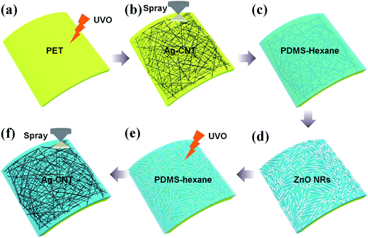
The experimental procedure of the piezoelectric bending motion sensor is described in Fig. 1. The bi-axially grown ZnO NRs were prepared by hydrothermal method17 and the experimental details were presented in ESI, S1.† The hybrid electrode of Ag NW–SWCNT was fabricated by spray-coating system. The Ag NWs solution [Nanopyxis, 1 wt% in distilled water] was diluted with deionized (DI) water to a concentration of 0.05 wt% through vigorous sonication and the SWCNT [Nano solution Co. Ltd., 1.3 wt% in distilled water stabilized by sodium dodecyl sulfonate (SDS) surfactants] was used as received without any purification. The Ag NW–SWCNT solution were prepared with several weight ratio of 9![[thin space (1/6-em)]](https://www.rsc.org/images/entities/char_2009.gif) :
:![[thin space (1/6-em)]](https://www.rsc.org/images/entities/char_2009.gif) 1, 8
1, 8![[thin space (1/6-em)]](https://www.rsc.org/images/entities/char_2009.gif) :
:![[thin space (1/6-em)]](https://www.rsc.org/images/entities/char_2009.gif) 2 and 7
2 and 7![[thin space (1/6-em)]](https://www.rsc.org/images/entities/char_2009.gif) :
:![[thin space (1/6-em)]](https://www.rsc.org/images/entities/char_2009.gif) 3 of 0.05 wt% Ag NW
3 of 0.05 wt% Ag NW![[thin space (1/6-em)]](https://www.rsc.org/images/entities/char_2009.gif) :
:![[thin space (1/6-em)]](https://www.rsc.org/images/entities/char_2009.gif) 1.3 wt% SWCNT to find out optimal composition value of hybrid electrode. Prior to the spray-coating, an ultraviolet ozone (UVO) treatment onto a polyethylene terephthalate (PET) film was conducted for 30 min to form hydrophilic surface as shown in Fig. 1a. The UVO treated PET film was then placed in bottom with distance 30 cm away from the spray nozzle and spray-coated with continuous feeding of the Ag NW–SWCNT sources through syringe pump and air flow (Fig. 1b). The spray-coating was conducted at an injection rate of 0.2 ml min−1 Ag NW–SWCNT with an air pressure of 2 bar for 2 min and the hot plate was set at 100 °C for evaporation of the water solvent. The spray-coated PET substrate was washed with DI water for a removal of the SDS surfactant from SWCNT solution. Then, the Ag NW–SWCNT spray-coated PET film was spin-coated with PDMS solution (PDMS
1.3 wt% SWCNT to find out optimal composition value of hybrid electrode. Prior to the spray-coating, an ultraviolet ozone (UVO) treatment onto a polyethylene terephthalate (PET) film was conducted for 30 min to form hydrophilic surface as shown in Fig. 1a. The UVO treated PET film was then placed in bottom with distance 30 cm away from the spray nozzle and spray-coated with continuous feeding of the Ag NW–SWCNT sources through syringe pump and air flow (Fig. 1b). The spray-coating was conducted at an injection rate of 0.2 ml min−1 Ag NW–SWCNT with an air pressure of 2 bar for 2 min and the hot plate was set at 100 °C for evaporation of the water solvent. The spray-coated PET substrate was washed with DI water for a removal of the SDS surfactant from SWCNT solution. Then, the Ag NW–SWCNT spray-coated PET film was spin-coated with PDMS solution (PDMS![[thin space (1/6-em)]](https://www.rsc.org/images/entities/char_2009.gif) :
:![[thin space (1/6-em)]](https://www.rsc.org/images/entities/char_2009.gif) hexane in 5
hexane in 5![[thin space (1/6-em)]](https://www.rsc.org/images/entities/char_2009.gif) :
:![[thin space (1/6-em)]](https://www.rsc.org/images/entities/char_2009.gif) 5 weight ratio) at 3000 rpm for 30 s and cured at 85 °C for 30 min, as shown in Fig. 1c. Using a paint brush, bi-axially grown ZnO NRs were randomly spread out onto PDMS layer through simple rubbing process until a monolayer of ZnO NRs was obtained (Fig. 1d). Another PDMS layer was then covered the monolayer of ZnO NRs, subsequently followed by the UVO treatment after the PDMS curing (Fig. 1e). Finally, the spray-coating of Ag NW–SWCNT was carried out for the formation of top electrode in the same weight ratio as the bottom electrode and Cu wires were connected to the both electrodes for electric measurement (Fig. 1f).
5 weight ratio) at 3000 rpm for 30 s and cured at 85 °C for 30 min, as shown in Fig. 1c. Using a paint brush, bi-axially grown ZnO NRs were randomly spread out onto PDMS layer through simple rubbing process until a monolayer of ZnO NRs was obtained (Fig. 1d). Another PDMS layer was then covered the monolayer of ZnO NRs, subsequently followed by the UVO treatment after the PDMS curing (Fig. 1e). Finally, the spray-coating of Ag NW–SWCNT was carried out for the formation of top electrode in the same weight ratio as the bottom electrode and Cu wires were connected to the both electrodes for electric measurement (Fig. 1f).
The crystallinity and morphology of ZnO NRs were investigated by an X-ray diffractometer (XRD) [Bruker New D8 Advance] and a field emission-scanning electron microscopy (FE-SEM) [Hitachi S-4800], respectively. Moreover, the morphology and electrical conductivity of Ag NW–SWCNT hybrid electrodes were observed by an optical microscope (OM) [Olympus U-CMAD3], a high resolution scanning transmission electron microscopy (HRSTEM) [JEM-2100F] and four-point probe resistivity measurement system [sourcemeter: Keithley 2400 and multimeter: Agilent 34410A]. Finally, the output voltages of the piezoelectric bending motion sensors were measured using an oscilloscope [Tektronix MDO3024].
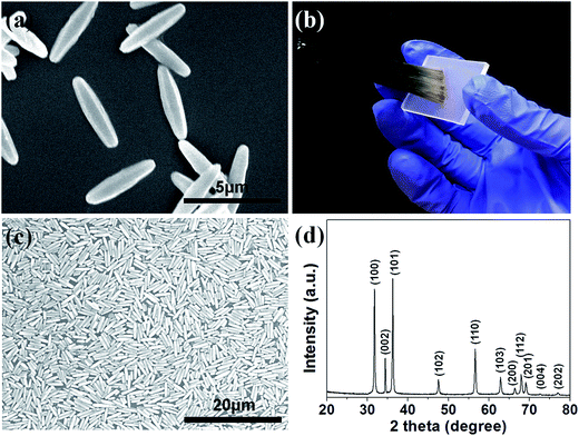
Fig. 2 shows the characteristics of the bi-axially grown ZnO NRs. The bi-axial ZnO NRs were uniformly grown from a hydrothermal synthesis as shown in FE-SEM image of Fig. 2a. The average diameter and length were 373.5 nm and 3.52 μm each. The hydrothermally grown ZnO NR powder was poured onto PDMS layer and rubbed using a soft paint brush to be spread out until a thin monolayer of ZnO NRs was completely filled out the bare PDMS layer as shown in Fig. 2b. The dense and continuous monolayer of bi-axially grown ZnO NRs was observed in FE-SEM image of Fig. 2c. Since the rubbing of ZnO NRs using a soft paint brush took only small forces, the ZnO NRs could be spread onto PDMS layer without any mechanical cracks. The main mechanism for the attachment of ZnO NRs onto PDMS is the van der Waals forces, which is the intermolecular forces between the molecules and surfaces.18 The rubbing direction of ZnO NRs onto the PDMS was random for identical output performance of piezoelectric bending motion sensor for any direction of bending. To characterize the crystalline phase of ZnO NRs, powder XRD was carried out as shown in Fig. 2d. The major XRD patterns were indexed in (100), (002), (101), (102), (110), (103), (201), indicating the wurtzite structure of crystalline ZnO.19 Thermal stability and decomposition temperature of ZnO NRs were also characterized by thermogravimetric analysis-differential scanning calorimetry (TGA-DSC) as shown in Fig. S2a.† Endothermic reaction with only 2.88% weight loss of ZnO NRs indicates the superior stability of as-synthesized ZnO NRs. Finally, to analyze the surface structure and compositional information, X-ray photoelectron spectrometry (XPS) was conducted as shown in Fig. S3.†
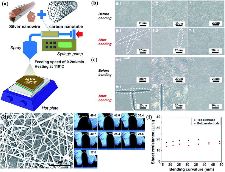
The spray-coating of Ag NW–SWCNT was attempted with several experimental conditions to find out optimal component value of hybridized Ag NWs and SWCNT. 9, 8, and 7 g of 0.05 wt% Ag NWs in DI water and 1, 2, and 3 g of 1.3 wt% SWCNT also in DI water were mixed respectively via vigorous sonication and prepared for spray-coating. With customized spray coating setup as shown in Fig. 3a, the Ag NW–SWCNT composite film was spray-coated without agglomeration. The spray-coated hybridized Ag NW–SWCNT electrodes were tested before and after 10 times mechanical bending through OM observation. As shown in Fig. 3b and c, the mechanical cracks were observed after the bending of electrodes in both case of bottom and top electrodes in weight ratio of 9![[thin space (1/6-em)]](https://www.rsc.org/images/entities/char_2009.gif) :
:![[thin space (1/6-em)]](https://www.rsc.org/images/entities/char_2009.gif) 1 and 8
1 and 8![[thin space (1/6-em)]](https://www.rsc.org/images/entities/char_2009.gif) :
:![[thin space (1/6-em)]](https://www.rsc.org/images/entities/char_2009.gif) 2 (g/g) of 0.05 wt% Ag NW
2 (g/g) of 0.05 wt% Ag NW![[thin space (1/6-em)]](https://www.rsc.org/images/entities/char_2009.gif) :
:![[thin space (1/6-em)]](https://www.rsc.org/images/entities/char_2009.gif) 1.3 wt% SWCNT. This is because of the unstable inter-connection between Ag NWs and also the poor adhesion of Ag NWs onto the PET due to the lack of SWCNT content.20 Otherwise, the continuous morphology of Ag NW–SWCNT was observed in case of 7
1.3 wt% SWCNT. This is because of the unstable inter-connection between Ag NWs and also the poor adhesion of Ag NWs onto the PET due to the lack of SWCNT content.20 Otherwise, the continuous morphology of Ag NW–SWCNT was observed in case of 7![[thin space (1/6-em)]](https://www.rsc.org/images/entities/char_2009.gif) :
:![[thin space (1/6-em)]](https://www.rsc.org/images/entities/char_2009.gif) 3 (g/g), indicating the effect of SWCNT content in the hybridized electrode. Accordingly, this indicates that the SWCNT functioned as an inter-connector between the Ag NWs for continuous morphology. Moreover, the SWCNT functioned also as an adhesion agent for better cohesion of Ag NWs to the PET substrate. The spray-coated Ag NW–SWCNT hybrid electrode onto PET substrate with optimal component ratio of 7
3 (g/g), indicating the effect of SWCNT content in the hybridized electrode. Accordingly, this indicates that the SWCNT functioned as an inter-connector between the Ag NWs for continuous morphology. Moreover, the SWCNT functioned also as an adhesion agent for better cohesion of Ag NWs to the PET substrate. The spray-coated Ag NW–SWCNT hybrid electrode onto PET substrate with optimal component ratio of 7![[thin space (1/6-em)]](https://www.rsc.org/images/entities/char_2009.gif) :
:![[thin space (1/6-em)]](https://www.rsc.org/images/entities/char_2009.gif) 3 (0.05 wt% Ag NW
3 (0.05 wt% Ag NW![[thin space (1/6-em)]](https://www.rsc.org/images/entities/char_2009.gif) :
:![[thin space (1/6-em)]](https://www.rsc.org/images/entities/char_2009.gif) 1.3 wt% SWCNT) was observed through FE-SEM as shown in Fig. 3d. The Ag NW–SWCNT composite film was uniformly coated without agglomeration. The Ag NW–SWCNT electrode was also observed by HRSTEM for better observation (Fig. S4†). The Ag NWs were dark color column and the ash-colored SWCNT was entangled in gap of the Ag NWs, filling up the vacant room between the Ag NWs and making an inter-connection of Ag NWs. Fig. S4b† shows the central region image of Ag NW–SWCNT, indicating the crystalline lattice of Ag NWs and electron diffraction pattern of individual Ag NWs in Fig. S4c† revealed the pentagonal rotational periodicity.
1.3 wt% SWCNT) was observed through FE-SEM as shown in Fig. 3d. The Ag NW–SWCNT composite film was uniformly coated without agglomeration. The Ag NW–SWCNT electrode was also observed by HRSTEM for better observation (Fig. S4†). The Ag NWs were dark color column and the ash-colored SWCNT was entangled in gap of the Ag NWs, filling up the vacant room between the Ag NWs and making an inter-connection of Ag NWs. Fig. S4b† shows the central region image of Ag NW–SWCNT, indicating the crystalline lattice of Ag NWs and electron diffraction pattern of individual Ag NWs in Fig. S4c† revealed the pentagonal rotational periodicity.
The examination of sheet resistance in Fig. 3f was conducted to measure the electrical conductivity of Ag NW–SWCNT electrodes at an optimized weight ratio (7![[thin space (1/6-em)]](https://www.rsc.org/images/entities/char_2009.gif) :
:![[thin space (1/6-em)]](https://www.rsc.org/images/entities/char_2009.gif) 3 of 0.05 wt% Ag NW
3 of 0.05 wt% Ag NW![[thin space (1/6-em)]](https://www.rsc.org/images/entities/char_2009.gif) :
:![[thin space (1/6-em)]](https://www.rsc.org/images/entities/char_2009.gif) 1.3 wt% SWCNT) according to the different bending curvature (Fig. 3e). The sheet resistance for the non-bent bottom and top electrodes of Ag NW–SWCNT was 15.86 and 14.50 Ω □−1, respectively. Otherwise, it is notable that the value of sheet resistance is considerably consistent according to the applied bending curvature with average values of 15.13 and 18.14 Ω □−1 for both bottom and top electrodes. This mechanically stable and robust hybridized Ag NW–SWCNT is adequate as an electrode for practical bending motion sensor system.
1.3 wt% SWCNT) according to the different bending curvature (Fig. 3e). The sheet resistance for the non-bent bottom and top electrodes of Ag NW–SWCNT was 15.86 and 14.50 Ω □−1, respectively. Otherwise, it is notable that the value of sheet resistance is considerably consistent according to the applied bending curvature with average values of 15.13 and 18.14 Ω □−1 for both bottom and top electrodes. This mechanically stable and robust hybridized Ag NW–SWCNT is adequate as an electrode for practical bending motion sensor system.
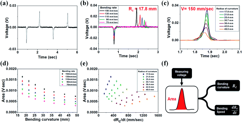
The standard output voltage signals were measured as shown in Fig. 4a. The measurement condition for the standard output was set in bending curvature of 17.8 mm and speed of 150 mm s−1. As previous shown in Fig. 3e, conditions for the bending curvature is separated as 49.0, 42.6, 36.4, 30.7, 25.4, 21.6 and 17.8 mm. The bending speed was also divided into five values with reduction of 20 mm s−1 from the maximum value of 150 mm s−1, 150, 130, 110, 90 and 70 mm s−1 each. However, performance of the piezoelectric bending motion sensor under bending speed lower than 70 mm s−1 had difficulty in classification of the output signals because too slow bending operation vanished the part of piezoelectric potential generation. Fig. 4b and c show the output performance of piezoelectric bending motion sensor according to different bending speed and curvature at constant bending curvature and speed. At constant bending curvature of 17.8 mm, the output voltages were measured according to the bending speed as shown in Fig. 4b. From the graph, it is notable that the bending speed is a factor deciding the peak voltages of output power. At constant bending speed of 150 mm s−1, the peak voltage was increased with decreasing bending curvature (more bending incurvation in smaller value of bending curvature). However, the area of output voltages was also increased with decreasing bending curvature. This indicates that the voltage area is a factor depending on the value of bending curvature. Accordingly, the applied bending curvature across the piezoelectric bending motion sensor affects both the voltage peak and area and therefore, the output performance is needed to be considered in aspects of voltage area not only in voltage peak. Accordingly, if the voltage area according to the bending curvature and speed is presented respectively, the correlation between these factors will be enabled to be ratiocinated. Therefore, the voltage area was calculated and presented as a function of applied bending curvature and speed. The values of voltage area were positively transformed in case of negative output voltage peaks. In this report, concave bending was applied to the piezoelectric bending motion sensor and therefore negative output voltages were initially measured during the bending motion, otherwise positive values were reversely examined during release motion. Since only bending motions was considered in whole bending and release motions for the applicability of both bending and release modes, the values of voltage area for bending motion were all transformed to positive one in case of the concave bending. The voltage area values for release mode were also shown in Fig. S5.†
The values of voltage area as a function of bending curvature and rate (dRc/dt) were presented in Fig. 4d and e. The measurement was attempted with five different bending motion sensors at the same experimental conditions in each case for accuracy. In addition, to secure the reliability of piezoelectric bending motion sensor, measurement of the output performance was conducted for every 1000 times during 4000 times bending motions of the piezoelectric sensor to insure the constant power generation (Fig. S6†). Finally, to verify that the electrical outputs were generated by piezoelectric properties of ZnO NRs, non-ZnO NRs contained PDMS and Ag NW–SWCNT bending device was taken into an experiment (Fig. S7†). The output voltage shown by the non-ZnO NR bending device (Fig. S7b†) was only noise level, indicating that the output signals came from the piezoelectric effect of the ZnO NRs. The relative bending rate for bending of piezoelectric motion sensor can be calculated as
 | (1) |
 | (2) |
 | (3) |
Accordingly, the integration value of piezoelectric charge over capacitance indicates the average charge generated by the external bending motion of the piezoelectric sensor over capacitance. Therefore, since the capacitance value is consistent, the generated charge is proportional to the voltage area value. Generally, an area of voltage signals is consistent with piezoelectric charges and charges are dependent on bending curvature. In other words, under the same applied bending curvature, the peak area values should be the same. However, discrepancy in voltage area value at the same bending curvature under different bending speed was observed. This discordance in piezoelectric charge values is attributed to resistor–capacitor (RC) time constant, which allows charge leakage during bending operations in case of different bending speed conditions. Since more leakages in piezoelectric charges occurred in mode of slower bending speed of the piezoelectric units, the resultant piezoelectric charges, which can be substituted to the area values were smaller. This theory is fundamentally based on a piezoelectric effect,
![[q with combining dot above]](https://www.rsc.org/images/entities/i_char_0071_0307.gif) = d33EAε = d33EAε
| (4) |
![[q with combining dot above]](https://www.rsc.org/images/entities/i_char_0071_0307.gif) is the piezoelectric charge divided by period of time, d33 is the piezoelectric charge constant, ε is the bending speed, and E, A are the Young's modulus and the applied area each.21 Therefore, the absolute area values of output voltages also change with applied bending speed across the piezoelectric bending motion sensor. Due to this reason, the piezoelectric output performance is needed to be analyzed in consideration of bending speed as well as the bending curvature for accurate sensing system. Based on this theory, our group actually tested the piezoelectric bending motion sensor via simultaneous observation of bending curvature and speed and verified that the database of the voltage area values was somewhat consistent according bending curvature and speed.
is the piezoelectric charge divided by period of time, d33 is the piezoelectric charge constant, ε is the bending speed, and E, A are the Young's modulus and the applied area each.21 Therefore, the absolute area values of output voltages also change with applied bending speed across the piezoelectric bending motion sensor. Due to this reason, the piezoelectric output performance is needed to be analyzed in consideration of bending speed as well as the bending curvature for accurate sensing system. Based on this theory, our group actually tested the piezoelectric bending motion sensor via simultaneous observation of bending curvature and speed and verified that the database of the voltage area values was somewhat consistent according bending curvature and speed.
The strategy for detection of bending motions is shown in Fig. 4f. Firstly, measurement of output voltages across the piezoelectric bending motion sensor is needed to be conducted. Secondly, calculation of voltage area is required and the area values are needed to be indicated in graphs, which display x versus y values as bending curvature or bending rate versus voltage area. Finally, collation of the original database from the statistical measurement of output performance with experimental data is needed to be conducted to find out the values of bending curvature and speed.
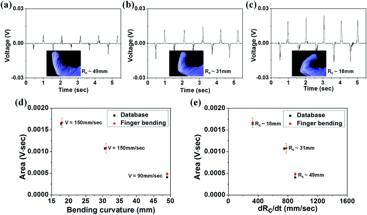
Practically, the piezoelectric bending motion sensors experienced finger bending with random bending curvatures and speeds among the experimental conditions set-up. The output voltages were measured using an oscilloscope as can be seen in Fig. 5a–c. From the calculation of voltage area based on values of output voltage across the piezoelectric bending motion sensor, the experimental data of voltage area was presented. The information of bending rate from the graph of bending curvature versus voltage area, and bending curvature from the graph of bending rate versus voltage area was able to be obtained. For example, the voltage area value, 0.001665 V s was obtained and the 0.00167 V s for bending curvature of 17.8 mm and bending speed 150 mm s−1 from the database of the output performance was almost the same. Therefore, from the voltage area value, the bending curvature and speed for Fig. 5a could be speculated, which were 17.8 mm and 150 mm s−1. However, due to the small scale of the database, the random bending curvature and speed were restricted to several values only. Accordingly, diverse range of bending curvature and speed values from experimental set-up is required for the future study. Continuously, the another point of voltage area value was 0.001078 V s which coincided with voltage area value of 0.00107 V s for bending curvature of 30.7 mm and bending speed of 150 mm s−1 from the database as shown in Fig. 5d and e. Finally, bending curvature and speed of 49 mm and 90 mm s−1 for voltage area value of 0.000485 V s from the database and experimental value of 0.000478 V s were found to be almost identical. As a result, the bending curvature and speed for Fig. 5b and c were 30.7 mm & 150 mm s−1 and 17.8 mm & 90 mm s−1. Actually, the applied bending curvatures were measured from the photographs of piezoelectric sensors during bending operation and the values were about 49, 31 and 18 mm each. Hence, the applied bending curvatures were good accordance with the speculated bending curvatures. Therefore, under specific conditions of bending curvatures and speeds of the piezoelectric sensor, the bending motions are predictable from the simple correlation of voltage area and bending curvature and speed. Beyond presenting the output results according only by different bending curvatures, this result discerned the bending curvature and speed in simultaneous manner for perspicacious analysis, which was based on the theory of piezoelectric effect.
In conclusion, highly bendable and wearable piezoelectric motion sensor was successfully demonstrated by detection of bending motions as a function of bending curvature and speed. Based on the theory of a piezoelectric effect, the correlation of voltage area value with bending curvature and speed was discovered and enabled the speculation of bending curvature and speed under specific experimental bending conditions. Moreover, high elasticity of the piezoelectric bending motion sensor is attributed to the flexible elements of piezoelectric composite material of ZnO NR–PDMS and hybrid Ag NW–SWCNT electrodes. This piezoelectric bending motion sensor is applicable to the human artificial skin as well as biomimetic robot system.
Acknowledgements
This research was supported by the Next-generation Medical Device Development Program for Newly-Created Market (No. 2015M3D5A106 5907) and R&D Result Diffusion Program (No. NRF-2015R1A2A1A15053165) of the National Research Foundation (NRF) of Korea funded by the Korean government (MSIP).Notes and references
- D.-H. Kim, N. Lu, R. Ma, Y.-S. Kim, R.-H. Kim, S. Wang, J. Wu, S. M. Won, H. Tao, A. Islam, K. J. Yu, T. Kim, R. Chowdhury, M. Ying, L. Xu, M. Li, H.-J. Chung, H. Keum, M. McCormick, P. Liu, Y.-W. Zhang, F. G. Omenetto, Y. Huang, T. Coleman and J. A. Rogers, Science, 2011, 333, 838 CrossRef CAS PubMed.
- Y. Khan, A. E. Ostfeld, C. M. Lochner, A. Pierre and A. C. Arias, Adv. Mater., 2016, 28, 4373 CrossRef CAS PubMed.
- G. Schwartz, B. C. K. Tee, J. Mei, A. L. Appleton, D. H. Kim, H. Wang and Z. Bao, Nat. Commun., 2013, 4, 1859 CrossRef PubMed.
- F. Ilievski, A. D. Mazzeo, R. F. Shepherd, X. Chen and G. M. Whitesides, Angew. Chem., Int. Ed., 2011, 50, 1890 CrossRef CAS PubMed.
- T. Yamada, Y. Hayamizu, Y. Yamamoto, Y. Yomogida, A. I. Najafabadi, D. N. Futaba and K. Hata, Nat. Nanotechnol., 2011, 6, 296 CrossRef CAS PubMed.
- C. Pang, G.-Y. Lee, T. Kim, S. M. Kim, H. N. Kim, S.-H. Ahn and K.-Y. Suh, Nat. Mater., 2012, 11, 795 CrossRef CAS PubMed.
- J. Park, Y. Lee, J. Hong, Y. Lee, M. Ha, Y. Jung, H. Lim, S. Y. Kim and H. Ko, ACS Nano, 2014, 8, 12020 CrossRef CAS PubMed.
- S. Gong, D. T. H. Lai, B. Su, K. J. Si, Z. Ma, L. W. Yap, P. Guo and W. Cheng, Adv. Electron. Mater., 2015, 1, 1400063 CrossRef.
- Y. Cheng, R. Wang, J. Sun and L. Gao, Adv. Mater., 2015, 27, 7365 CrossRef CAS PubMed.
- M. H. G. Wichmann, S. T. Buschhorn, L. Böger, R. Adelung and K. Schulte, Nanotechnology, 2008, 19, 475503 CrossRef PubMed.
- L. Cai, L. Song, P. Luan, Q. Zhang, N. Zhang, Q. Gao, D. Zhao, X. Zhang, M. Tu, F. Yang, W. Zhou, Q. Fan, J. Luo, W. Zhou, P. M. Ajayan and S. Xie, Sci. Rep., 2013, 3, 3048 Search PubMed.
- J.-S. Heo, J.-H. Chung and J.-J. Lee, Sens. Actuators, A, 2006, 126, 312 CrossRef CAS.
- M. Ramuz, B. C.-K. Tee, J. B.-H. Tok and Z. Bao, Adv. Mater., 2012, 24, 3223 CrossRef CAS PubMed.
- J. Chun, N.-R. Kang, J. -Y. Kim, M.-S. Noh, C.-Y. Kang, D. Choi, S.-W. Kim, Z. L. Wang and J. M. Baik, Nano Energy, 2015, 11, 1 CrossRef CAS.
- E. S. Nour, C. O. Chey, M. Willander and O. Nur, Nanotechnology, 2015, 26, 095502 CrossRef CAS PubMed.
- C. Chang, V. H. Tran, J. Wang, Y.-K. Fuh and L. Lin, Nano Lett., 2010, 10, 726 CrossRef CAS PubMed.
- W. S. Jang, T. I. Lee, J. Y. Oh, S. H. Hwang, S. W. Shon, D. H. Kim, Y. Xia, J. M. Myoung and H. K. Baik, J. Mater. Chem., 2012, 22, 20719 RSC.
- T. I. Lee, W. S. Jang, E. Lee, Y. S. Kim, Z. L. Wang, H. K. Baik and J. M. Myoung, Energy Environ. Sci., 2014, 7, 3994 Search PubMed.
- X. Hou, L. Wang, G. He and J. Hao, CrystEngComm, 2012, 14, 5158 RSC.
- J. Lee, J. Y. Woo, J. T. Kim, B. Y. Lee and C.-S. Han, ACS Appl. Mater. Interfaces, 2014, 6, 10974 CAS.
- J. Sirohi and I. Chopra, J. Intell. Mater. Syst. Struct., 2000, 11, 246 CrossRef CAS.
Footnote |
| † Electronic supplementary information (ESI) available. See DOI: 10.1039/c6ra25797f |
| This journal is © The Royal Society of Chemistry 2017 |

