Interface-engineered charge separation at selective electron tunneling heterointerfaces†
Chunhui
Gu‡
 a,
Chuancheng
Jia‡
 a and
Xuefeng
Guo
 *ab
*ab
aBeijing National Laboratory for Molecular Sciences, State Key Laboratory for Structural Chemistry of Unstable and Stable Species, College of Chemistry and Molecular Engineering, Peking University, Beijing 100871, P. R. China. E-mail: guoxf@pku.edu.cn
bDepartment of Materials Science and Engineering, College of Engineering, Peking University, Beijing 100871, P. R. China
First published on 27th July 2017
Abstract
The phenomena of charge/energy transfer commonly exist at most heterointerfaces. These processes vary with the change of the electronic structure at the interface, which leads to the diversity of device functionalities. Therefore, interface engineering is a powerful approach to control the charge/energy transfer behavior by modulating the interfacial electronic structure. On the basis of a novel ipsilateral selective electron tunneling (ISET) mechanism, we systematically investigated the charge transfer property at a semiconductor/graphene/photoactive material ternary interface. With acridine orange dye as the photoactive material, photoinduced electrons from the dye can directly tunnel across the TiO2/graphene Schottky barrier into the conductive band of TiO2, while the photoinduced holes were collected by graphene. These results demonstrate the capability of such an ISET-based ternary interface to achieve efficient charge transfer and separation, promising the fabrication of new types of photovoltaic and optoelectronic devices.
Introduction
The control of charge/energy transfer occurring at heterointerfaces is crucial to produce high-performance functional electronic devices, such as field effect transistors (FETs),1 photovoltaics2 and molecular electronic devices.3 In general, the electronic structure at the heterointerface, which is determined by the properties of the materials used, plays the key role in controlling the charge/energy transfer process. For instance, Schottky barriers exist at some semiconductor/metal interfaces and p–n junctions exist between semiconductors with different doping. These heterointerfaces have specific properties such as rectification and charge separation, which are important to build logical circuits, photodetectors, solar cells and so on. In addition, the interfacial properties between the materials and their environment, especially two-dimensional materials with atomic thickness, are sensitive to external stimuli, showing great potential in the fabrication of ultrasensitive sensors.4 Therefore, effective heterointerface design and control are essential to realize functional devices with optimized performances.Low-dimensional carbon materials, including carbon nanotubes and graphene (Gr), have been extensively studied and widely applied in optoelectronic devices.4a,5 Due to the quantum size effect and their special electronic structure, these low-dimensional carbon materials usually show distinctive properties. For instance, graphene, as a classical low-dimensional carbon material with a single layer of hexagonally arranged sp2-bonded carbon atoms,6 shows excellent properties in electronics,7 mechanics and optics.8 In addition, because of its large surface area, graphene is easily modulated and ultrasensitive to the environment. Therefore, graphene with functionalized surfaces can be applied as a sensor with high selectivity and low detection limit.4,9 Due to the abnormal linear dispersion relationship near the Fermi level and the high transparency to phonons and electrons,8,10 the interfaces between graphene and semiconductors show distinctive charge/energy transfer behaviors, which imply great potential in the fabrication of novel functional devices.
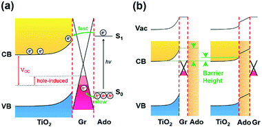
Recently we reported an ipsilateral selective electron tunneling (ISET) mechanism based on a unique semiconductor/Gr/dye ternary interface (Fig. 1a).11 In particular, a Schottky barrier is formed at the TiO2/Gr interface. Photoinduced electron–hole pairs produced from an acridine orange (Ado, as a photoactive material) layer diffuse along the same direction to graphene. The photoinduced electrons can inject into the TiO2 transport layer by crossing the Schottky barrier. In contrast, the photoinduced holes are collected by graphene, thus realizing effective charge separation at the TiO2/Gr/Ado ternary interface. In addition, both theoretical and experimental results showed that the electron injection speed is much faster than recombination. This yielded an ∼86.8% carrier collection efficiency. On the basis of these results, the behavior of charge transfer is directly related to the electronic structure of the heterointerface, which is significantly dependent on light illumination, material thickness and stacking sequence. To explore the rich charge-transfer behavior at such an ISET-based TiO2/Gr/Ado ternary interface, in this work we systemically studied the electronic structure of the ternary interface with different stacking sequences and thicknesses of the Ado layer, which is crucial to improve the fundamental understanding of how the ISET mechanism works.
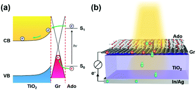 | ||
| Fig. 1 (a) Schematic of how the ipsilateral selective electron tunneling (ISET) mechanism works. (b) Structural representation of a photovoltaic device with a TiO2/Gr/Ado ternary interface. | ||
Results and discussion
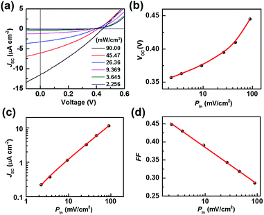
To do this, a series of TiO2/Gr/Ado ternary interfaces were obtained to produce the corresponding devices. The device structure is shown in Fig. 1b. Detailed fabrication processes are provided in the Experimental section. In brief, single-layer graphene was grown using a chemical vapor deposition (CVD) method on copper foils. Ado molecules were thermally evaporated on graphene and then annealed at 140 °C to ensure a homogeneous Gr/Ado interface. The thickness of the Ado layer was designed from 1 nm to 12 nm, which was carefully controlled by thermal evaporation and confirmed by AFM characterization (Fig. S1, ESI†). 100 nm In and 100 nm Ag were evaporated as Ohmic contact back electrodes on the rutile TiO2 (100) single crystals. The front surfaces of TiO2, which are atomically flat, were flushed using hydrofluoric acid and etched using oxygen plasma to reduce surface contaminants, which guarantees a compact TiO2–graphene interface. The Gr/Ado layers were transferred to TiO2 with the aid of PMMA to fabricate the corresponding TiO2/Gr/Ado ternary interfaces.Illumination intensity-dependent charge transfer behaviors of the TiO2/Gr/Ado ternary interface were firstly investigated. Fig. 2a shows the current–voltage (J–V) characteristics of a representative device (∼2 nm Ado thickness) measured under visible light illumination (>420 nm). Fig. 2b–d are derived from Fig. 2a, illustrating how the illumination intensity affects the open circuit voltage (VOC), the short circuit current (JSC) and the fill factor (FF), respectively. JSC is directly proportional to the illumination intensity, which is due to the fact that the number of excited Ado molecules is proportional to the intensity of incident photons. VOC, which changes from 0.357 V to 0.445 V with increasing illumination intensity, is nearly proportional to the logarithm of the illumination intensity. This is similar to the behavior of p–n junction-based photovoltaic devices that obey the Shockley eqn (E1),12 where n is a constant, k is the Boltzmann constant, t is the temperature, q is the electron's charge, JL is the photo-generated current, and J0 is the reverse saturation current.
 | (E1) |
However, considering the novel ISET mechanism at the TiO2/Gr/Ado ternary interface, a small shift of VOC to higher values indicates a better photovoltaic effect at high light intensities for the TiO2/Gr/Ado system. The results demonstrate that the trans-interface potential is determined by both the intrinsic electronic structure and non-equilibrium carrier caused by illumination excitation.
FF is equal to the maximum output power divided by VOC and JSC, representing how “square” the J–V curve is. The FF value evaluates the proportion of effective photocarrier separation during the photoinduced charge transfer at the heterointerface. Fig. 2d shows that FF decreases from 0.449 to 0.286 as the illumination intensity increases, indicating the increased photocarrier recombination at the TiO2/Gr/Ado ternary interface.13 Such an increased carrier recombination mainly comes from the rate-limiting effect of the charge-separated process at the Schottky barrier, which is identical to the behavior of traditional photovoltaic devices.
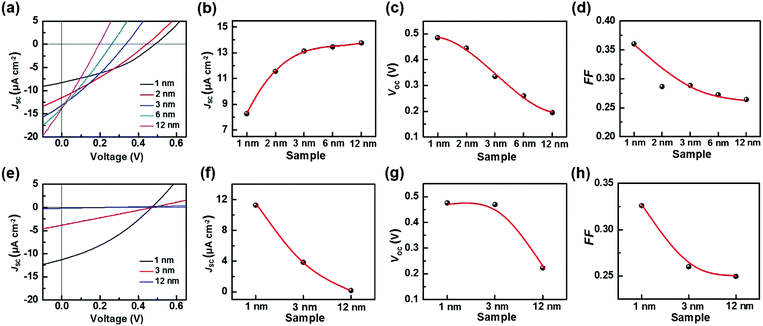
Besides the illumination intensity, the material thickness is crucial to the charge/energy transfer behavior at the heterointerfaces. For instance, the electron injection at the interface of molecular electronic devices depends on the thickness of the molecular layer.14 Furthermore, in organic solar cells, the thickness-dependent charge/energy transfer behavior at the interfaces of electron/hole transporting materials also exists, which significantly affects the aggregation behavior, and the charge recombination and electron scattering process at the interfaces.15 Therefore, in the current work, the Ado thickness-dependent charge transfer behavior of the TiO2/Gr/Ado ternary interface was investigated. Fig. 3a shows the current–voltage characteristics of the devices with different Ado thicknesses under visible light illumination of 90 mW cm−2. Upon increasing the Ado thickness from 1 to 12 nm, it is intriguing to find that JSC increases from 8.28 to 12.77 μA cm−2 (Fig. 3b), which is obviously attributed to the increased absorption of the Ado layer. We noticed an intense convex shape in the relationship between Ado thickness and JSC, and the device with ∼1 nm Ado achieved nearly ∼60% JSC compared to the one with ∼12 nm Ado. Such results indicate that additional Ado molecules make a minor contribution to the JSC in comparison with superficial ones, due to the limitation of the exciton diffusion free path. VOC decreases from 0.485 V to 0.195 V with increasing illumination (Fig. 3c). On the other hand, in the dark the J–V properties of all these heterointerfaces were uniform (Fig. S19a, ESI†), indicating that the Schottky barriers at the TiO2/Gr interfaces are not obviously affected by the accumulation of Ado molecules. Therefore, it is reasonable to believe that such an Ado thickness-dependent VOC is related to the non-equilibrium process induced by photoirradiation.
To investigate the non-equilibrium process at the TiO2/Gr/Ado ternary interface, we applied transient photoluminescence (PL) to study the dynamics of photo-induced charge separation, collection and combination. For the samples with 1 nm or 12 nm Ado layers, the PL decay traces could be fitted according to a triple exponential decay function (Fig. S21, ESI†). The decay times for both traces were fitted to τ1 = ∼2 ns, τ2 = ∼8 ns and τ3 = ∼62 ns, corresponding to the mean times of photoinduced electron injection into TiO2 (τ1), graphene (τ2) and the intrinsic interband recombination of Ado excitons (τ3), where the last two processes are ineffective recombination processes.11 Although the two samples have similar PL decay times, the contribution proportion of the three processes were different from each other. Along with the Ado thickness increase from 1 nm to 12 nm, the contribution proportion of τ1 decreased from 55.2% to 23.8% while τ3 increased from 13.3% to 41.3%. The increased recombination is attributed to the long distance for excitons diffusing through a thick Ado layer to the ternary interface for effective separation. The charge recombination process during such a long-distance diffusion also causes the decrease of the fill factor (Fig. 3d) and VOC to some extent.
In addition, the transient photovoltage methods were applied to measure the rise time of the transient voltage at the TiO2/Gr/Ado interface. The time-dependent photovoltage traces (Fig. S22, ESI†) can be fitted to a double exponential function with two rise times. The faster rise time corresponds to the process of photoinduced electron injection, transportation through TiO2 and final collection by the In/Ag back contact electrode. The slower rise time corresponds to the process of photoinduced hole collection by the graphene layer. The fitted faster/slower rise times were 111.7 μs/602.2 μs for the sample with 1 nm Ado and 121.4 μs/1340.9 μs for the sample with 12 nm Ado, respectively. These results show that the process of hole collection is much slower than that of electron collection (∼2 ns), especially for thick Ado layers. Therefore, the photoinduced holes are easily accumulated in the Ado layer, which can induce opposite negative charges in the graphene layer, similar to the gating effect in the FET devices.4b,16 Such a hole-induced gating effect can effectively enhance the Fermi level of graphene, thus causing the decrease of VOC (Fig. 4a).
For further understanding the ISET effect at the TiO2/Gr/Ado interface, we fabricated a traditional TiO2/Ado/Gr interface as a control. Fig. 3e shows the J–V characteristics of the TiO2/Ado/Gr ternary interface with Ado thicknesses from 1 nm to 12 nm under the illumination of 90 mW cm−2. We found that JSC and VOC decayed rapidly along with the increase of Ado thicknesses (Fig. 3f and g). Especially, the J–V characteristics became linear along with the increase of Ado thicknesses, which led to the FF decrease from 0.326 to 0.250 (Fig. 3h) at a faster decay rate than that containing the TiO2/Gr/Ado interface (from 0.361 to 0.264, Fig. 3d), indicating the increase of charge recombination. For charge separation in photovoltaic devices with different heterointerfaces, the formation of the depletion layer is of crucial importance. In the case of the TiO2/Gr/Ado ternary interface in the dark, the J–V characteristics show that the rectifying behaviors scarcely vary with increasing Ado thickness (Fig. S19a, ESI†), indicating a stable and robust Schottky barrier at the TiO2/Gr interface. In contrast, although the depletion layer is able to form at the TiO2/Ado/Gr ternary interface, the rectifying characteristics rapidly decay with increasing Ado thickness (Fig. S19b, ESI†), indicating the reduced Schottky barrier height (Fig. 4b). The breakdown of the depletion layer is evidently unfavorable for charge separation, thus damaging photoelectric conversion in TiO2/Ado/Gr devices. In addition, the series resistance of photosensitive agents is another problem existing at the TiO2/Ado/Gr ternary interface, while the TiO2/Gr/Ado structure partly avoids this problem. As it is more difficult for charges to diffuse through thick Ado layers in the TiO2/Ado/Gr device, more electron/hole pairs recombine during the diffusion process. Therefore, owing to the robust depletion layer and without the problem of the series resistance of photosensitive agents for the TiO2/Gr/Ado ternary interface, the ISET-based heterointerfaces have obvious advantages for efficient charge separation.
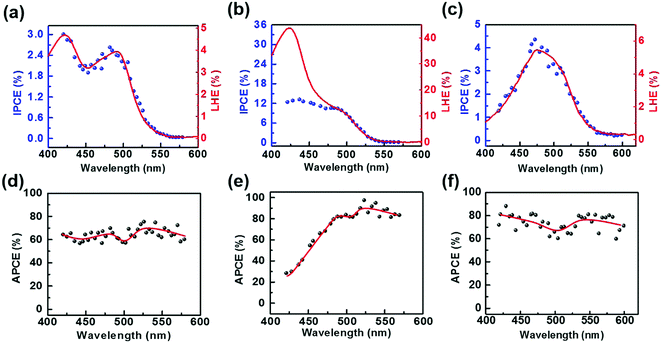
To further investigate the charge-separation behavior of the TiO2/Gr/Ado ternary interface, the photon-to-current conversion efficiency (IPCE) of the devices, which is equal to the ratio between separated electrons/holes and photon intensity, is measured as a function of wavelength. Fig. 5a shows the IPCE spectrum (blue dot) of a TiO2/Gr/Ado device with ∼1 nm Ado, which is quite like the light harvesting efficiency (LHE) spectrum (red line) of the corresponding Ado film dispersed on Gr. As a comparison, the IPCE spectrum for a device with a 12 nm Ado layer does not conform to the corresponding LHE spectrum (Fig. 5b), especially in the range of λ < 480 nm. To further evaluate the charge separation efficiency of the interface, we calculated the absorbed photon-to-current efficiency (APCE), which is equal to the IPCE divided by the LHE, reflecting the intrinsic quantum efficiency of photoinduced charge separation. The APCE is uniform in the range of 420 nm to 550 nm for a ∼1 nm Ado device (Fig. 5d), while the APCE decays rapidly when the wavelength is below 480 nm for a ∼12 nm Ado device (Fig. 5e).
To understand such a difference, the intrinsic optical properties of the Ado layer were studied. The solid-state UV-Vis spectrum shows the maximum absorption of the Ado dye on Gr at 421 nm and 492 nm (Fig. S3, ESI†), which is consistent with the IPCE spectrum. Along with the increase of the Ado thickness, the absorption at 421 nm increases more rapidly than that at 492 nm. This result hints that the absorption at the wavelength of 421 nm is related to molecular aggregation, which conforms to the concentration gradient experiments in solution (Fig. S3f, ESI†). To some extent, the aggregation of photosensitive agents, which commonly exists in fluorescence devices,17 organic electronics18 and solar cells,19 leads to the decay of APCE. In comparison with single-molecule absorption, which mainly possesses electron excitation from S0 to S1 states, aggregation-involved absorption is more complicated. Besides electron excitation, inter-molecular processes, such as inter-molecular electron transfer and the formation of electroplexes, contribute considerably to the absorption. However, such processes do not contribute to any photoinduced excitons. In addition to molecular aggregation, the slow hole injection rate is another considerable reason for the APCE decay. Now that the hole injection proves to be the rate-limiting step of the photovoltaic process (Fig. S22, ESI†), where the rate for hole injection with the time scale of a few hundred μs is much slower than the rate of electron injection with the time scale of a few ns (Fig. S21, ESI†), the increased excitons could not be effectively separated at the heterointerfaces. Therefore, the photocurrent reaches saturation due to the hole injection limit, which causes the decrease of the apparent APCE values. Furthermore, it is worthy noting that the unseparated excitons will be quenched via an interband recombination process and cause the decay of FF, which is in agreement with the experiment.
The IPCE spectrum of the TiO2/Ado/Gr interface was also measured as a control (Fig. 5c). The IPCE spectrum shows a broadened peak with the maximum at 472 nm, which conforms to the corresponding LHE spectrum. Such a LHE spectrum varies a lot, in comparison with the TiO2/Gr/Ado structure and free molecules in solution. The calculated APCE spectrum of the TiO2/Ado/Gr interface with ∼1 nm Ado (Fig. 5f) shows slightly larger APCE values than those of the TiO2/Gr/Ado system (Fig. 5d). The AFM image (Fig. S2, ESI†) shows that severe aggregation occurs on the TiO2 surface, while a uniform flat layer is formed on the surface of Gr coated TiO2. The aggregation behavior of Ado molecules, which is controlled by the properties of the surface, significantly affects the absorption spectrum. Due to the hydrophilic surface of TiO2, Ado molecules aggregate on TiO2, which causes a bad contact at the Ado/TiO2 interface. In contrast, Ado molecules stack and interact with the hydrophobic graphene surface through π–π interaction. The absorption of the Ado/Gr layer almost conforms to the free molecules in solvent, indicating that Ado molecules disperse well on graphene and even keep the properties of single-molecule states for a thin Ado layer. Such an interfacial structure determines a strengthened Ado molecule–graphene interaction, which is favorable to the charge transfer and separation process.
Conclusion
In conclusion, we systematically studied the charge/energy transfer behaviors of the ISET-based TiO2/Gr/Ado ternary interface. These behaviors are intimately related to the illumination, the dye layer thickness and the intrinsic heterojunction structure. These elements indeed affect the non-equilibrium carrier intensity, the depletion layer structure and the dye aggregation at the heterointerface. More importantly, this work revealed the relationship between the interfacial behavior, the manufacturing process and the internal mechanism, which is the key to the intrinsic ISET process. These results demonstrate that interface engineering enables the design and formation of distinctive interfaces for fabricating different functional devices, which will invite intense research.Experimental
Growth of graphene
Single-layer graphene was grown on 25 μm thick copper foils (99.8%, Alfa Aesar) using the following chemical vapor deposition approach with optimal conditions.20 In particular, the copper foils were pretreated with acetic acid for 20 minutes to reduce the oxide. After pretreatment, the copper foils were flushed with ultrapure water and dried under a nitrogen stream. The copper foil was then put into a split tube furnace for graphene growth. The copper foil was firstly annealed at the temperature of 1045 °C for 1 hour in the atmosphere of H2 (75 Pa). Then, 1 sscm CH4 was introduced into the tube as the carbon source for 15 min in the atmosphere of H2 (60 Pa). Finally, the furnace was cooled down to room temperature under the protection of H2 (75 Pa).Preparation of back electrodes on TiO2
One-side mechanically-polished rutile (001) single crystals (MTI Corporation) with an atomically flat surface were prepared with the size of 10 × 5 × 0.5 mm. 100 nm of In and 100 nm of Ag were thermally evaporated onto the back side of the crystals sequentially as back contacts. Before graphene transfer, the crystal was immersed in 30% aqueous HF solution for 1 min, and then, flushed with ultrapure water. After HF treatment, the TiO2 surface was etched using oxygen plasma (15 Pa, 30 W) in a reactive ion etching system (ME-3A RIE) for 1 min. The HF and oxygen plasma could reduce dangling bonds and organic contaminants on the TiO2 surface. After chemical polishing, the In/Ga back contacts were connected to copper foils, as an external circuit fixed on glass sheets, with a Ga/In eutectic to guarantee an Ohmic contact. The TiO2 crystals were sealed with epoxy (Epotek 377) and dried at room temperature for a few hours.Fabrication of the TiO2/Gr/Ado interface
The acridine orange (Ado) dye was firstly thermally evaporated onto the surface of single-layer graphene (Gr) on a copper foil. The Ado was thermally evaporated at a rate of 0.05 Å s−1 at a pressure of 2 × 10⁻⁴ Pa. The evaporation was carefully controlled to deposit a particular dye thickness and the thickness was confirmed using an atomic force microscope (AFM). Then, the Cu/Gr/AO sample was annealed at 140 °C for 5 min in the atmosphere of argon, which was operated on a hot plate (IKA® C-MAG HP7) in a glove box (Glove Box Mikrouna). The annealing process led to the formation of homogeneous, high-coverage Gr/Ado interfaces. The Gr/Ado interface is transferred by a thin film of poly(methyl methacrylate) (PMMA) (MicroChem 950 PMMA, A6, ∼100 nm). As a supporter and protector, PMMA films were covered with Cu/Gr/Ado and baked at 150 °C for 3 min in the atmosphere of argon. Copper was etched using a 1 M aqueous solution of ammonium persulfate for about 24 hours, resulting in SLG/AO/PMMA films floating in the etchant. The films were flushed with ultrapure water and isopropanol sequentially, and then, transferred to the pre-fabricated TiO2 surface. The devices were baked at 80 °C for 5 min to guarantee the intimate Gr/TiO2 interface. Finally, the graphene films were connected to the external circuit by copper foils.Fabrication of the TiO2/Ado/Gr interface
Ado molecules were thermally evaporated on the surface of TiO2 crystals. Then, pure Gr/PMMA films were transferred on the surface of TiO2/Ado. The devices were baked at 100 °C for 3 min in the atmosphere of argon to guarantee a good contact on the Ado/Ado interface. The other processes in the fabrication of the TiO2/Ado/Gr interfaces were the same as those of the TiO2/Gr/Ado interfaces.Device characterization
UV-Vis spectra of solid states and the Ado solution were recorded on a Perkin Elmer Lambda35 UV-Vis spectrophotometer. Gr/Ado/PMMA films used as a control were transferred on a quartz substrate. Gr/PMMA films without Ado dye molecules, which were made using the same process as those in Gr/Ado/PMMA films, were applied as reference samples. Ado/quartz samples, in which Ado aggregates in the same morphology as that in Ado/TiO2, were measured as control devices. The light harvesting efficiency was derived from the absorption with the following formula: LHE = 1 − 10−absorption. The current–voltage characteristics of the interfaces were measured using a semiconductor characterization system (Agilent 4155C) in the dark and under AM 1.5 simulated solar light irradiation (Science Tech). A 420 nm cut-off UV-filter was applied to reduce UV light in order to eliminate the intrinsic excitation of TiO2. The illumination area on the interface was defined to 0.4 cm2 by a mask. The light intensity was adjusted to 100 mW cm−2 using a standard silicon solar cell. The wavelength-resolved photon-to-current conversion efficiency (IPCE) was measured under monochromatic light illumination, which is applied from a 150 W Xe lamp through a computer controlled grating monochromator with appropriate filters (Zolix Omni-λ150). The light intensity and corresponding wavelengths were measured using a calibrated OPT-2000 spectrophotometer while the photocurrent was measured using an Agilent 4155C. The IPCE was calculated via the following formula: IPCE(λ) = hc/λ × [photocurrent/light power]. The absorbed photon-to-current efficiency (APCE) is calculated via the following formula: APCE = IPCE/LHE. Transient photoluminescence was carried out using a time-resolved fluorescence spectrofluorometer (Edinburgh Inst. F900). A time-correlated single photon counting (TCSPC) setup was applied with a time resolution of 150 ps. A 473 nm continuous-wave laser was used as an excitation source. For transient photovoltage measurements, the pulse was supplied by the 532 nm line of an Nd/YAG laser. Transient photovoltages were recorded using an oscilloscope.Acknowledgements
The authors thank Prof. Xiaoyuan Hou from Fudan University for his help on transient photovoltage measurements. This work was supported by the Ministry of Science and Technology of China (SQ2017YFJC020081) and the National Natural Science Funds of China (21373014 and 11222431).References
- (a) C. Liu, Y. Xu and Y.-Y. Noh, Mater. Today, 2015, 18, 79–96 CrossRef CAS; (b) G. Heimel, L. Romaner, E. Zojer and J.-L. Bredas, Acc. Chem. Res., 2008, 41, 721–729 CrossRef CAS PubMed; (c) S. Casalini, C. A. Bortolotti, F. Leonardi and F. Biscarini, Chem. Soc. Rev., 2017, 46, 40–71 RSC.
- C. C. Jia, X. X. Li, N. Xin, Y. Gong, J. X. Guan, L. N. Meng, S. Meng and X. F. Guo, Adv. Energy Mater., 2016, 6, 1600431 CrossRef.
- (a) C. C. Jia and X. F. Guo, Chem. Soc. Rev., 2013, 42, 5642–5660 RSC; (b) C. C. Jia, A. Migliore, N. Xin, S. Y. Huang, J. Y. Wang, Q. Yang, S. P. Wang, H. L. Chen, D. M. Wang, B. Y. Feng, Z. R. Liu, G. Y. Zhang, D. H. Qu, H. Tian, M. A. Ratner, H. Q. Xu, A. Nitzan and X. F. Guo, Science, 2016, 352, 1443–1445 CrossRef CAS PubMed.
- (a) N. Dontschuk, A. Stacey, A. Tadich, K. J. Rietwyk, A. Schenk, M. T. Edmonds, O. Shimoni, C. I. Pakes, S. Prawer and J. Cervenka, Nat. Commun., 2015, 6, 6563 CrossRef CAS PubMed; (b) C. C. Jia, N. Xin, J. Zhou, Y. Gong, L. D. Li, Q. Sun and X. F. Guo, Adv. Mater. Technol., 2016, 1, 1600067 CrossRef.
- (a) S. Liu, Q. Shen, Y. Cao, L. Gan, Z. X. Wang, M. L. Steigerwald and X. F. Guo, Coord. Chem. Rev., 2010, 254, 1101–1116 CrossRef CAS; (b) Y. Choi, I. S. Moody, P. C. Sims, S. R. Hunt, B. L. Corso, I. Perez, G. A. Weiss and P. G. Collins, Science, 2012, 335, 319–324 CrossRef CAS PubMed; (c) C. H. Gu, C. C. Jia and X. F. Guo, Small Methods, 2017, 1700071 CrossRef.
- A. K. Geim, Science, 2009, 324, 1530–1534 CrossRef CAS PubMed.
- (a) X. Du, I. Skachko, A. Barker and E. Y. Andrei, Nat. Nanotechnol., 2008, 3, 491–495 CrossRef CAS PubMed; (b) K. I. Bolotin, K. J. Sikes, Z. Jiang, M. Klima, G. Fudenberg, J. Hone, P. Kim and H. L. Stormer, Solid State Commun., 2008, 146, 351–355 CrossRef CAS.
- A. N. Grigorenko, M. Polini and K. S. Novoselov, Nat. Photonics, 2012, 6, 749–758 CrossRef CAS.
- T. Nelson, B. Zhang and O. V. Prezhdo, Nano Lett., 2010, 10, 3237–3242 CrossRef CAS PubMed.
- P. Avouris, Nano Lett., 2010, 10, 4285–4294 CrossRef CAS PubMed.
- C. C. Jia, W. Ma, C. H. Gu, H. L. Chen, H. M. Yu, X. X. Li, F. Zhang, L. Gu, A. D. Xia, X. Y. Hou, S. Meng and X. F. Guo, Nano Lett., 2016, 16, 3600–3606 CrossRef CAS PubMed.
- R. H. Bube, Photoconductivity of solids [1978], Wiley, 1960, p. 76 Search PubMed.
- B. Y. Qi and J. Z. Wang, Phys. Chem. Chem. Phys., 2013, 15, 8972–8982 RSC.
- (a) M. M. Thuo, W. F. Reus, C. A. Nijhuis, J. R. Barber, C. Kim, M. D. Schulz and G. M. Whitesides, J. Am. Chem. Soc., 2011, 133, 2962–2975 CrossRef CAS PubMed; (b) S. Casalini, A. Shehu, F. Leonardi, C. Albonetti, F. Borgatti and F. Biscarini, Org. Electron., 2013, 14, 1891–1897 CrossRef CAS.
- O. Ostroverkhova, Chem. Rev., 2016, 116, 13279–13412 CrossRef CAS PubMed.
- C. C. Jia, H. Li, J. L. Jiang, J. D. Wang, H. L. Chen, D. Cao, J. F. Stoddart and X. F. Guo, Adv. Mater., 2013, 25, 6752–6759 CrossRef CAS PubMed.
- (a) M. Kumar and S. J. George, Nanoscale, 2011, 3, 2130–2133 RSC; (b) L. Zou, X. Y. Wang, X. X. Zhang, Y. Z. Dai, Y. D. Wu, J. Y. Wang and J. Pei, Chem. Commun., 2015, 51, 12585–12588 RSC; (c) J. Mei, Y. Hong, J. W. Lam, A. Qin, Y. Tang and B. Z. Tang, Adv. Mater., 2014, 26, 5429–5479 CrossRef CAS PubMed.
- R. Noriega, J. Rivnay, K. Vandewal, F. P. V. Koch, N. Stingelin, P. Smith, M. F. Toney and A. Salleo, Nat. Mater., 2013, 12, 1038–1044 CrossRef CAS PubMed.
- (a) Y. H. Liu, J. B. Zhao, Z. K. Li, C. Mu, W. Ma, H. W. Hu, K. Jiang, H. R. Lin, H. Ade and H. Yan, Nat. Commun., 2014, 5, 5293 CrossRef CAS PubMed; (b) H. Imahori, T. Umeyama and S. Ito, Acc. Chem. Res., 2009, 42, 1809–1818 CrossRef CAS PubMed.
- C. C. Jia, J. L. Jiang, L. Gan and X. F. Guo, Sci. Rep., 2012, 2, 707 CrossRef PubMed.
Footnotes |
| † Electronic supplementary information (ESI) available: Morphology and optics characterization, optoelectronic characterization and charge-transfer dynamics characterization. See DOI: 10.1039/c7qm00230k |
| ‡ These authors contributed equally to this work. |
| This journal is © the Partner Organisations 2017 |

