
Water-assisted growth of large-sized single crystal hexagonal boron nitride grains†
Lifeng
Wang
ab,
Bin
Wu
*a,
Hongtao
Liu
a,
Li
Huang
a,
Yongtao
Li
a,
Wei
Guo
a,
Xin
Chen
a,
Peng
Peng
a,
Lei
Fu
a,
Yunchang
Yang
a,
PingAn
Hu
*b and
Yunqi
Liu
 *a
*a
aBeijing National Laboratory for Molecular Sciences, Key Laboratory of Organic Solids, Institute of Chemistry, Chinese Academy of Science, Beijing 100190, P. R. China. E-mail: wubin@iccas.ac.cn; liuyq@iccas.ac.cn
bKey Lab of Microsystem and Microstructure, Ministry of Education, Harbin Institute of Technology, Harbin 150080, P. R. China. E-mail: hupa@hit.edu.cn
First published on 27th April 2017
Abstract
Growth control over the size and shape of two-dimensional hexagonal boron nitride domains is vital for its applications. Here we develop a rational water-assisted chemical vapor deposition method that allows fast growth of large-sized (more than 330 μm) single crystal domains, which are 3–5 times larger than those previously grown on solid Cu or Cu–Ni alloy. Further kinetic control results in the perfect evolution of the domain shape from negatively curved triangle, triangle, positively curved triangle, regular hexagon, polygon, to circle. This work addresses the existing major problems, paving a way for the synthesis of materials with better control.
Introduction
Two-dimensional (2D) hexagonal boron nitride (h-BN), consisting of alternating sp2-bonded boron and nitrogen atoms arranged in a honeycomb lattice within a plane, is an insulator with a bandgap of ∼6 eV, holding excellent properties including high mechanical strength, high thermal conductivity and stability.1 H-BN is currently the most attractive complementary material as a super ultrathin dangling bond/trapped charge-free dielectric and barrier-layer for the realization of high intrinsic mobility of graphene and 2D material-based novel tunneling electronic devices, respectively.2 The controlled and scalable growth of h-BN is vital for further exploring its fundamental science and applications.The growth of large-scale single crystal h-BN by the chemical vapor deposition (CVD) method has been one of the key issues in the field of h-BN synthesis. Previous work has demonstrated the growth of h-BN layers on various metal or metal alloy substrates (Cu,3–7 Pt,8,9 Ni,10 Fe,11,12 Cu–Ni alloy,13etc.). Growth results generally show a rich array of phenomena in terms of h-BN shape, size, nucleation density, growth rate, size distribution, layer numbers and so on. To gain precise control of h-BN growth, it is essential to understand the underlying mechanism and develop an effective route to modulate the process. In general, two basic strategies can be used to tune the growth of desired products. The first one is based on the thermodynamic understanding of the nucleation and growth process. In terms of the interaction between the active building blocks and the substrate, catalyst properties such as geometry, type, surface structure or surface properties can be engineered by mechanical methods, high temperature annealing14 or electrochemical polishing approaches.15 In addition, the energy barrier for the dissociation of the precursor or the growth of the formed nuclei can be tailored by the use of Cu–Ni alloy. On the other hand, kinetic growth of materials can be controlled by external factors such as reaction space, the concentration of building blocks and environment, which is essentially associated with the materials or energy transport process. However, it has been difficult to grow large-sized single crystal h-BN domains and achieve a continuous modulation of their geometric shapes in a reliable manner.
Here we report for the first time a CVD method that allows the fast growth of large-sized single crystal monolayer h-BN domains and continuous films on liquid Cu surface by introducing water vapor in the growth system. The presence of water vapor provides an effective way to separately tune the h-BN etching rate, leading to modulation of h-BN nucleation density, shape and size with high growth reproducibility. Triangular h-BN domains up to 330 μm are achieved, which are 3–5 times larger than those previously grown on Cu or Cu–Ni alloy.3,13 Further kinetic control, i.e., changing the amount of water vapor or Ar/H2 flow rate ratio, results in the perfect evolution of the shape of h-BN domains from negatively curved triangle, triangle, positively curved triangle, regular hexagon, polygon, to circle. These observations highlight the capability of this approach for effective modulation of h-BN kinetic growth, and reveal the general connection between the geometry of 2D h-BN domains and the amount of the precursor. Finally, our results demonstrate that reliable enhanced graphene mobility is obtained by using these CVD grown h-BN films as dielectric layers in graphene field-effect transistor (FET) devices.
Results and discussion
Our water-assisted CVD approach for the growth of h-BN is schematically shown in Fig. 1a. Briefly, h-BN domains were synthesized on a liquid Cu surface via CVD method by using ammonia borane (BH3–NH3) as the precursor under ambient conditions. At the growth temperature, the remote precursor was heated to 70 °C using a heating belt, due to which it dissociated into hydrogen, polyaminoborane and borazine, with borazine being the main reactant.16 Mixed Ar and H2 were used as carrier gases. The key recipe of this approach is to introduce a controlled amount of water vapor into the reaction zone by bubbling water with carrier gas H2.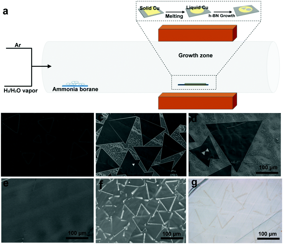 | ||
| Fig. 1 (a) Schematic diagram showing the CVD setup. Typical SEM images of h-BN grown on liquid Cu with different growth time (min): (b) 50, (c) 60, (d) 70, (e) 80, (f) 90. (g) Optical image of h-BN on Cu foil. | ||
Fig. 1b–d show the scanning electron microscopy (SEM) images of h-BN grown at 1140 °C with Ar (20 sccm) and H2 (3 sccm bubbling water) flow at different growth time (50, 60 and 70 min). The h-BN domains obtained have a triangular shape, indicating that these domains are single crystals with nitrogen-terminated zigzag edges.3–11 These domains nucleate on the surface, and then grow larger with time, reflecting a nucleation and growth mechanism. The 70 min growth results in single h-BN domains with a size of up to 330 μm (Fig. 1d), which is 3–5 times larger compared to the best results previously reported on Cu and Cu-Ni alloy foil.3,13 The average growth rate is estimated to be 5–10 μm min−1, which is considerably higher than previously reported results. On further increasing the growth time, these individual domains gradually cover the whole surface of liquid Cu, and finally merge into continuous films (Fig. 1e). On further increasing the growth time (90 min), few-layered h-BN domains are formed around the coalescent area (grain boundaries) of triangular h-BN domains (Fig. 1f and g). Large-sized h-BN domains and transferred h-BN film on the SiO2/Si substrate are also observed by optical imaging (Fig. S1, ESI†).
The role of water vapor in h-BN growth was investigated by systematically changing the amount of water vapor carried by H2 gas flow in the h-BN growth system while keeping other parameters unchanged. Fig. 2a shows the SEM image of h-BN grown without adding water (see details in Table S1, ESI†). It is clearly shown that the nucleation density of h-BN grains is so high that the average size of triangular-shaped h-BN domains is about 3–5 μm. In contrast, the nucleation density of h-BN is dramatically reduced in the case of adding water vapor carried by 3, 10 and 20 sccm H2 gas as shown in Fig. 2b–d. Interestingly, while the nucleation densities are similar in three cases (Fig. S2b, ESI†), the sizes of h-BN domains show a peak as a function of the amount of water vapor (Fig. S2a, ESI†). This result reflects that the growth rate is reduced when excess water vapor is used. In addition, a clear shape evolution of h-BN domains with the amount of water vapor used is observed. Considering the perfect triangle as a reference of geometric objects, the straight edges of triangular h-BN domains change to negatively curved edges when the amount of water vapor increases.
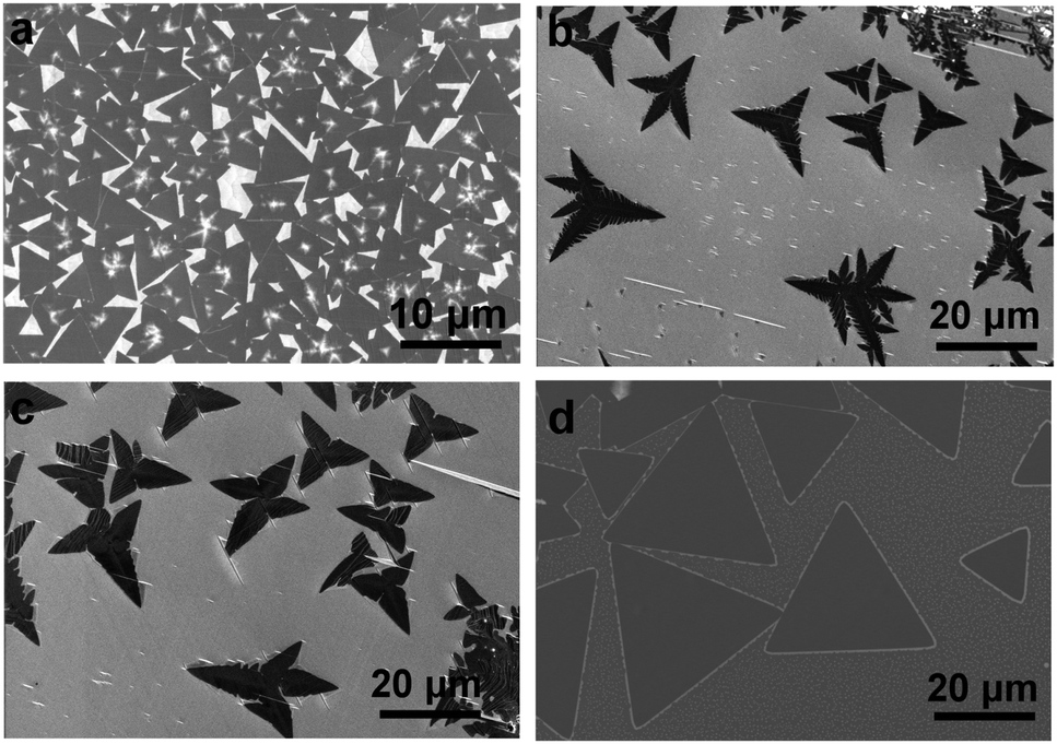 | ||
| Fig. 2 SEM images of h-BN grown under different amounts of water vapor carried by H2: (a) 0, (b) 3, (c) 10, (d) 20 sccm. | ||
The above experiments reveal that the main role of water vapor in h-BN growth is to reduce the nucleation density of h-BN, which can be reasonably explained by the chemistry occurring between water vapor and B atoms at high temperature. Indeed, the water vapor is capable of reacting with the B element to generate B2O2 vapor at the growth temperature of h-BN17 (eqn (1)), thus providing a means to tune the overall net nucleation and growth of h-BN.
| B(s) + H2O(g) → B2O2(g) + H2(g) | (1) |
To reveal the etching effect of water vapor on the growth of h-BN, we investigated the etching behavior of h-BN film under different etching environments. Fig. S3 (ESI†) shows the SEM images under different etching conditions (see the details in Table S2, ESI†). When Ar gas was applied in the etching process, no obvious etching was found in the h-BN film (Fig. S3a, ESI†). In contrast, by using mixed water vapor and Ar as etchants, most of the h-BN film was etched away, leaving some straight lines and dendritic patterns on the surface (Fig. S3b, ESI†). In addition, the use of pure H2 (3 sccm) and mixed H2/water vapor (3 sccm H2 gas bubbling water) for etching h-BN film was also compared as shown in Fig. S3c and d (ESI†), respectively. When using H2 as the etching agent, some white particles appear on the surface, but no etched patterns are observed. However, when using water vapor as the etching agent, triangle-shaped holes on h-BN film appear, which is similar to our previous results.6 All of these results demonstrate that water vapor is capable of etching h-BN at the growth temperature.
This effect is apparently similar to that of simply tuning the amount of precursor. However, from a microscopic point of view, the transport or diffusion process of active building blocks is partly affected by the density and distribution of active building blocks, other surface adsorbed species and impurities on the surface. In this sense, the etching effect provided by water vapor could produce a different unique “environment” that leads to tunable nucleation and growth of h-BN domains otherwise inaccessible by the common means of changing the amount of precursors. As there are two competing etching and growth processes, an optimal condition is expected to be found in terms of control over nucleation density or h-BN domain sizes. In the present case, while the use of excess water can reduce the nucleation density, the growth rate is compromised, which results in a relative small h-BN domain size. The role of water vapor in shaping h-BN domain geometry is discussed below.
Extensive characterization of samples was performed. Auger electron spectroscopy (AES) mappings for h-BN domains and film on Cu (Fig. 3a and Fig. S4, ESI†) confirm that the distribution of B and N elements is homogeneous. The corresponding AES spectra show the characteristic B (KLL) and N (KLL) peaks located at 176 and 385 eV, respectively.18 The atomic B/N ratio of samples is 1.07 based on X-ray photoelectron spectroscopy (XPS) measurements, in which B1s and N1s peaks are situated at 190.54 and 398.02 eV, respectively (Fig. 3c and d).3–13 Moreover, the B1s peak can be divided into one shoulder peak, located at 191.69 eV, reflecting the substitution of the N atom by O in the h-BN lattice.19 The N1s also can be divided into a peak, located at 399.74 eV, which can be attributed to the formation of N–O and B–N–O bonds in the h-BN film.19 The O substitution in the h-BN lattice is commonly found in CVD grown h-BN, and is statistically unavoidable.
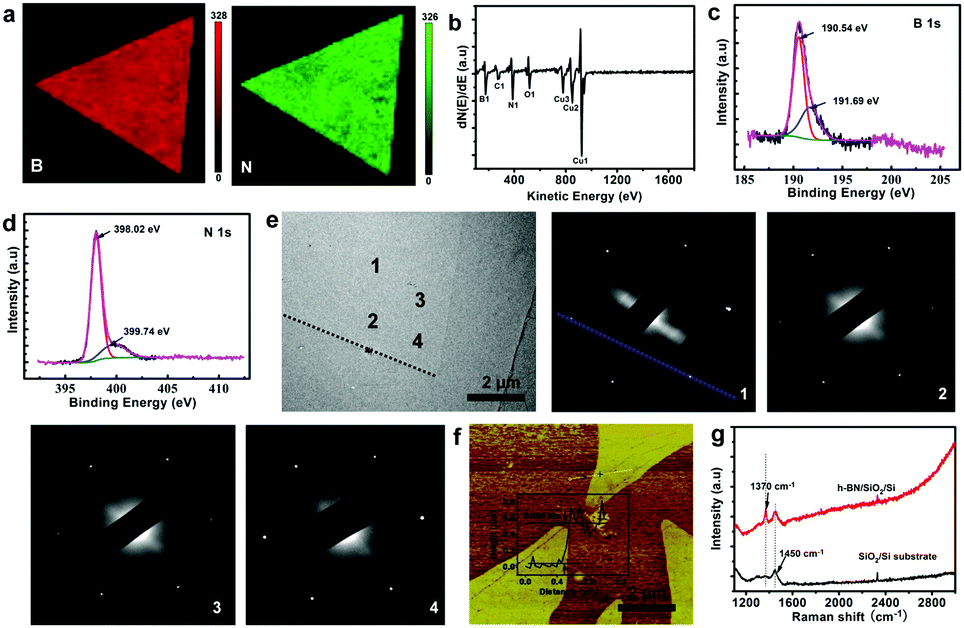 | ||
| Fig. 3 (a) The corresponding B (KLL) and N (KLL) Auger electron maps. (b) AES spectra taken from the areas shown in (a). (c) and (d) The corresponding XPS spectra of B 1s and N 1s, respectively. (e) A typical TEM image of a triangular h-BN domain on the holey carbon grid and SAED patterns recorded on different locations labelled in the TEM image. (f) AFM image of h-BN transferred onto the SiO2/Si substrate. (g) The Raman spectra taken from h-BN domains transferred onto the SiO2/Si substrate. | ||
The selected area electron diffraction (SAED) of a h-BN domain measured at different locations (Fig. 3e) shows a set of characteristic six-fold symmetric spots, indicating that the h-BN domains are single crystals. The zigzag orientation derived from the SAED pattern (indicated by the dashed line in Fig. 3e) is nearly parallel to the edge of the triangle, indicating that the edges of the h-BN domain are along the zigzag orientations, consistent with previous results.5 The thickness of transferred h-BN domains measured by atomic force microscopy (AFM) on the SiO2/Si substrate is about 0.465 nm (Fig. 3f), consistent with the h-BN monolayer.3–11 The scanning tunneling microscopy (STM) image of the sample (Fig. S5, ESI†) reveals the atomic-scale structure with the characteristic h-BN lattice constants of 0.253 nm, which are consistent with the theoretical data.20 The Raman spectrum of the h-BN film on a SiO2/Si substrate shows a peak at ∼1369 cm−1, originating from the B–N bond stretching of the h-BN monolayer (Fig. 3g).21 The peak near 1450 cm−1 is from the third-order transverse optic mode of the silicon substrate.22
As the geometric shape of single crystal 2D materials directly reflects their internal and edge structures, controlling the shape provides a myriad of opportunities for exploring edge structure- or orientation-related physics. Remarkably, in analogy to the case of shape engineering of graphene crystals,23 the manipulation of the Ar/H2 flow rate ratio in our water-assisted growth method results in a continuous change of h-BN domain shapes (Fig. 4, see also details in Table S3, ESI†). With gradually increasing Ar![[thin space (1/6-em)]](https://www.rsc.org/images/entities/char_2009.gif) :H2 ratio, the shapes of h-BN domains change from regular triangle, positively curved triangle, regular hexagon, polygon, finally to circle. These patterns together with those obtained by tuning the amount of water vapor (Fig. 2) form a set in which there is a clear geometric rule connecting different shapes (Fig. 4i). Regardless of the detailed microscopic growth processes, the geometric shape change reflects the gradual change of growth rates along different directions that are becoming more and more isotropic as a function of modulation of experimental parameters. Careful analysis of these conditions reveals that the concentrations of h-BN building blocks are gradually increasing for the shapes grown from the left to the right (Fig. 4i). Therefore, it can be speculated that this situation together with a “unique environment” affecting the diffusion process is responsible for the observed shape modulation. More generally, the shape change can be envisaged as due to competition among the different growth rates along different directions associated with specific edge energy, the amount of precursor supply and kinetic surface diffusion process. It should be mentioned that some of h-BN shapes have been observed previously using various methods such as changing the temperature of the h-BN precursor and the distance between grown substrate and precursors. Compared to these observations,14,24 this work provides an expanded family of patterns and a key explanation based on the amount of the precursors supported by experiments, which is essentially capable of predicting the previous results based on the corresponding experimental conditions.
:H2 ratio, the shapes of h-BN domains change from regular triangle, positively curved triangle, regular hexagon, polygon, finally to circle. These patterns together with those obtained by tuning the amount of water vapor (Fig. 2) form a set in which there is a clear geometric rule connecting different shapes (Fig. 4i). Regardless of the detailed microscopic growth processes, the geometric shape change reflects the gradual change of growth rates along different directions that are becoming more and more isotropic as a function of modulation of experimental parameters. Careful analysis of these conditions reveals that the concentrations of h-BN building blocks are gradually increasing for the shapes grown from the left to the right (Fig. 4i). Therefore, it can be speculated that this situation together with a “unique environment” affecting the diffusion process is responsible for the observed shape modulation. More generally, the shape change can be envisaged as due to competition among the different growth rates along different directions associated with specific edge energy, the amount of precursor supply and kinetic surface diffusion process. It should be mentioned that some of h-BN shapes have been observed previously using various methods such as changing the temperature of the h-BN precursor and the distance between grown substrate and precursors. Compared to these observations,14,24 this work provides an expanded family of patterns and a key explanation based on the amount of the precursors supported by experiments, which is essentially capable of predicting the previous results based on the corresponding experimental conditions.
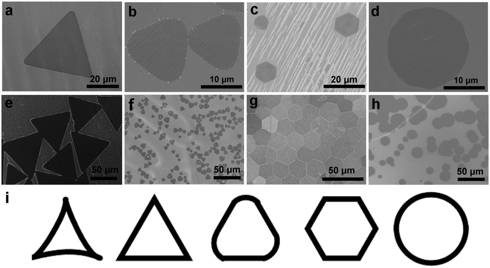 | ||
| Fig. 4 (a–d) SEM images of various-shaped h-BN domains grown on liquid Cu surface under different Ar/H2 ratios (20/3, 100/3, 200/3 and 400/3, respectively). (e–h) The corresponding large-scale SEM images of the above ones. (i) Schematic diagram of various geometric shapes found in experiments. | ||
The structure of hexagon-shaped h-BN domains was also confirmed to be single crystals by SAED measurements (Fig. S6, ESI†), indicating that the whole set of hexagon-shaped h-BN domains essentially has the nature of single crystals, which is similar to the case of graphene crystal patterns. Based on the previous studies and our TEM results, the triangle-shaped h-BN domains have three N-terminated zigzag edges, and the hexagon consists of alternating N- and B-terminated edge structures. In the case of polygon, some chiral edges between zigzag and armchair with N- or B-termination can be derived simply by geometric consideration. In addition, it is interesting to note that hexagonal h-BN domains with similar sizes pack into a compact ordered structure in analogy to the case of graphene grown on liquid Cu surface (Fig. 4g).25
For electronic applications, graphene/h-BN/300 nm SiO2/Si FET devices were fabricated. Device fabrication procedures were similar to that previously reported,23 and electrical transport measurements were conducted in ambient conditions. Fig. 5a shows a typical Raman spectrum of the graphene/h-BN/SiO2/Si, indicating that the single crystal graphene is well-crystallized with few defects.26 Fig. S7 (ESI†) shows the typical optical image of the graphene/h-BN film device. Fig. 5b displays the transfer curve of typical graphene/SiO2/Si and graphene/h-BN back-gate FET, which shows p-type behavior similar to our previous results for the graphene sample on the h-BN film substrate.27 In these cases, the use of h-BN films as a dielectric layer exhibits the improvement of graphene carrier mobility and the downshift of Dirac point compared to that of SiO2/Si as a dielectric substrate. The calculated hole mobility is about 5263 cm2 V−1 s−1, higher than our previous tested results using h-BN as a dielectric layer.28
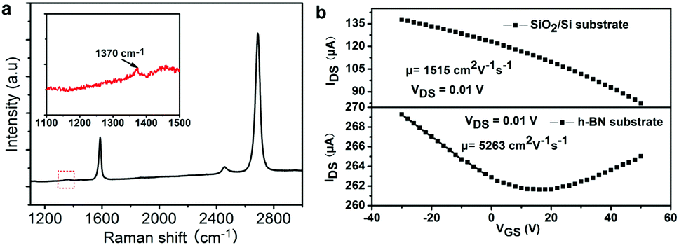 | ||
| Fig. 5 (a) Raman spectra of graphene transferred on the h-BN/SiO2/Si substrate. The inset shows the Raman characteristic peak of h-BN. (b) Transfer curves of graphene/SiO2/Si and graphene/h-BN films FET. | ||
Conclusions
In summary, we demonstrate a water-assisted CVD approach that allows the effective modulation of nucleation and growth processes, leading to a fast growth of large-sized single crystal h-BN domains and a tuning of h-BN geometric shapes. This method provides a much broader range for controlling h-BN growth compared with the existing methods.Experiments
H-BN growth
Cu foils were first cleaned using acetic acid, ethanol, and ultrapure water (1:1:1) for 10 min to remove the native oxide and impurities. Then h-BN was directly grown on liquid Cu surface under atmospheric pressure CVD. Prior to growth, a certain amount of ammonia borane was placed in a quartz boat, away from the center of the furnace. Once the growth temperature (1140 °C) was obtained, the precursor was heated to 60–90 °C by a heating belt. After a certain period of growth time (typically 80–90 min), the single-crystal h-BN domains and monolayer films were synthesized. After growth, both the heating furnace and the heating belt were quickly cooled down to room temperature.
Transfer
As-grown h-BN grains or continuous monolayer films on Cu surface were transferred onto the 300 nm SiO2/Si substrate and TEM grid for further characterization by PMMA-assisted electrochemical bubbling method. Briefly, the front side of the h-BN film on Cu foil was covered with PMMA, followed by immersing the sample in an aqueous solution of 1 M NaOH for electrochemical delamination. The PMMA/h-BN/Cu foil and a bare Pt mesh were utilized as an anode and a cathode, respectively. The bubbling transfer was performed under a constant electrolytic voltage of 5 V for 2–4 min. After peeling off the PMMA/h-BN film from the Cu foil, it was rinsed with deionized water several times in order to remove residual NaOH solution. Finally, films were transferred onto desired substrates and PMMA was removed by acetone rinsing.Characterization
The samples were characterized by XPS spectroscopy, Raman spectroscopy (Renishaw inVia Plus, with laser excitation at 514 nm and spot size of 1–2 μm), Auger electron spectroscopy (AES), optical microscopy, scanning electron microscopy (SEM, Hitachi S-4800, 1 and 15 kV), atomic force microscopy (AFM, Veeco Nanoman VS in the tapping mode), transmission electron microscopy (Tecnai G2 F20 U-TWIN, operated at 200 kV), AES (PHI-700), electrical measurements (Keithley, SCS-4200) and scanning tunneling microscopy (STM, Veeco Nanoscope IIIa with a Pt–Ir alloy tip).Acknowledgements
This work was supported by the National Basic Research Program of China (2016YFA0200101, 2013CB933500), the National Natural Science Foundation of China (21273243, 51233006, 61390500 and 21633012), Beijing Municipal Science & Technology Commission (Z161100002116025), and Chinese Academy of Sciences and the Strategic Priority Research Program of the Chinese Academy of Sciences (XDB12030100).Notes and references
- Y. Kubota, K. Watanabe, O. Tsuda and T. Taniguchi, Science, 2007, 317, 932–934 CrossRef CAS PubMed.
- A. Geim and I. Grigorieva, Nature, 2013, 499, 419–425 CrossRef CAS PubMed.
- X. Song, et al. , Nano Res., 2015, 8, 3164–3176 CrossRef CAS.
- S. Kim, et al. , Nano Lett., 2013, 13, 933–941 CrossRef CAS PubMed.
- J. Yin, et al. , Small, 2015, 11, 4497–4502 CrossRef CAS PubMed.
- L. Wang, et al. , Adv. Mater., 2015, 27, 4858–4864 CrossRef CAS PubMed.
- M. H. Khan, et al. , Sci. Rep., 2015, 5, 7743 CrossRef CAS PubMed.
- Y. Gao, et al. , ACS Nano, 2013, 7, 5199–5206 CrossRef CAS PubMed.
- J. Park, et al. , ACS Nano, 2014, 8, 8520–8528 CrossRef CAS PubMed.
- Z. Liu, et al. , Nat. Commun., 2014, 4, 2541 Search PubMed.
- S. Caneva, et al. , Nano Lett., 2015, 15, 1867–1875 CrossRef CAS PubMed.
- S. M. Kim, et al. , Nat. Commun., 2015, 6, 8662 CrossRef CAS PubMed.
- G. Lu, et al. , Nat. Commun., 2015, 6, 6160 CrossRef CAS PubMed.
- R. Y. Tay, et al. , Nano Lett., 2014, 14, 839–846 CrossRef CAS PubMed.
- Q. Wu, et al. , Sci. Rep., 2015, 5, 16159 CrossRef CAS PubMed.
- W. Auwärter, H. U. Suter, H. Sachdev and T. Greber, et al. , Chem. Mater., 2004, 16, 343–345 CrossRef.
- J. Li, J. Li, Y. Yin, Y. Chen and X. Bi, et al. , Nanotechnology, 2013, 24, 365605 CrossRef PubMed.
- C. Zhang, et al. , Nat. Commun., 2015, 6, 6519 CrossRef CAS PubMed.
- P. R. Kidambi, et al. , Chem. Mater., 2014, 26, 6380–6392 CrossRef CAS PubMed.
- S. Joshi, et al. , Nano Lett., 2012, 12, 5821–5828 CrossRef CAS PubMed.
- R. V. Gorbachev, et al. , Small, 2011, 7, 465–468 CrossRef CAS PubMed.
- G. Han, et al. , ACS Nano, 2013, 7, 10129–10138 CrossRef CAS PubMed.
- B. Wu, et al. , NPG Asia Mater., 2013, 5, e36 CrossRef CAS.
- Y. J. Stehle, et al. , Chem. Mater., 2015, 27, 8041–8047 CrossRef CAS.
- S. Y. Cho, et al. , Nanoscale, 2015, 7, 12820–12827 RSC.
- D. M. Hoffman, G. L. Doll and P. C. Eklund, et al. , Phys. Rev. B: Condens. Matter Mater. Phys., 1984, 30, 6051–6056 CrossRef CAS.
- A. C. Ferrari, et al. , Phys. Rev. Lett., 2006, 97, 187401 CrossRef CAS PubMed.
- L. Wang, et al. , Adv. Mater., 2014, 24, 1559–1564 CrossRef PubMed.
Footnote |
| † Electronic supplementary information (ESI) available: Further details of the annealing and oxidation procedures, STM measurements, AFM imaging and Raman spectroscopy measurements. See DOI: 10.1039/c7qm00100b |
| This journal is © the Partner Organisations 2017 |