High-quality organohalide lead perovskite films fabricated by layer-by-layer alternating vacuum deposition for high efficiency photovoltaics†
Mohammad Mahdi
Tavakoli
ab,
Abdolreza
Simchi
b,
Xiaoliang
Mo
*c and
Zhiyong
Fan
*a
aDepartment of Electronic and Computer Engineering, Hong Kong University of Science and Technology, Clear Water Bay, Kowloon, Hong Kong SAR, China. E-mail: eezfan@ust.hk
bDepartment of Materials Science and Engineering and Institute for Nanoscience and Nanotechnology, Sharif University of Technology, 14588 Tehran, Iran
cDepartment of Materials Science, Fudan University, Shanghai 200433, P. R. China. E-mail: xlmo@fudan.edu.cn
First published on 6th February 2017
Abstract
Herein, we present, for the first time, a new procedure to fabricate stoichiometric, uniform, and highly crystalline lead perovskite thin films based on a multi-step vapor deposition technique. In this process, the perovskite film is prepared by layer-by-layer alternating (LBLA) vacuum deposition of PbI2 and methylammounium iodide (MAI). In comparison to the common two-step deposition (TSD) approach, the novel LBLA evaporation process yields thin films with much improved uniformity in terms of composition, morphology, and surface quality. X-ray photoelectron spectroscopy and inductively coupled plasma mass spectrometry show that the I/Pb ratio of the LBLA film is 2.92 ± 0.03, which indicates a more precise stoichiometric composition of organometallics as compared with TSD with an I/Pb ratio of 2.76 ± 0.06. X-ray diffraction and time-resolved photoluminescence measurements also demonstrate higher crystallinity and a longer lifetime for the LBLA films, as compared with the films fabricated by the conventional TSD method. Atomic force microscopy indicates 36% improvement in the surface smoothness as well. The better film quality leads to ∼20% improved power conversion efficiency in bulk heterojunction solar devices, primarily owing to a higher fill factor and current density.
Introduction
Organic–inorganic perovskite solar cells have attained remarkable light harvesting efficiency since their early manifestation in 2012, with a recently certified world record efficiency of 22.1%.1–4 Besides the high power conversion efficiency (PCE), their fabrication processes are facile and of relatively low-cost, indicating their strong potential for building scalable and cost-effective photovoltaic modules.5–8 Generally, there are two approaches to prepare perovskite films, namely the solution process and vacuum deposition.9–12 Using these techniques, the perovskite film can be synthesized by a one- or two-step process. The two-step deposition (TSD) process usually produces a perovskite film with a higher quality regarding the morphology of the layer, pinhole defects, and uniformity.3,13 The other advantages of the vacuum deposition technique compared with the solution process include the scalability, reproducibility, and purification of the precursors during the evaporation process.9 Recent studies14–18 have shown that the TSD process possesses better control over MAI evaporation, which is a critical step in the fabrication of high-quality perovskite films. By employing an extra amount of PbI2, improved solar device performance can also be attained.20Although TSD has some advantages such as precise-control over the thickness, composition and morphology of the perovskite films, MAI evaporation is still challenging for attaining precise control over the deposition rate and the deposited thickness.3 In fact, MAI evaporation is often not a reproducible and repeatable process. On the other hand, during annealing of the films at elevated temperatures, CH3NH3I molecules in the upper layer are evaporated and detached from the surface due to their weak bonds.19 Consequently, the annealed perovskite films fabricated by the TSD approach may not gain a stoichiometric composition. Therefore, controlling the MAI evaporation rate and attaining a stoichiometric composition are bottle-neck technical challenges especially for future large scale production19–22 affecting the film quality and finally the photovoltaic device performance. To address these challenges associated with the high vapor pressure of MAI,3 we have developed a multi-step process based on layer-by-layer alternating (LBLA) vacuum deposition of PbI2 and MAI materials in sequential stages. The quality of deposited films with regard to the composition, crystallinity, morphology, uniformity and smoothness is presented and compared with thin films prepared by the TSD process. It is shown that the novel LBLA vacuum deposition technique yields uniform and smooth films with large grain sizes and stoichiometric composition (the Pb/I ratio is close to 3). The photovoltaic characterization results show that the perovskite solar cells fabricated by the LBLA procedure possess a higher fill factor (FF) and current density leading to ∼20% improvement in the overall device PCE. Our results demonstrate that the LBLA-prepared device has a maximum fill factor of 83% which is as high as the maximum FF reported in the literature.23
Results and discussion
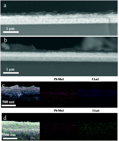
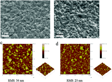
The two-step deposition of organohalides suffers from drawbacks of poorly controlled deposition rate and MAI volatility during the post-annealing stage, which lead to non-stoichiometric films with a non-uniform microstructure. We have utilized LBLA deposition of the perovskite materials using vacuum processing (ESI,† Fig. S1) to prepare films with higher quality regarding the chemical composition, morphology, and smoothness. Fig. 1 presents the cross-sectional SEM images of the films prepared by TSD (Fig. 1a) and LBLA (Fig. 1b) methods in a backscattered mode. The thickness of the perovskite films is ∼350 nm. As is seen, the LBLA perovskite film is more uniform and smoother than the TSD layer. Composition variations along different layers (without annealing of perovskite films), as analyzed by EDS mapping, are shown in Fig. 1c and d. After vacuum deposition, the sandwich structure of the LBLA film and the two-layer structure of the TSD one were annealed at 100 °C for 10 min to complete the reaction and improve the crystallinity of the perovskite film. The results of EDS mapping demonstrate that the LBLA prepared film shows a uniform distribution of Pb and I elements, which is better than the TSD one.Further characterization was performed on the top surfaces of the films to study the details of the grain structure and surface roughness of the films. Top-view SEM images of the films are shown in Fig. 2a. As is seen, both layers are compact but the grain size of the LBLA film is larger and more uniform than that of the TSD one (ESI,† Fig. S2). The average grain sizes of perovskite films fabricated by LBLA and TSD methods are 480 ± 70 nm and 330 ± 90 nm, respectively. It is notable that these values were estimated from the image analysis24,25 of 4 SEM images of each method. The AFM images shown in Fig. 2b indicate that the surface of the LBLA film is smoother than that of the TSD layer. The root-mean-square (RMS) surface roughness of the perovskite films is estimated to be 25 nm (for LBLA) and 34 nm (for TSD) in the area of 10 μm × 10 μm.
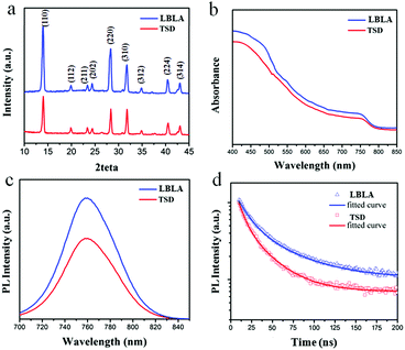
The phase and compositional characteristics as well as the optical properties (absorption and emission) of the deposited films were studied by different techniques. The results are summarized in Fig. 3 and explained in the following. The XRD patterns shown in Fig. 3a present the characteristic peaks of the crystalline perovskite structure, in agreement with the literature.12 The XRD analysis indicates that organohalide lead perovskite (CH3NH3PbI3) is formed upon annealing. Meanwhile, the characteristic peaks of the LBLA film are more intensive than TSD, which highlights the higher crystallinity of the layer with the same thickness. From the absorbance spectra (Fig. 3b), it is conclusive that both films have an optical bandgap of ∼1.59 eV, although the absorbance of the LBLA film is slightly higher. The steady-state and transient photoluminescence (PL) spectra of the perovskite films are shown in Fig. 3c and d, respectively. Both films exhibit 780 nm steady-state emissions with stronger peak intensity for the LBLA film, however with the same detector integration time, the LBLA film shows a higher excitonic peak than the TSD film. The results of TRPL measurements indicate that the LBLA film has a longer carrier lifetime (25.6 ns) than the TSD (16.3 ns). The values of curve fitting parameters are shown in Table S1 (ESI†). Therefore, the carrier transport in the perovskite film prepared by the LBLA method is expected to be faster with a lower recombination rate. In order to further determine the composition of the vacuum deposited films, XPS and ICP-MS tests were employed. The results of XPS are shown in Fig. 4a and b. Fig. 4a reveals the differences in the chemical state (composition) of the films prepared by the two different methods. Peak analysis determines the variations in the intensity of Pb 4f and I 3d lines, which can indicate the differences in the I/Pb molar ratio. Details of Pb 4f spectra with two separate contributions of 4f7/2 and 4f5/2 peaks are shown in Fig. 4b. The strong peaks located at 138.7 eV and 143.6 eV correspond to Pb 4f7/2 and Pb 4f5/2, respectively. These peaks are consistent with the binding energy of lead halides (PbX2, X: Cl, Br, I) and Pb in the perovskite structure.26–29 The smaller peaks located at 137 eV and 142.3 eV are ascribed to metallic lead (Pb0).30–34 It is notable that the intensity of these peaks for the LBLA films is low and negligible compared with those of the TSD perovskite film. This observation reveals that the amount of metallic lead in the perovskite film is significantly reduced by employing the LBLA process. The results of XPS elemental analysis as well as of ICP-MS spectrometry are shown in Table 1. The I/Pb molar ratio in the LBLA film is higher than in the TSD layer and is very close to 3.
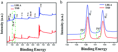 | ||
| Fig. 4 (a) XPS survey spectra and (b) Pb 4f5/2 and 4f7/2 detailed spectra of CH3NH3PbI3 perovskite films fabricated by TSD and LBLA evaporation processes. | ||
| Method | I/Pb from XPS | I/Pb from ICP-MS |
|---|---|---|
| TSD | 2.79 ± 0.16 | 2.73 ± 0.07 |
| LBLA | 2.94 ± 0.12 | 2.91 ± 0.05 |
Therefore, the LBLA procedure produces films with a composition closer to the stoichiometric perovskite structure, which is a great advantage for the charge carrier transport.20
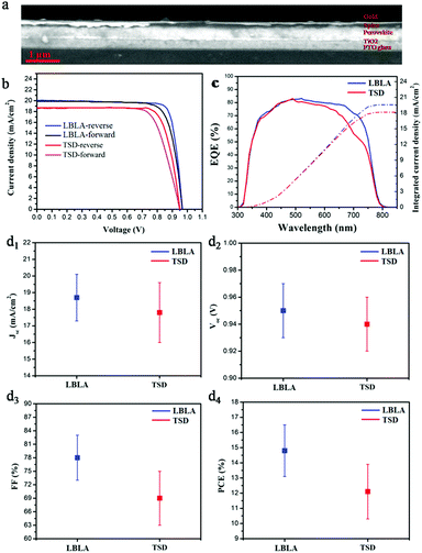
To study the effect of the vacuum deposition technique on the electronic properties of the perovskite films, bulk heterojunction solar cells were fabricated and their PCEs were determined. The crystalline perovskite films were deposited on TiO2-coated FTO glass and the hole transport layer (Spiro) was spin-coated. Finally, 100 nm-thick gold was thermally-evaporated as an electrode to complete the device architecture. Fig. 5a shows the cross-sectional SEM image of the photovoltaic device made from the perovskite film prepared by the LBLA deposition process. As is shown, the perovskite film is very smooth and uniform. Fig. 5b presents the current density–voltage (J–V) curves under AM 1.5G illumination with forward and reverse scan directions. The figures of merit for the perovskite devices (best devices) are shown in Table 2.
| Device | V oc (V) | J sc (mA cm−2) | FF (%) | PCE (%) |
|---|---|---|---|---|
| TSD-reverse | 0.95 | 18.7 | 75 | 13.3 |
| TSD-forward | 0.95 | 18.5 | 72 | 12.6 |
| LBLA-reverse | 0.96 | 20.1 | 83 | 15.9 |
| LBLA-forward | 0.96 | 19.9 | 81 | 15.4 |
From the results, we can see that the device fabricated by the LBLA method shows a slightly lower hysteresis effect than its counterpart, due to its better perovskite composition and larger grain size.35,36 The LBLA-prepared device (champion cell) exhibits a high fill factor of 82% with a current density of 20 mA cm−2. The PCE is 15.6%, which is 20% higher than that of the TSD cell (12.9%). Notably, these values are the average results of forward and reverse scan directions. Fig. 5c shows the external quantum efficiency (EQE) spectra of the best perovskite solar cells fabricated by LBLA and TSD techniques. After integration of the EQE spectra and the AM 1.5G solar photon flux in the range of 300 nm to 850 nm, maximum current densities of 19.6 mA cm−2 and 18.2 mA cm−2 for LBLA and TSD perovskite cells were obtained, respectively. The LBLA-prepared device demonstrates a higher Jsc (calculated from EQE) than the TSD cell, which is in good agreement with the J–V measurements. In addition to the best J–V measurement results, the average values of 20 devices prepared by both techniques are presented in Fig. 5d1–d4. The average results of J–V measurements indicate that the LBLA-prepared device shows a high FF (78%) and Jsc (18.7 mA cm−2), which are 13% and 5% higher than the TSD-prepared one, respectively. This results in a high average efficiency of 14.8% for the LBLA device. This achievement is attributed to the better crystallinity, larger grain size, more stoichiometric composition, less Pb0 in the film, and more uniform and smoother surfaces.
To further study the LBLA-prepared device, electrochemical impedance spectroscopy (EIS) was employed. The results of the EIS test (Nyquist curves) under dark conditions are shown in Fig. 6. In these curves, Z′ and Z′′ are the real and imaginary parts of the cell impedance, respectively. As shown, the LBLA device has a smaller semicircle radius than the TSD cell, indicating the lower charge-transfer resistance. The estimated values of the ohmic resistance and charge-transfer resistance (using the inset circuit in Fig. 6) of devices prepared by LBLA are 22.3 and 267.6 Ohm, respectively, which are lower than those of the corresponding TSD device, 24.8 and 321.7 Ohm, respectively. This confirms the better quality of the LBLA perovskite film, and its lower recombination rate and higher short-circuit current density.
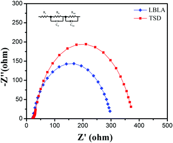 | ||
| Fig. 6 EIS spectra of perovskite solar cells prepared by LBLA and TSD approaches. The inset is the equivalent circuit used for modeling of impedance data. | ||
Conclusions
In summary, we present a novel technique to prepare high-quality perovskite films through a layer-by-layer alternating (LBLA) vacuum deposition process. The effects of LBLA processing on the film morphology, grain structure, smoothness, and composition of perovskite films based on organohalide lead were systematically studied. It was shown that the chemical composition of the LBLA film was very close to the stoichiometric value (I/Pb molar ratio of 3) with a negligible amount of metallic lead. The LBLA process produced uniform films with smooth surface roughness (RMS = 25 nm) and a large grain size of 480 ± 70 nm. As compared with the perovskite films prepared by a common two-step deposition (TSD) process, the quality of the LBLA films is remarkably better. Consequently, the LBLA film exhibited a longer carrier lifetime (25.6 ns) than the TSD layer (16.3 ns). Photovoltaic performance measurements showed a higher fill factor and current density with better external quantum efficiency for the LBLA devices. Solar cell with a PCE of 16.6% was fabricated that had 20% higher performance with lower hysteresis than the TSD devices. This improvement was achieved through preparing better quality perovskite films with a longer charge carrier lifetime by LBLA vacuum processing.Experimental
Materials
Acetone, acetonitrile, methanol, isopropyl alcohol, diethyl ether, and Triton X-100 were purchased from Merck, Germany. Lead(II) iodide powder (PbI2, 99%), methylamine (33 wt% in ethanol, Sigma-Aldrich), hydroiodic acid (57 wt% in water, Sigma-Aldrich), Spiro-OMeTAD (Lumtec, Taiwan), Li-bis(trifluoromethanesulfonyl)imide (Sigma-Aldrich), titanium diisopropoxide bis(acetylacetonate) solution (75% in 2-propanol, Sigma-Aldrich), 4-tert-butylpyridine (tBP, Sigma Aldrich), and titanium tetrachloride (Sigma-Aldrich) were used as received without further purification.Synthesis of the organohalide precursor
The MAI solution was prepared by the reaction of 38 mL of methylamine (33 wt% in ethanol, Sigma-Aldrich) and 40 mL of hydroiodic acid (57 wt% in water, Sigma-Aldrich) in a 250 mL round-bottom flask in an ice bath, followed by stirring for 2 h. Crystallization of MAI was performed using a rotary evaporator at 50 °C to remove the solvent (the pressure was 7 × 10⁻³ mbar). The obtained whitish product was re-dissolved in absolute ethanol and precipitated by diethyl ether. Finally, MAI powder was collected and dried at 60 °C under vacuum (7 × 10⁻³ mbar) overnight.Preparation of transparent conductive substrates for thin film deposition
The FTO substrates (Hartford Glass, USA) were sequentially cleaned by ultra-sonication (Sonicor S-101) for 30 min in different solvents including acetone (Merck), 3 vol% Triton X-100-containing deionized (DI) water (Millipore, 18 MΩ cm), isopropanol, and DI water. The substrates were then dried under an air gas flow. A 50 nm-thick TiO2 compact layer was deposited on the FTO glass through spin-coating (4000 rpm for 40 s) of a 0.15 mM solution of titanium diisopropoxide bis(acetylacetonate) (75% in 2-propanol, Sigma-Aldrich). Afterwards, the substrates were dried at 150 °C for 20 min and sintered at 500 °C for 30 minutes in air. Then, the TiO2-coated substrates were immersed in 40 mM TiCl4 (Aldrich) aqueous solution for 30 min at 70 °C and annealed at 500 °C for 30 min.Vacuum deposition of perovskite films
Organohalide lead perovskite films were vacuum deposited on the surface of TiO2-coated FTO glass using TSD and LBLA evaporation processes. First, 1 g of lead iodide (PbI2) and 0.5 g of methylammonium iodide (CH3NH3I) powders were loaded into two separate quartz crucibles surrounded by two tungsten wire heaters. The crucibles and tungsten heaters were installed in a thermal evaporator. Then the TiO2 coated FTO substrate was mounted on the vacuum chamber 20 cm above the source materials. After mounting the substrates on the chamber stage, the precursors were evaporated under a vacuum of 4 × 10⁻⁶ mbar. The deposition rates of PbI2 and MAI were fixed at 0.1–0.2 nm s−1 and 0.6–1 nm s−1, respectively. The deposition rate was controlled by a quartz sensor and calibrated according to the thickness of the PbI2 and MAI films. In order to fabricate high-quality perovskite films by the TSD process, the relative composition of MAI to PbI2 and the total thickness of the film were optimized to 1![[thin space (1/6-em)]](https://www.rsc.org/images/entities/char_2009.gif) :
:![[thin space (1/6-em)]](https://www.rsc.org/images/entities/char_2009.gif) 1 molar ratio and 350 nm, respectively, based on a previous study.3 The film was then annealed at 100 °C for 1 h in an argon atmosphere. In the LBLA process, PbI2 and MAI were deposited alternatingly in a total of 10 steps. In each of the 5 PbI2 deposition steps, 24 nm thick PbI2 was deposited. And in each of the 5 MAI deposition steps, 68 nm thick MAI was deposited according to our thickness monitor setup and the selected material parameters. Therefore after deposition the total thickness of the film is the same as the TSD process (350 nm). A schematic of the deposition strategy to prepare high-quality films is shown in Fig. S1, ESI.† The sandwich organic/inorganic structure encapsulates the volatile MAI material and provides a short diffusion path to homogenize upon the high-temperature annealing post-processing.
1 molar ratio and 350 nm, respectively, based on a previous study.3 The film was then annealed at 100 °C for 1 h in an argon atmosphere. In the LBLA process, PbI2 and MAI were deposited alternatingly in a total of 10 steps. In each of the 5 PbI2 deposition steps, 24 nm thick PbI2 was deposited. And in each of the 5 MAI deposition steps, 68 nm thick MAI was deposited according to our thickness monitor setup and the selected material parameters. Therefore after deposition the total thickness of the film is the same as the TSD process (350 nm). A schematic of the deposition strategy to prepare high-quality films is shown in Fig. S1, ESI.† The sandwich organic/inorganic structure encapsulates the volatile MAI material and provides a short diffusion path to homogenize upon the high-temperature annealing post-processing.
Materials characterization
The morphology and thickness of perovskite films were studied by field-emission scanning electron microscopy (FESEM, JEOL-7100F). The phase composition and crystallinity of the films were investigated by X-ray diffraction (Bruker D8 X-ray diffractometer) with Cu Kα radiation and inductively coupled plasma mass spectrometry (ICP-MS, PerkinElmer). A Varian Cary 500 spectrometer was employed for optical absorption. Atomic force microscopy (AFM) measurements were obtained using a Veeco Dimension 3100, operating in tapping mode. Steady-state and transient photoluminescence measurements were performed on an Edinburgh Instruments FLS920P fluorescence spectrometer. The excitation source is a picosecond pulsed diode laser (EPL-670, 671.4 nm excitation wavelength, pulse width 62.8 ps). To remove the stray light hitting the R928T detector, a long pass filter with a 730 nm cut-on wavelength was positioned in the emission path. Time-correlated single photon counting was employed to record the photoluminescence decay curves. In order to calculate the carrier life-time, an exponential function with the form of I(t) = B1![[thin space (1/6-em)]](https://www.rsc.org/images/entities/char_2009.gif) exp(−t/τ1) was fitted to the decay curve, where τ1 and B1 are the life-time constant and the amplitude of the exponential component. For X-ray photoelectron spectroscopy (XPS), a hemispherical analyzer with an Al Kα X-ray source (1486.6 eV) at 10−9 mbar was utilized.
exp(−t/τ1) was fitted to the decay curve, where τ1 and B1 are the life-time constant and the amplitude of the exponential component. For X-ray photoelectron spectroscopy (XPS), a hemispherical analyzer with an Al Kα X-ray source (1486.6 eV) at 10−9 mbar was utilized.
Fabrication and characterization of photovoltaic devices
To prepare the hole transport layer on the perovskite films, a solution of Spiro-OMeTAD (80 mg ml−1 chlorobenzene), 17.5 μL of Li-bis(trifluoromethanesulfonyl)imide (Li-TFSI)/acetonitrile (500 mg mL−1), and 28.5 μL of 4-tert-butylpyridine (tBP) was spin-coated at 3000 rpm for 40 s. After drying the Spiro layer in a dry box overnight, 100 nm-thick gold was thermally evaporated (0.08 nm s−1) as the top electrode. The device performance was measured using a solar spectrum at AM 1.5G, which is simulated using an Abet Class AAB Sun 2000 simulator with an intensity of 100 mW cm−2 after calibration with a KG5-filtered Si reference cell. The current density–voltage (J–V) measurements were recorded using a 2400 Series SourceMeter (Keithley, USA) instrument. The sweep ranges were between 0 and +1.2 V, with a step size of 0.02 V and a delay time of 150 ms at each point. External quantum efficiency (EQE) measurements versus wavelength were performed using a constant white light bias of nearly 5 mW cm−2 and an Oriel QE-PV-SI (Newport Corporation).Acknowledgements
This work was supported by the General Research Fund (project 612113) from the Hong Kong Research Grant Council, the Hong Kong Innovation and Technology Fund (project ITS/362/14FP) from the Innovation and Technology Commission, Center for 1D/2D Quantum Materials and State Key Laboratory on Advanced Displays and Optoelectronics at HKUST and National Natural Science Foundation of China (project 51672231).Notes and references
- M. Saliba, T. Matsui, K. Domanski, J. Y. Seo, A. Ummadisingu, S. M. Zakeeruddin, J. P. Correa-Baena, W. R. Tress, A. Abate, A. Hagfeldt and M. Grätzel, Science, 2016, 354, 206–209 CrossRef CAS PubMed.
- J. W. Lee, H. S. Kim and N. G. Park, Acc. Chem. Res., 2016, 49, 311–319 CrossRef CAS PubMed.
- M. M. Tavakoli, K. H. Tsui, Q. Zhang, J. He, Y. Yao, D. Li and Z. Fan, ACS Nano, 2015, 9, 10287–10295 CrossRef CAS PubMed.
- H. J. Snaith, J. Phys. Chem. Lett., 2013, 4, 3623–3630 CrossRef CAS.
- B. R. Sutherland, S. Hoogland, M. M. Adachi, C. T. Wong and E. H. Sargent, ACS Nano, 2014, 8, 10947–10952 CrossRef CAS PubMed.
- M. M. Tavakoli, A. Tayyebi, A. Simchi, H. Aashuri, M. Outokesh and Z. Fan, J. Nanopart. Res., 2015, 17, 1–13 CrossRef CAS.
- M. Liu, M. B. Johnston and H. J. Snaith, Nature, 2013, 501, 395–398 CrossRef CAS PubMed.
- W. Qiu, M. Buffière, G. Brammertz, U. W. Paetzold, L. Froyen, P. Heremans and D. Cheyns, Org. Electron., 2015, 26, 30–35 CrossRef CAS.
- M. M. Tavakoli, R. Tavakoli, Z. Nourbakhsh, A. Waleed, U. S. Virk and Z. Fan, Adv. Mater. Interfaces, 2016, 3, 1500790 CrossRef.
- M. M. Tavakoli, L. Gu, Y. Gao, C. Reckmeier, J. He, A. L. Rogach, Y. Yao and Z. Fan, Sci. Rep., 2015, 5, 14083 CrossRef PubMed.
- J. Burschka, N. Pellet, S. J. Moon, R. Humphry-Baker, P. Gao, M. K. Nazeeruddin and M. Grätzel, Nature, 2013, 499, 316–319 CrossRef CAS PubMed.
- M. M. Tavakoli, Q. Lin, S. F. Leung, G. C. Lui, H. Lu, L. Li, B. Xiang and Z. Fan, Nanoscale, 2016, 8, 4276–4283 RSC.
- H. S. Kim, J. W. Lee, N. Yantara, P. P. Boix, S. A. Kulkarni, S. Mhaisalkar, M. Grätzel and N. G. Park, Nano Lett., 2013, 13, 2412–2417 CrossRef CAS PubMed.
- J. Teuscher, A. Ulianov, O. Müntener, M. Grätzel and N. Tétreault, ChemSusChem, 2015, 8, 3847–3852 CrossRef CAS PubMed.
- G. E. Eperon, V. M. Burlakov, P. Docampo, A. Goriely and H. J. Snaith, Adv. Funct. Mater., 2014, 24, 151–157 CrossRef CAS.
- M. M. Tavakoli, R. Tavakoli, S. Hasanzadeh and M. H. Mirfasih, J. Phys. Chem. C, 2016, 120, 19531–19536 CAS.
- L. Wang, C. McCleese, A. Kovalsky, Y. Zhao and C. Burda, J. Am. Chem. Sci., 2014, 136, 12205–12208 CrossRef CAS PubMed.
- M. A. Green, A. Ho-Baillie and H. J. Snaith, Nat. Photonics, 2014, 8, 506–514 CrossRef CAS.
- G. Longo, L. Gil-Escrig, M. J. Degen, M. Sessolo and H. J. Bolink, Chem. Commun., 2015, 51, 7376–7378 RSC.
- M. M. Tavakoli, A. Simchi, Z. Fan and H. Aashuri, Chem. Commun., 2016, 52, 323–326 RSC.
- S. Wang, L. K. Ono, M. R. Leyden, Y. Kato, S. R. Raga, M. V. Lee and Y. Qi, J. Mater. Chem. A, 2015, 3, 14631–14641 CAS.
- L. Etgar, P. Gao, Z. Xue, Q. Peng, A. K. Chandiran, B. Liu, M. K. Nazeeruddin and M. Grätzel, J. Am. Chem. Sci., 2012, 134, 17396–17399 CrossRef CAS PubMed.
- C. H. Chiang and C. G. Wu, Nat. Photonics, 2016, 10, 196–200 CrossRef CAS.
- M. M. Tavakkoli and S. M. Abbasi, Mater. Des., 2013, 46, 573–578 CrossRef CAS.
- M. M. Tavakoli, R. Tavakoli, P. Davami and H. Aashuri, J. Comput. Electron., 2014, 13, 425–431 CrossRef CAS.
- R. Lindblad, D. Bi, B. Park, J. Oscarsson, M. Gorgoi, H. Siegbahn, M. Odelius, E. M. J. Johansson and H. Rensmo, J. Phys. Chem. Lett., 2014, 5, 648–653 CrossRef CAS PubMed.
- M. Scrocco, Phys. Rev. B: Condens. Matter Mater. Phys., 1982, 25, 1535 CrossRef CAS.
- J. Moulder, W. Stickle, P. Sobol and K. Bomben, Phys. Electron. Div., Eden Prairie, 1995 Search PubMed.
- M. M. Tavakoli, H. Aashuri, A. Simchi and Z. Fan, Phys. Chem. Chem. Phys., 2015, 17, 24412–24419 RSC.
- C. Hinnen, C. N. V. Huong and P. Marcus, J. Electron Spectrosc. Relat. Phenom., 1995, 73, 293–304 CrossRef CAS.
- C. D. Wagner and J. A. Taylor, J. Electron Spectrosc. Relat. Phenom., 1980, 20, 83–93 CrossRef CAS.
- B. Conings, L. Baeten, C. De Dobbelaere, J. D'Haen, J. Manca and H. G. Boyen, Adv. Mater., 2014, 26, 2041–2046 CrossRef CAS PubMed.
- M. M. Tavakoli, H. Aashuri, A. Simchi, S. Kalytchuk and Z. Fan, J. Phys. Chem. C, 2015, 119, 18886–18895 CAS.
- M. M. Tavakoli, A. Simchi and H. Aashuri, Mater. Chem. Phys., 2015, 156, 163–169 CrossRef CAS.
- Y. Zhao and K. Zhu, J. Phys. Chem. C, 2014, 118, 9412–9418 CAS.
- W. Nie, H. Tsai, R. Asadpour, J. C. Blancon, A. J. Neukirch, G. Gupta, J. J. Crochet, M. Chhowalla, S. Tretiak, M. A. Alam and H. L. Wang, Science, 2015, 347, 522–525 CrossRef CAS PubMed.
Footnote |
| † Electronic supplementary information (ESI) available. See DOI: 10.1039/c6qm00379f |
| This journal is © the Partner Organisations 2017 |

