DOI:
10.1039/C6QM00335D
(Research Article)
Mater. Chem. Front., 2017,
1, 1229-1244
Graphene oxide co-doped with dielectric and magnetic phases as an electromagnetic wave suppressor†
Received
24th November 2016
, Accepted 21st January 2017
First published on 23rd January 2017
Abstract
The fabrication of thin multilayer polymer nanocomposite films and their judicious arrangement in a sandwich structure to attenuate incoming electromagnetic (EM) radiation, mostly by absorption, is discussed herein. Two key properties (reasonably high conductivity, with high dielectric loss and magnetic permeability) were targeted here by using multiwall nanotubes (MWCNTs) and BaTiO3/Fe3O4 (BT/Fe) co-doped graphene oxide (GO) sheets to design soft functional nanocomposites using bi-component blends of PC (polycarbonate) and PVDF (polyvinylidene fluoride). High dielectric loss and magnetic permeability were achieved by uniformly distributing BT and Fe nanoparticles on the huge specific surface area provided by the GO sheets. The MWCNTs were non-covalently modified to exfoliate the nanotubes and to get a well-connected structure of the blend components. The MWCNTs were thoroughly characterized by TEM, UV-vis, fluorescence emission, Raman and TGA. This surface modification of the MWCNTs also helps with their specific localization in the continuous bi-component blends. BT and Fe were co-doped onto the GO sheets by a well-designed step-by-step synthesis protocol, and the product can facilitate the absorption of incoming EM radiation. This hybrid structure was thoroughly characterized by various microscopic and spectroscopic techniques. By following a sequential mixing protocol, the BT/Fe co-doped GO sheets can be specifically localized in the PC components of the blends while the MWCNTs localize in the PVDF phase through a process driven by thermodynamics. This provides excellent heterogeneous boundaries with multiple scattering within the engineered nanostructures, in addition to retaining the conducting network and the associated dielectric loss properties. The resultant local field variation of such boundaries and the presence of highly lossy materials readily enhance the EM attenuation coefficient. The bulk compositions exhibited a high shielding effectiveness (SE) of −35 dB at 18 GHz (>85% absorption), and when rationally stacked into a multilayer architecture with absorption–multiple reflection–absorption pathways, the SE was further enhanced to −46 dB for a thin shield of 0.9 mm thickness. Such a high SE indicates >99.99% attenuation of the incoming EM radiation. This new-generation EM suppressor, distinguished by its multifunctionality and tunable dielectric and magnetic properties, hence offers an amendable, cost-effective replacement to existing solutions.
Introduction
Electromagnetic interference (EMI) is created by the widespread use of specialized devices and the pervasive utilization of supplementary electronic devices, as a side effect. These transmitted electromagnetic waves meddle with the hardware of adjacent equipment and manifest as disturbances during the operation of devices, which can lead to the inconsistent operation of or glitches in accurate equipment. On account of this, protecting devices from external EM radiation has become imperative. Along these lines, and with the aim of constraining EM radiation, some shielding technology must be designed to protect the internals of devices from their immediate surroundings. Within this framework, substantial endeavours have been made during the last couple of decades to develop lightweight, corrosion resistant and simple-to-manufacture EM screening materials.1–6
EM wave screening is for the most part determined by two essential parameters. It is mostly accomplished by reflection, where mobile charges are carried by free electrons and can associate with the existing EM field. Otherwise, the waves are absorbed and dissipated into heat due to the local field variation of different dielectric and magnetic properties. Metals are the primarily used protecting materials, however they have poor properties such as being difficult to handle, having poor adaptability, having huge weights and being susceptible to corrosion. As an alternative, the use of conducting polymer nanocomposites has increased impressively due to their having the following attributes: light weights, ease of processing, auxiliary adaptabilities, and corrosion resistance.7–12
Moreover, in contrast with metals that are controlled at bigger length scales are polymer nanocomposites which assimilate complex components that can be related to the chain of importance of scales. This is on the grounds that charge is transported by plasmons (quasi-particles) as opposed to free electrons, nano-electromagnetism is the system by which the macroscopic behaviours of nanocomposites are investigated as opposed to established electromagnetism, and the development of multiple channels in the network where tunnelling effects are important.13
Be that as it may, with the specific end goal of accomplishing high electrical conductivity, high concentrations of conducting filler particles are regularly included, which frequently reduce the general mechanical properties of the composites. In relation to this, a progressive change was realized via carbon nanotubes (CNTs) owing to their ability to form interconnected structures at low loadings due to their high aspect ratio. However, in the composites a slender layer of protecting polymer hinders the charge transport mechanism. Different techniques have been proposed to address the issues identified, with the goal of acquiring a uniform scattering of CNTs in a polymer network. It is obvious that the electrical conductivity of CNTs relies upon π-conjugation. It is also well established that upon the functionalization of CNTs by other substances, this π-conjugation can be influenced. Chemical functionalization permits the outfitting of various functional moieties on the surface of CNTs, which can be used to improve the interfacial adhesion with the framework, and therefore the large scale modification of CNTs is essential.14–20
However, graphene has already garnered an enormous reputation in terms of its wide-ranging applications recently, as a perfect alternative to 1D CNTs. In the last decade, graphene has been at the forefront of materials research, and is remarkable due to its outstanding conductivity and thermal, electronic, and mechanical properties.21–28 A handful of recent investigations incorporating magnetic particle doped 3D graphene and other carbonic nanocapsules in EMI applications have been reported, most notably by Jian et al.,29 Tang et al.30 and Singh et al.31 However, the high mass fractions of fillers in these reported systems bring with them additional shortfalls, viz. reduced processability and productivity.32–36 Moreover, the reported systems have largely overlooked the aspect of interconnected network formation in the matrices. Not only materials with sufficient electrical conductivity, but also dielectric and magnetic lossy materials greatly influence the EM shielding efficiency by absorbing the incident EM wave which is dissipated into heat.37–41 Careful control over the mechanical properties and EM shielding ability are the primary concerns of designing modern light weight flexible shielding materials.
In light of the existing literature, we observed that either individual particles or hybrid particles in a matrix result in efficient shielding, however this is limited to a certain frequency bandwidth. Moreover, most of the literature reports a combination of either conducting or lossy (dielectric/magnetic) nanoparticles to suppress EM radiation. This results in either reflection or absorption dominated shielding. Herein, we have designed a unique hybrid particle (BT/Fe co-doped GO sheets) by a two-step protocol to provide particular dielectric and magnetic properties, which in combination with conducting MWCNTs results in significant shielding effectiveness dominated mostly by absorption. Furthermore, this design yielded composites without compromising the flexibility and the mechanical properties of the composites. Blending two immiscible polymers (here PC and PVDF) could be a superior choice for fabricating EM shielding materials, as nanomaterials with different characteristics can be localized in different components through the selective harnessing of surface functional groups. By non-covalently conjugating the MWCNTs with an anthracene derivative, enhanced conductivity was achieved at lower fractions of MWCNTs through an exfoliated network in PVDF; this achieved one of the key targets i.e. relatively high conductivity. On the other hand we have designed a unique hybrid of a BT/Fe co-doped-graphene derivative, to selectively localize it in PC following a sequential mixing protocol during compounding. The incorporation of hybrid and lossy nanomaterials into the system not only enhances the shielding effectiveness but also alters the overall shielding mechanism. By localizing the particles in different components, the volume electrical conductivity was retained, leading to further suppression of the incoming EM radiation. The success of the individual soft composites further led us to design a multilayer stack (of 0.9 mm thickness) following a rational arrangement which resulted in exceptional shielding effectiveness when compared with the individual layers.
Experimental section
Materials
PVDF (Kynar-761, with a Mw of 440![[thin space (1/6-em)]](https://www.rsc.org/images/entities/char_2009.gif) 000 g mol) was kindly provided by Arkema. Polycarbonate (Lexan-143R) was obtained from Sabic (MFI 11 g/10 min). Pristine MWCNTs (length 1.5 μm and diameter 9.5 nm) were procured from Nanocyl SA (Belgium). BaTiO3 (BT, average particle size 100 nm), FeCl3, FeSO4·7H2O, N,N′-dicyclohexylcarbodiimide (DCC), 4-dimethylaminopyridine (DMAP), 9-anthracenecarboxaldehyde (ACA), 3-hydroxybenzaldehyde, (3-aminopropyl)triethoxysilane (APTS), and hydrazine hydrate were procured from Sigma Aldrich. Analytical grades of chloroform, 28% ammonia solution, ethanol, N,N-dimethylformamide graphite flakes, H2SO4, H3PO4, and tetrahydrofuran were obtained from commercial sources.
000 g mol) was kindly provided by Arkema. Polycarbonate (Lexan-143R) was obtained from Sabic (MFI 11 g/10 min). Pristine MWCNTs (length 1.5 μm and diameter 9.5 nm) were procured from Nanocyl SA (Belgium). BaTiO3 (BT, average particle size 100 nm), FeCl3, FeSO4·7H2O, N,N′-dicyclohexylcarbodiimide (DCC), 4-dimethylaminopyridine (DMAP), 9-anthracenecarboxaldehyde (ACA), 3-hydroxybenzaldehyde, (3-aminopropyl)triethoxysilane (APTS), and hydrazine hydrate were procured from Sigma Aldrich. Analytical grades of chloroform, 28% ammonia solution, ethanol, N,N-dimethylformamide graphite flakes, H2SO4, H3PO4, and tetrahydrofuran were obtained from commercial sources.
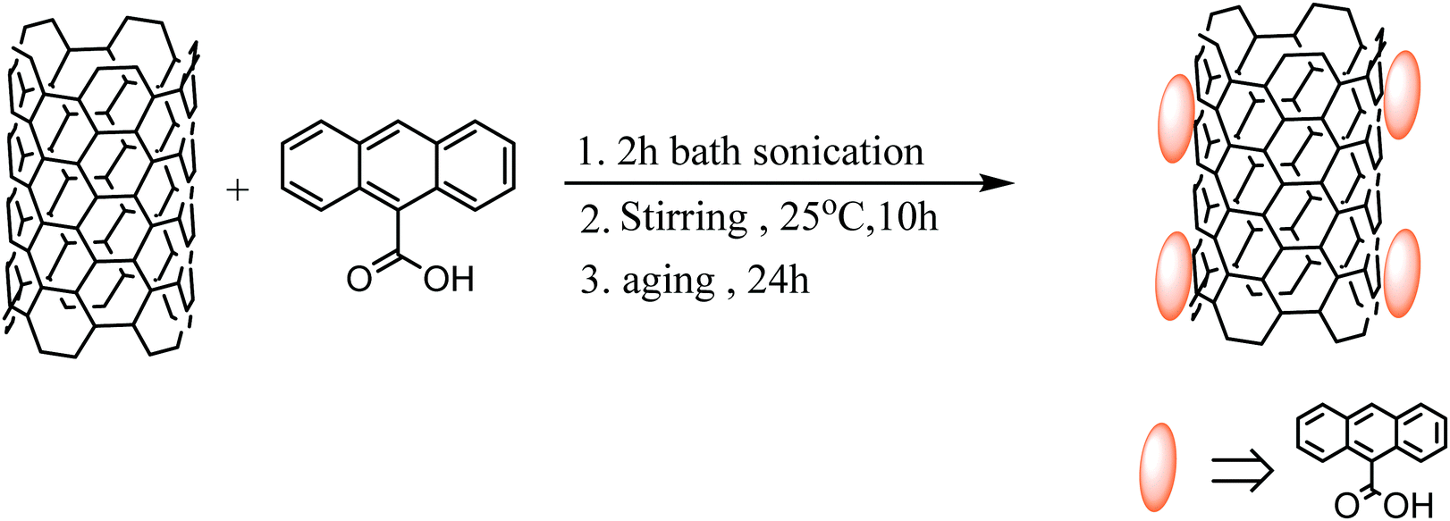
Preparation of ACA modified MWCNTs
Anthracene based organic compounds generally have very high thermal and chemical stabilities and low volatilities which make them superior for various applications. Anthracene based ACA has a very strong interaction with MWCNTs due to π–π stacking originating from the extended π-conjugation of the anthracene moiety and delocalized π-clouds in the MWCNTs. So the surfaces of the MWCNTs were modified here by the non-covalent attachment of ACA molecules in a typical weight ratio of 2:1. Initially the mixture was sonicated in an ethanol medium for 2 h at room temperature and then vigorously stirred overnight. After ageing for 24 h, finally the mixture was centrifuged and washed several times until the complete removal of unbound ACA molecules was achieved. This removal process was systematically guided by a UV-vis spectroscopic technique. The mixture was then vacuum dried at 80 °C overnight. The detailed procedure is schematically represented here in Scheme 1.
 |
| | Scheme 1 Preparation of ACA modified MWCNTs. | |
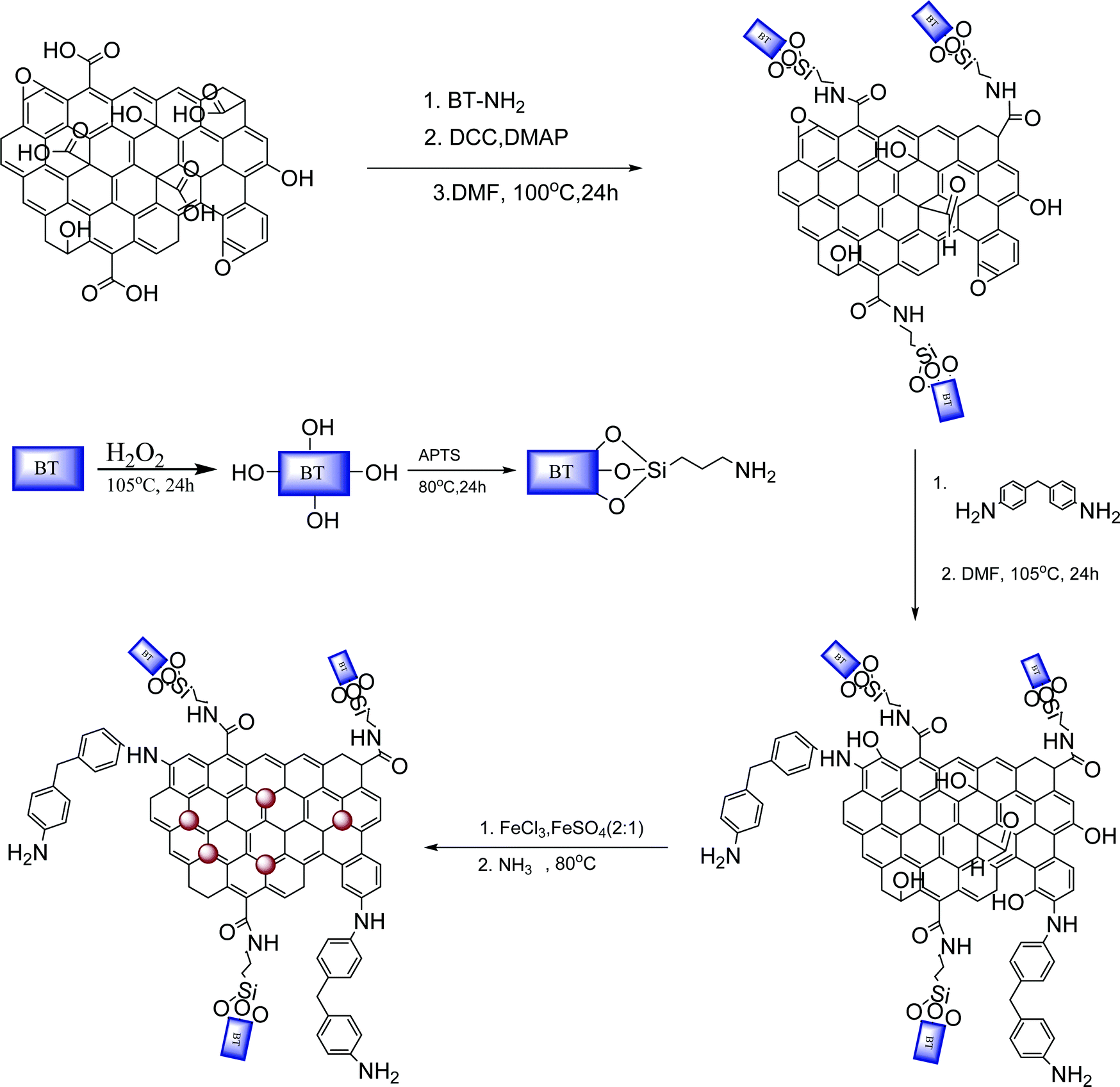
Preparation of MDA modified BT/Fe co-doped GO sheets
The preparation of the MDA modified BT/Fe co-doped GO sheets consists of three different steps. GO and BT-NH2 were initially synthesized as reported in our previous work.42 For the covalent attachment of BT nanoparticles on to GO sheets, typically 5 wt% BT-NH2 was treated with GO in a DMF solution at 100 °C 24 h. After cooling to room temperature the resultant mixture was washed several times and then dried under vacuum at 80 °C overnight. The dry powder obtained was then dispersed again in DMF by bath sonication and treated with MDA for 24 h at 105 °C. Then the resultant mixture was washed with excess DMF and acetone and vacuum dried at 80 °C overnight. The obtained powder was dispersed in water, (2:1) FeCl3:FeSO4 was added and then this mixture was treated with excess NH3 solution for 4 h at 80 °C. Finally the mixture was centrifuged and washed several times with DI water and then vacuum dried at 80 °C overnight. The detailed procedure is schematically illustrated in Scheme 2.
 |
| | Scheme 2 Preparation of MDA modified BT/Fe co-doped GO sheets. | |
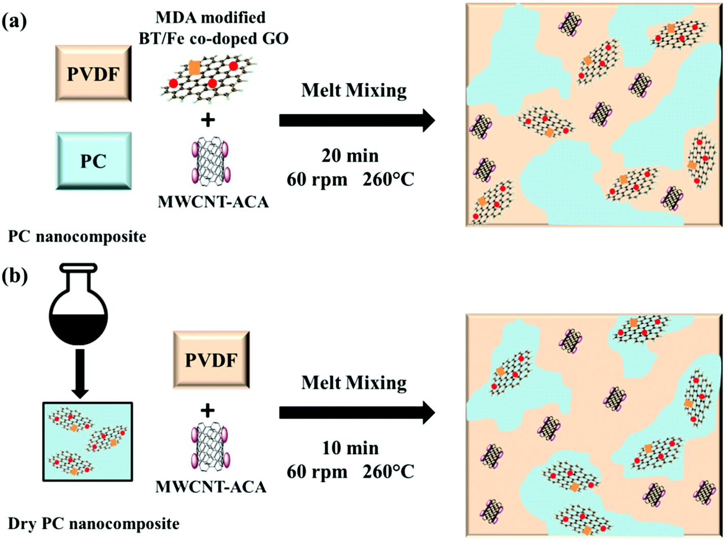
Preparation of blends
All the blends with different nanoparticles were prepared by using a Hake minilab-II melt compounder under a nitrogen atmosphere at 260 °C with a 60 rpm rotational speed for 20 min. Some of the blends where all the nanoparticles are in the PVDF phase (driven by thermodynamics) were prepared by adding all the components together into the melt compounder. In order to localize the BT/Fe co-doped GO sheets in the PC phase a strategic protocol was adopted. More precisely, PC nanocomposites containing BT/Fe co-doped GO sheets were initially prepared prior to mixing with the PVDF/MWCNTs during melt mixing. It is envisaged that MDA modified BT/Fe co-doped GO sheets can react with the ester groups of PC via a nucleophilic substitution mechanism (see Fig. S1, ESI†) thereby preventing them from migrating to the PVDF component during melt-mixing. All the blends developed here contain 3 wt% conducting MWCNTs and 5 wt% BT/Fe co-doped GO sheets modified with MDA. Here we have briefly explained the detail blend preparation procedure in Scheme 3.
 |
| | Scheme 3 (a) PC/PVDF blend where both nanomaterials are in the PVDF, (b) PC/PVDF blend where MWCNT-ACA is in the PVDF phase and MDA modified BT/Fe co-doped GO is in PC. | |
Construction of multilayer assembly
Thin layers of the polymer blends were prepared by compression molding at 230 °C. The melt blended samples were used for compression molding. After obtaining all the layers of the specific composites (each of 0.30 mm thickness), they were stacked again by compression molding, however, this time at a much lower temperature (150 °C) and applying much less pressure (105 Pascal). Generally the melting temperature of neat PVDF is near 170 °C, and hence by adopting this strategy the layers can be made to fuse together without melting the individual layers.
Characterization
Transmission electron micrographs and HAADF (high angle annular dark field) images were procured utilizing a FEI Technai F30 instrument operated at an acceleration voltage of 300 kV. EDS mapping was additionally done using the same instrument. A Sirion XL30 FEG SEM with an acceleration voltage of 10 kV was utilized to determine the morphologies of the PC/PVDF blends. A PerkinElmer GX FT-IR instrument was utilized to obtain FT-IR spectra. A Shimadzu UV-1800 spectrophotometer was used to study the UV-vis absorption spectra and a Hitachi F-2500 spectrofluorometer with a 1 cm quartz cell was used for fluorescence measurements. For fluorescence measurements, the excitation and emission slits with a band pass of 2.5 nm were used for all the samples. The PMT (photomultiplier tube) voltage was kept at 700 V and the scan speed was 5 nm s−1. The magnetic properties of the synthesized nanoparticles were assessed using a Lakeshore Vibratory Sample Magnetometer (VSM) with an applied force of −8000 to 8000 Oe at room temperature. Raman spectra were recorded using a LabRam HR (UV) system. X-ray diffraction data was recorded utilizing an XPERT Pro from PANalytical. A Cu Kα radiation source (l = 1.5406 Å, 40 kV and 30 mA) was used to decipher the XRD profiles of the different nanoparticles. The room temperature electrical conductivity of the blend was determined utilizing an Alpha-N Analyser, Novocontrol (Germany) in a frequency range from 0.1 Hz to 10 MHz. UTM was utilized for assessing the mechanical properties of the different blends. A 5 mm min−1 cross head speed was utilized. Preceding the estimation, dumbbell-formed specimens were set up by a compression moulding machine. EM interference shielding was measured by utilizing an Anritsu MS4642A VNA. A Damaskos MT-07 co-axial connector was utilized and a KEYCOM waveguide was utilized to measure the shielding efficiency of the multilayer architecture.
Result and discussion
Characterization of different synthesized nanoparticles
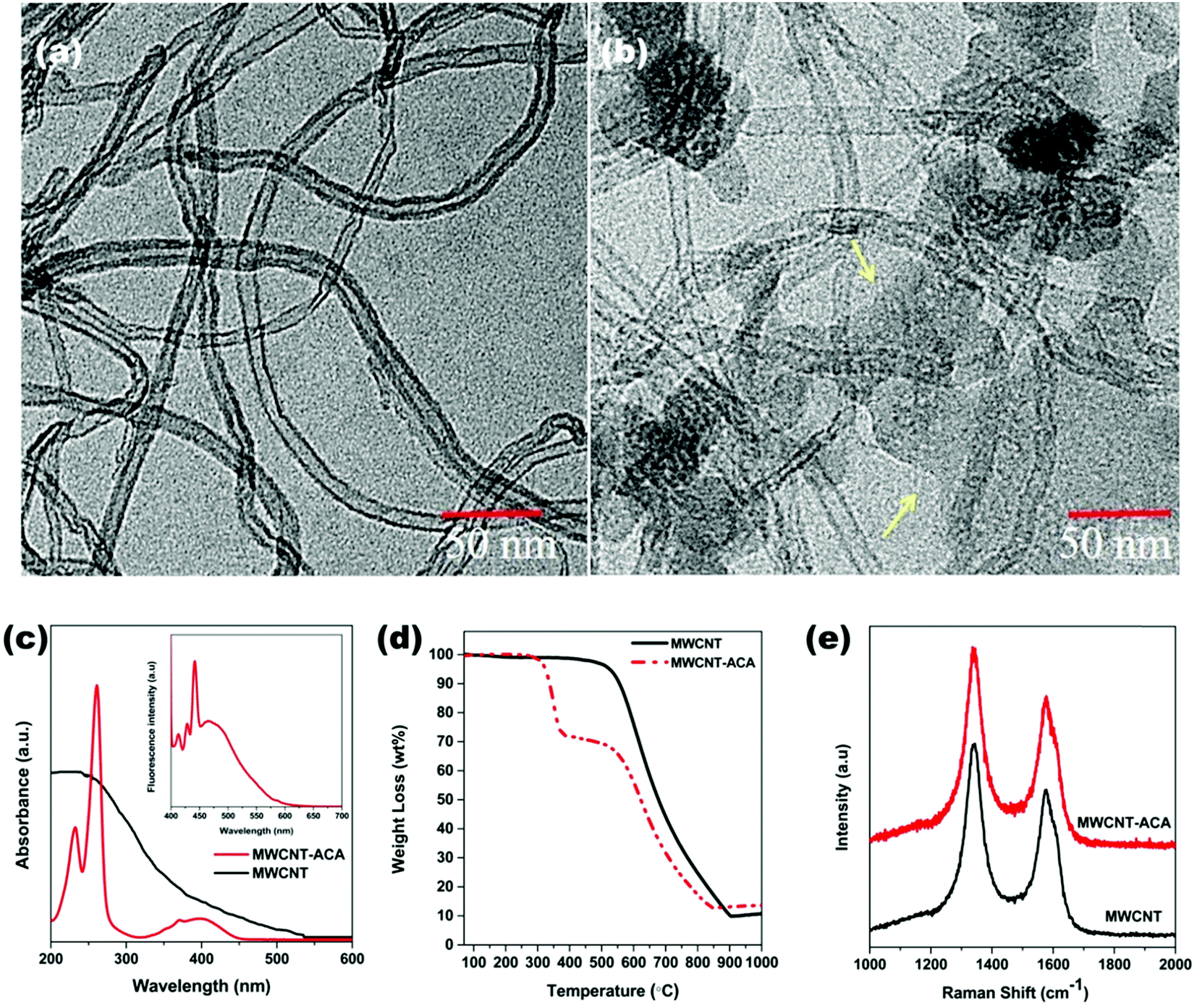
The successful attachment of ACA molecules on the surfaces of MWCNTs was examined using TEM images (Fig. 1a and b). The π–π interaction is the main driving force of such attachment, which originates from the extended π-conjugation of the anthracene moiety and the delocalized π-clouds in the MWCNTs. The layers, which are marked by arrows in Fig. 1b, exhibited the presence of ACA molecules, which are absent in Fig. 1a, where only MWCNTs are shown. The successful attachment process can also be proved by using UV-vis spectroscopy and fluorescence emission spectroscopy (Fig. 1c). It is obvious that MWCNTs don't show any signal in the UV-vis spectra due to the lack of functional groups on their surfaces. However after the attachment of ACA molecules on the surfaces, two characteristic peaks are discerned. It is important to note that the complete removal of unbound ACA molecules was confirmed using UV-vis spectra as shown in Fig. S2 (ESI†). The peak at 261 nm corresponds to the π–π* transition and the peak at 396 nm corresponds to the n–π* transition originating from the non-covalently attached ACA molecules. Furthermore, these conjugated molecules can also exhibit strong fluorescence emission spectra in the 390 nm region while MWCNTs do not have any such emission in their spectra (inset of Fig. 1c). So it is clear that the non-covalent attachment of ACA to MWCNTs through π–π stacking was done successfully. We also determined that the final attachment of ACA molecules is nearly 20%, from thermo-gravimetric analyses in air (Fig. 1d). This experiment also focused on the thermal stability of the type of conjugation present here. We have further employed Raman spectra for analysing the structural changes in MWCNTs while undergoing this non-covalent attachment process (Fig. 1e). It is observed that the ID/IG ratio, which is a measure of the amount of defect structure, is ca. 1.25 for ACA modified MWCNTs while neat MWCNTs have ca. 1.24. So this type of non-covalent attachment can be seen to maintain the structural integrity of MWCNTs which is essential for efficient charge transportation phenomena.
 |
| | Fig. 1 TEM images of (a) MWCNT, (b) MWCNT-ACA (arrows indicate the layer of ACA molecules). (c) UV-Vis absorption spectra (inset shows fluorescence spectra of MWCNT-ACA), (d) TGA analysis plot in air and (e) Raman spectra of MWCNT and MWCNT-ACA. | |
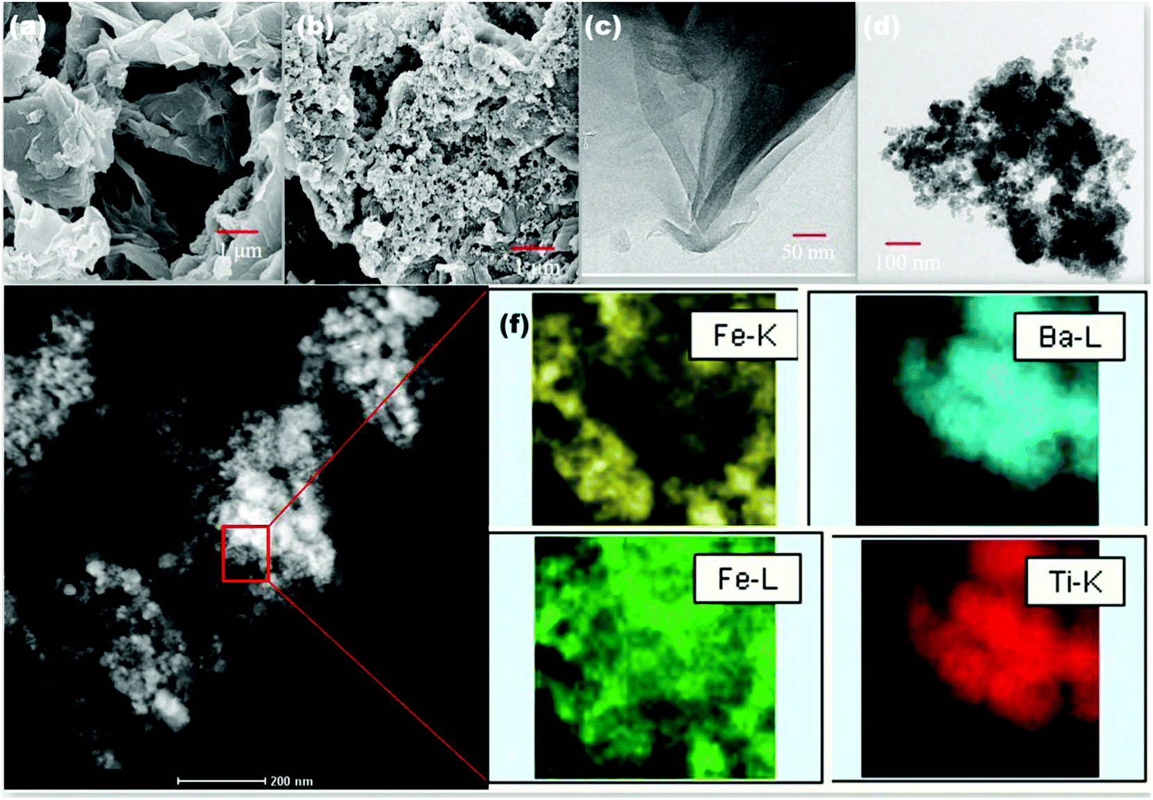
The successful synthesis of MDA modified BT/Fe co-doped GO sheets was evaluated using SEM and TEM images (Fig. 2a–d). GO shows a planar sheet like morphological structure before undergoing any modification whereas after modification a coarse morphology was obtained as inferred from SEM micrographs. Generally the coarse morphology appears to be due to the attachment of different nanoparticles on to the surfaces of the GO sheets. Similar morphological features were observed in TEM images as well. The corresponding elemental mapping analysis of MDA modified BT/Fe co-doped GO sheets suggest that the elemental distribution of Fe, Ba and Ti atoms across the GO sheets is not uniform (Fig. 2e and f). This observation clearly demonstrates the success of the step-by-step attachment process of different nanoparticles at different active sites on the GO sheets as represented in Scheme 2. Further EDS analysis shows a complete map of the BT/Fe co-doped GO sheets (Fig. S3, ESI†).
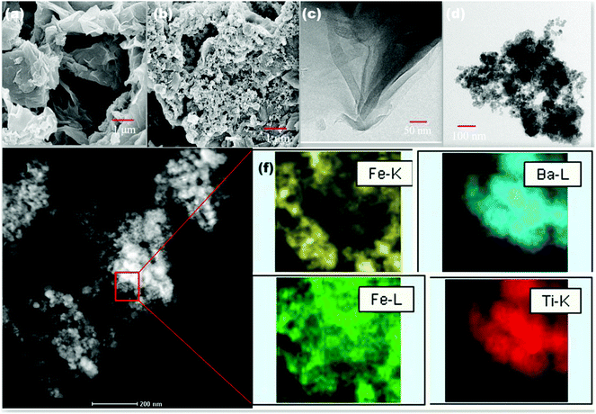 |
| | Fig. 2 SEM images of (a) GO and (b) MDA modified BT/Fe co-doped GO. TEM images of (c) GO and (d) MDA modified BT/Fe co-doped GO. (e) HAADF image of MDA modified BT/Fe co-doped GO. (f) Elemental mapping of Fe, Ba and Ti on GO sheets. | |
TGA analysis confirms that the concentration of co-doping BT/Fe is nearly 65% (Fig. 3a). FT-IR spectra also confirm the presence of BT and Fe on the GO sheets (Fig. 3b). The absorption peaks of GO corresponding to the stretching frequencies of hydroxyl (OH), carboxyl (C![[double bond, length as m-dash]](https://www.rsc.org/images/entities/char_e001.gif) O), aromatic (CC), carboxy (C–O), alcoxy (C–O) and epoxy (C–O–C) groups at wavenumbers of 3336, 1727, 1620, 1385, 1224 and 1080 cm−1 respectively are well discerned from the spectra. The disappearance of the major peaks corresponding to O-containing functional groups in MDA modified BT/Fe co-doped GO sheet samples confirmed the reduction of GO, while the presence (albeit with reduced intensity) of an N–H bending peak at 1552 cm−1 accounted for the largely intact chemically linked GO-MDA network. Additionally, the intensity of the carboxyl and epoxy peaks noticeably decreased, with the carbonyl peak of –COOH shifting to a lower wavenumber of 1719 cm−1. A new peak at 1550 cm−1 was observed, implying the presence of amine –NH in the MDA linked GO network. The disappearance of the –OH peak and existence of –NH confirmed the possible condensation of the –NH2 groups of MDA monomers with –OH and/or an epoxy opening nucleophilic addition reaction between –NH2 and epoxy groups on the basal plane. Furthermore we have analysed the modification process by Raman spectroscopy, which is a powerful tool for analysing graphitic and doped graphene oxide systems (Fig. 3c). The shifting of the D and G bands in the GO and MDA modified BT/Fe co-doped GO network provide information in terms of the intercalation and subsequent anchoring of the metal nanoparticles. The ID/IG ratio increases with the extent of GO reduction (GO (0.92) < MDA modified BT/Fe co-doped GO sheets (1.01)). This is expected as the magnitude of the ID/IG ratio is proportional to the extent of GO reduction and decreases with the number of defect domains. However, MDA modified BT/Fe co-doped GO sheets retain the characteristic features of GO, showing both the D and G-bands, albeit with reduced intensity. The X-ray diffraction patterns of the unmodified GO and MDA modified BT/Fe co-doped GO sheets are shown in Fig. 3d. The characteristic (001) and (100) diffraction peaks confirm the presence of GO. The broad (002) peak for MDA modified BT/Fe co-doped GO sheets signifies the removal of functional groups from GO and formation of reduced GO. The appearance of other characteristic peaks confirms the presence of Fe3O4 (JCPDS card no. 00-001-1111) and BaTiO3 (JCPDS card no. 00-003-0725) on the GO sheets. EMI shielding by absorption is the more preferred way of screening unwanted interference. As we have discussed earlier, EM radiation is the proliferation of both electric and magnetic components, so for significant absorption of the radiation by the shield, the shield should have electric and/or magnetic dipoles which interact with the electromagnetic fields in the incident radiation. Therefore the magnetic characterization of the synthesized material is important for designing the proper shield material. Here the magnetic performance of MDA modified BT/Fe co-doped GO nanoparticles was measured in a room temperature VSM study as shown in Fig. 3e, while the other nanomaterials used here are nonmagnetic in nature. The saturation magnetization of MDA modified BT/Fe co-doped GO nanoparticles is ca. 21 emu g−1 as observed here. It is also well known that the initial permeability is directly related to the saturation magnetization value as explained in the equation that follows:43,44
O), aromatic (CC), carboxy (C–O), alcoxy (C–O) and epoxy (C–O–C) groups at wavenumbers of 3336, 1727, 1620, 1385, 1224 and 1080 cm−1 respectively are well discerned from the spectra. The disappearance of the major peaks corresponding to O-containing functional groups in MDA modified BT/Fe co-doped GO sheet samples confirmed the reduction of GO, while the presence (albeit with reduced intensity) of an N–H bending peak at 1552 cm−1 accounted for the largely intact chemically linked GO-MDA network. Additionally, the intensity of the carboxyl and epoxy peaks noticeably decreased, with the carbonyl peak of –COOH shifting to a lower wavenumber of 1719 cm−1. A new peak at 1550 cm−1 was observed, implying the presence of amine –NH in the MDA linked GO network. The disappearance of the –OH peak and existence of –NH confirmed the possible condensation of the –NH2 groups of MDA monomers with –OH and/or an epoxy opening nucleophilic addition reaction between –NH2 and epoxy groups on the basal plane. Furthermore we have analysed the modification process by Raman spectroscopy, which is a powerful tool for analysing graphitic and doped graphene oxide systems (Fig. 3c). The shifting of the D and G bands in the GO and MDA modified BT/Fe co-doped GO network provide information in terms of the intercalation and subsequent anchoring of the metal nanoparticles. The ID/IG ratio increases with the extent of GO reduction (GO (0.92) < MDA modified BT/Fe co-doped GO sheets (1.01)). This is expected as the magnitude of the ID/IG ratio is proportional to the extent of GO reduction and decreases with the number of defect domains. However, MDA modified BT/Fe co-doped GO sheets retain the characteristic features of GO, showing both the D and G-bands, albeit with reduced intensity. The X-ray diffraction patterns of the unmodified GO and MDA modified BT/Fe co-doped GO sheets are shown in Fig. 3d. The characteristic (001) and (100) diffraction peaks confirm the presence of GO. The broad (002) peak for MDA modified BT/Fe co-doped GO sheets signifies the removal of functional groups from GO and formation of reduced GO. The appearance of other characteristic peaks confirms the presence of Fe3O4 (JCPDS card no. 00-001-1111) and BaTiO3 (JCPDS card no. 00-003-0725) on the GO sheets. EMI shielding by absorption is the more preferred way of screening unwanted interference. As we have discussed earlier, EM radiation is the proliferation of both electric and magnetic components, so for significant absorption of the radiation by the shield, the shield should have electric and/or magnetic dipoles which interact with the electromagnetic fields in the incident radiation. Therefore the magnetic characterization of the synthesized material is important for designing the proper shield material. Here the magnetic performance of MDA modified BT/Fe co-doped GO nanoparticles was measured in a room temperature VSM study as shown in Fig. 3e, while the other nanomaterials used here are nonmagnetic in nature. The saturation magnetization of MDA modified BT/Fe co-doped GO nanoparticles is ca. 21 emu g−1 as observed here. It is also well known that the initial permeability is directly related to the saturation magnetization value as explained in the equation that follows:43,44
where, constants
a and
b are determined by the material composition, magneto restriction constant is
λ, elastic strain parameter of the crystal is
ξ and
K is the proportionality coefficient. The literature also shows that in order to improve the EM absorption properties, the initial permeability of the shield should be as high as possible. So by the incorporation of these magnetic materials into the blend, which are favourable for enhancing the blend permeability, we can tune the EM absorption properties.
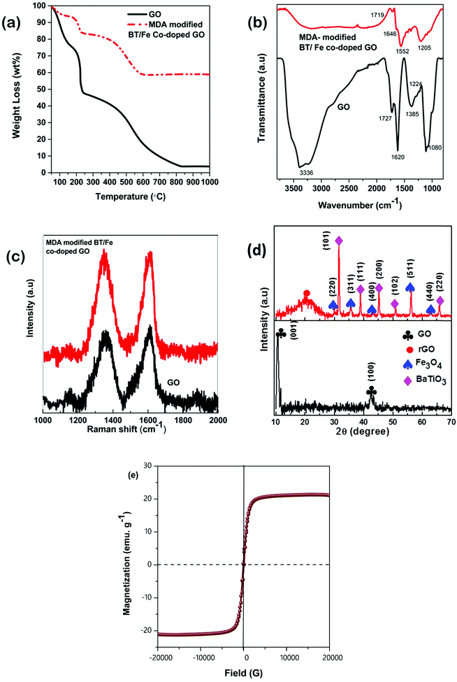 |
| | Fig. 3 (a) TGA analysis in air, (b) FT-IR spectra, (c) Raman spectra and (d) XRD analysis of GO and MDA modified BT/Fe co-doped GO. (e) Magnetization of MDA modified BT/Fe co-doped GO. | |
Component specific dispersion of functional nanoparticles
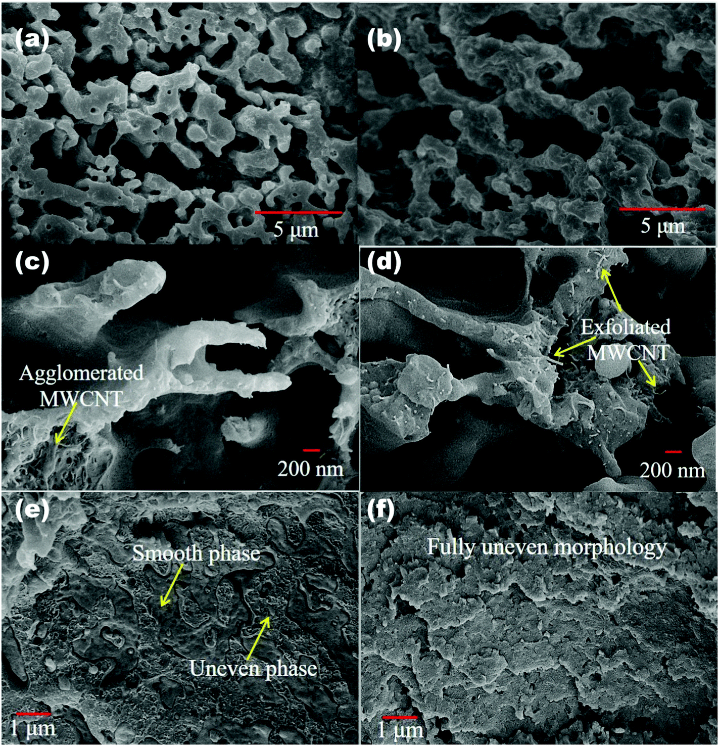
The lack of specific interactions between two immiscible polymer components generally leads to the formation of a heterogeneous morphology. From SEM micrographs we observe a co-continuous type of morphology in 50/50 blends of PC/PVDF (Fig. 4a). It is also observed that after the addition of nanoparticles, the overall blend morphology is still co-continuous in nature (Fig. 4b). An SEM micrograph at higher magnification clearly shows the preferential localization of the conducting nanoparticles (MWCNTs) in the PVDF as the other component (PC) was already etched out for better clarity (Fig. 4c and d). Furthermore, it was also observed that exfoliation of the conducting MWCNTs has improved significantly after surface modification with ACA molecules, as manifested from the better interconnected network of nanotubes inside a given component. The DSC study also suggests that MWCNTs are localized primarily in the PVDF component influencing the crystallization temperature of the PVDF significantly (Fig. S4, ESI†). It is further observed that MDA modified BT/Fe co-doped GO was also specifically localized in the PVDF resulting in a coarser morphology as observed from SEM. On the other hand, the PC component appeared smooth which begins to suggest that the particles are only localized in the PVDF (Fig. 4e). From our previous study it is observed that though PC is thermodynamically favourable, the nanoparticles still prefer PVDF due to its higher polarity as compared to PC.45,46 However, tailor-made localization of the nanoparticles in the different components can be accomplished by preparing PC nanocomposites and by adopting the sequential mixing protocol which we have discussed earlier. As a result the overall morphology appeared much finer as observed from an SEM micrograph (Fig. 4f).
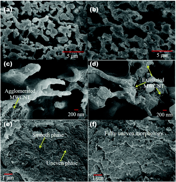 |
| | Fig. 4 SEM micrograph of (a) 50/50 neat PC/PVDF blend, (b) PC/PVDF with MWCNT-ACA + MDA modified r-GO/BT/Fe (PC phase etch out in both cases for better resolution). High resolution SEM micrograph of (c) PC/PVDF with MWCNT, (d) PC/PVDF with MWCNT-ACA (arrows indicate the position of MWCNTs) (PC phase etch out in both cases for better resolution). SEM micro graph of (e) PC/PVDF with MWCNT-ACA + MDA modified r-GO/BT/Fe, (f) PC/PVDF with MWCNT-ACA + MDA modified r-GO/BT/Fe (in PC phase). | |
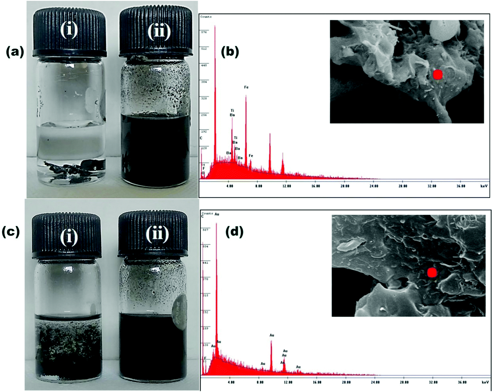
Interestingly, the tailor-made localization of different nanoparticles in the different components was analysed more accurately by selective dissolution testing and EDS. For PC/PVDF containing both MWCNT-ACA and MDA modified BT/Fe co-doped GO, the selective dissolution of the components in their respective solutions further confirms that all the nanoparticles are in the PVDF phase. This is observed from the black color of the extract of PVDF, whereas the extraction of PC yields a colorless solution (Fig. 5a). The corresponding EDS analysis, where PC is completely etched out, shows the presence of Ba, Ti, and Fe in the PVDF phase (Fig. 5b). Now, for the sample where a sequential mixing protocol was adopted a black colored solution was obtained by dissolving the PC, which confirms the localization of the BT/Fe co-doped GO in the PC (Fig. 5c). Furthermore, EDS spectra of the PC etched samples confirm no migration of the MDA modified BT/Fe co-doped GO into the PVDF phase (Fig. 5d).
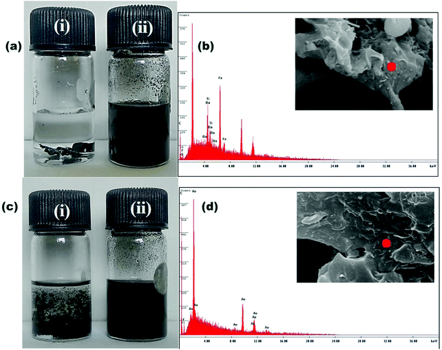 |
| | Fig. 5 (a) Solution dissolution test of a sample of PC/PVDF with MWCNT-ACA + MDA modified r-GO/BT/Fe: (i) the colorless PC extract confirms that particles are not localized in the PC phase, whereas (ii) the black colored PVDF extract confirms that all the particles are localized in the PVDF phase. (b) EDS experiment on a cryofractured PC etched sample confirms that all the particles are in the PVDF phase. (c) Solution dissolution test of a sample of PC/PVDF with MWCNT-ACA + MDA modified BT/Fe co-doped GO: (i) the slightly black colored PC extract and (ii) black colored PVDF extract both confirm that particles are in both phases. (d) EDS experiment on a cryofractured PC etched sample confirms no migration of BT and Fe into the PVDF phase after selectively localizing them in the PC phase. | |
It is well established that the addition of nanoparticles results in enhancement of the functional properties in immiscible blend structures, however, localizing them in a specific component further results in intriguing properties like high electrical conductivity, and improved structural and other functional properties. The effect of localizing different nanoparticles in different components was further investigated with respect to their mechanical behavior (Fig. S5, ESI†). Interfacial adhesion between the constituents is the prime factor that decides the mechanical properties of the blend system. Furthermore it also observed that the overall mechanical properties were greatly influenced by the localization of the different nanoparticles. Poor stress transfer at the interface results in catastrophic failure when both the nanoparticles are in the PVDF, while the tensile strength and Young's modulus are relatively enhanced. However localizing the different nanoparticles in different components results in an overall improvement in the mechanical properties.
Charge transport in the blends: the effect of localizing functional nanoparticles in specific components
It is imperative to note that the primary mechanism of the shielding is attributable to the reflection of the incident EM wave from the surface of the shield. Mobile charge carriers or an interconnected conducting network inside the shield play an important role in such characteristics. However later studies have explained that the interaction of the incident EM radiation with the conducting path of the shield is preferred over higher electrical conductivity. The strategic dispersion of various conducting nanomaterials inside an immiscible polymer blend generates the desired interconnected network of conducting particles that is required for shielding.47,48 The preferential localization of conducting MWCNTs in an energetically preferred component (PVDF here) readily enhances the blend conductivity due to double percolation phenomena. Interestingly, here we observe that the modification of the MWCNTs with ACA enhances the overall blend conductivity (Fig. 6). The agglomeration of MWCNTs, driven by van der Waals' forces of attraction, can easily be overcome by such non-covalent modification strategies without disturbing the structural integrity of the MWCNTs. The volume conductivity of the blends was fitted using a power law model, which is a useful tool to understand the contribution of network formation to the charge transportation mechanism. The decrease in the exponent value clearly indicates the effective dispersion that significantly facilitates effective charge transport through hopping, while previously it was by tunnelling (Table T1, ESI†). However the preferential localization of a second nanomaterial into the same component often impedes the interconnected network, thereby reducing the overall blend conductivity. In light of this, we have adopted a unique strategy wherein the conducting and the magnetic phases are localized in different components of the blend following a sequential mixing protocol. A nucleophilic substitution reaction governs the localization of the MDA modified BT/Fe co-doped GO nanoparticles in the PC, whereas the MWCNTs are preferentially localised in the PVDF. Such a strategy is essential to retain the three dimensional networks which are formed by the individual fillers in their specific component of the blend. Moreover the charge transportation phenomenon is also unaltered inside the blend by this unique arrangement.
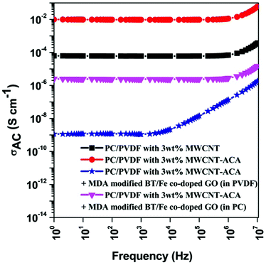 |
| | Fig. 6 AC electrical conductivity of various blends. | |
EMI shielding properties of individual layers
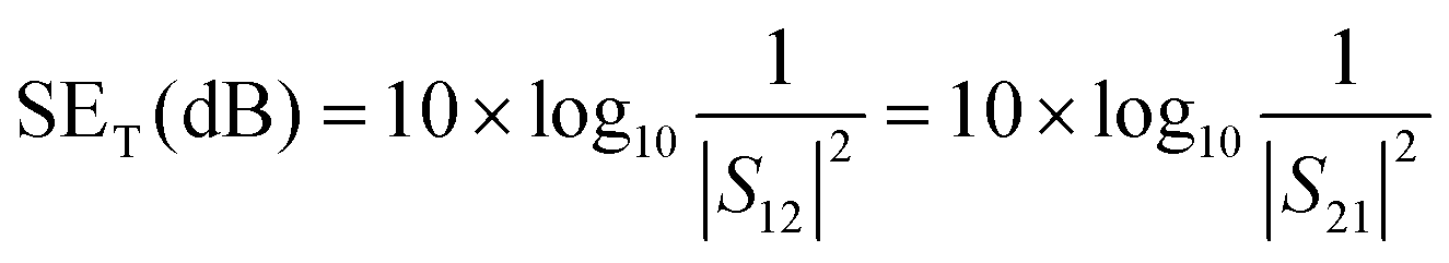
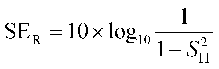
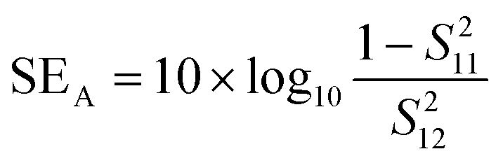
The amount of incident EM attenuation is analysed here through a total shielding effectiveness (SET) in the X and Ku frequency bands, which is expressed in dB. It is a quantitative measure of the blocking of EM waves by the shield materials. EM attenuation occurs due to the interaction of incident EM waves with the shielding materials through a combination of three different major mechanisms, whereas the remaining waves are transmitted. Shielding by reflection (SER) is one of the primary EM attenuation mechanisms, and occurs due to the impedance mismatch between the air and the shield material, whereas shielding by absorption (SEA) is the other mechanism, which mainly functions to dissipate EM radiation energy into heat. The other mechanism is shielding by multiple reflection (SEMR), which occurs due to successive reflection between two different walls inside the matrix. In contrast, the contribution of SEMR is negligible when the shielding by absorption is greater than 10 dB, where most of the reflected wave will be absorbed within the shield.49 In this context SET can be expressed as,Mathematically the total shielding effectiveness can be estimated by this equation as follows;| | | SET = 10log(Pt/Pi) | (3) |
where Pi and Pt are the powers of the incident and transmitted electric field intensities respectively. However here we estimated the total shielding effectiveness by using scattering parameters which were obtained from a vector network analyzer (VNA).| |  | (4) |
where S12 is a reverse transmission coefficient whereas S21 is a forward transmission coefficient. We can also access the total reflection and absorption components from the measured scattering parameters using the following equations,| |  | (5) |
| |  | (6) |
where S11 is a forward reflection coefficient.
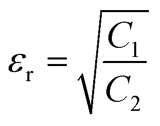
Fig. 7a depicts the frequency dependent total shielding efficiencies of various blends. Considerable shielding efficiency is observed with the addition of MWCNTs while neat blends are transparent to EM radiation. As we have discussed earlier, the preferential localization of MWCNTs into the energetically favoured phase of an immiscible polymer blend leads to a significant enhancement in the AC electrical conductivity that is observed through the formation of interconnected conducting networks. So, the material should have adequate electrical conductivity for interacting with the EM radiation. A significant improvement in SET is observed (see Table T2, ESI†) upon increasing the content of MWCNTs which ensures the formation of a finer mesh structure for facilitating the charge transport. Additionally, because of its large specific surface area, a finer mesh like structure can also assist in multiple scattering inside the network which may contribute to higher shielding efficiency. Better exfoliation of the conducting nanoparticles (ACA modified MWCNTs) results in further enhancement of the shielding efficiency when compared with unmodified MWCNTs. However after the addition of MDA modified BT/Fe co-doped GO nanoparticles into the blend, the mechanism of the shielding efficiency was completely changed. Interestingly the localization of MDA modified BT/Fe co-doped GO nanoparticles also has a significant effect on the total shielding efficiency. Better shielding efficiency is observed after the addition of MDA modified BT/Fe co-doped GO nanoparticles in PC which generates two distinct microphases inside the blend structure. The local field variation of the different dielectric constant materials readily absorbs the incident EM radiation by dissipating the energy into heat.13 To assess the mechanism of shielding, we compared the complex (relative) permittivities (εr) and the complex relative permeabilities (μr) of the blends through well-established line theory.50 The complex parameters can also be expressed as  and
and  . Where
  and
and  , where Z is the impedance of the specimen and Γ is the reflection coefficient in an air filed coaxial line. As we used VNA for characterize the shielding properties of the blends, the scattering parameters obtained from VNA can be expressed as,46
 |
| | Fig. 7 (a) Total shielding effectiveness, (b) total loss parameters, (c) attenuation constants, and (d) total absorptions of various samples. | |
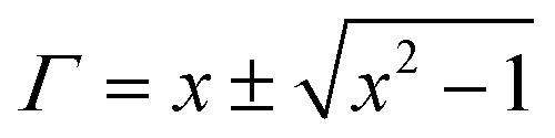
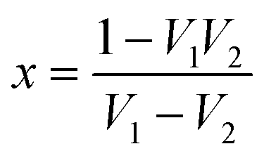
Now by using the scattering parameters the reflection coefficient can be calculated by the following equation,
| |  | (9) |
where,

.
In general the complex permittivity and permeability parameters convey the ability of a material to attenuate EM radiation by absorption, whereas the storage ability is the main source of polarization and the dissipated energy is associated with the loss.51
From the scattering parameter expression it also observed that these complex parameters are directly related to the absorption and reflection coefficients of the total shielding efficiency as follows:7
| |  | (10) |
| |  | (11) |
where
μ =
μ0μr and
σ = 2π
fε0ε′′. So it is clear that shielding by absorption is increased with increasing values of
μr and
εr where
μr =
μ′ −
jμ′′ and
εr =
ε′ −
jε′′. The complex permittivity and permeability parameters are frequency dependent and the real parts mainly represent the storage ability whereas the imaginary parts correspond to the loss.
52–54 The dielectric loss is primarily attributed to conductivity and polarization loss. The polarization loss can further be resolved into ionic polarization, electronic polarization, dipole orientation polarization and interfacial polarization.
55 Here the conductivity loss mainly arises due to charge transportation by the MWCNT network and the polarization loss originates from interfacial polarization due to the effect of the heterogeneous dielectric medium. Ionic and electronic polarization can be excluded as they are generated in the infrared region. The energy consumption is also negligible in terms of dielectric orientation polarization. So we can conclude that the dielectric losses arise mainly due to the interfacial polarization and conductivity losses. The magnetic permeability is attributed to the BT/Fe co-doped GO nanoparticle incorporation into the blend. A high initial permeability also predicts high magnetic loss in the materials.
55 An increased
Ms is generally favourable for a higher initial permeability. However, lossy materials like BT (in the microwave regime) also enhance the dielectric losses, whereas the magnetic permeability is due to the incorporation of ferrimagnetic doping onto the GO sheets. Fig. S6 (ESI
†) clearly depicts the real and imaginary parts of the permittivity and permeability parameters. Interestingly it is observed that the preferential localization of the nanoparticles also influences the permittivity and permeability values. As the dissipated energy is associated with the loss parameters, here we evaluated the consolidated loss parameters by evaluating the dielectric tangent loss (tan
δε =
ε′′
/ε′) and magnetic tangent loss (tan
δμ =
μ′′/
μ′). The energy loss in a material irradiated by electromagnetic waves comes about through damping forces acting on polarized atoms and molecules and through the finite conductivity of a material. According to the Poynting theorem, the total power of a harmonic electromagnetic field with a sufficient angular frequency entering a volume through the surface goes partially into increasing the field energy stored inside the volume and partially is lost as heat.
56 It is also observed that the conductive and dielectric losses are indistinguishable with respect to heat generation.
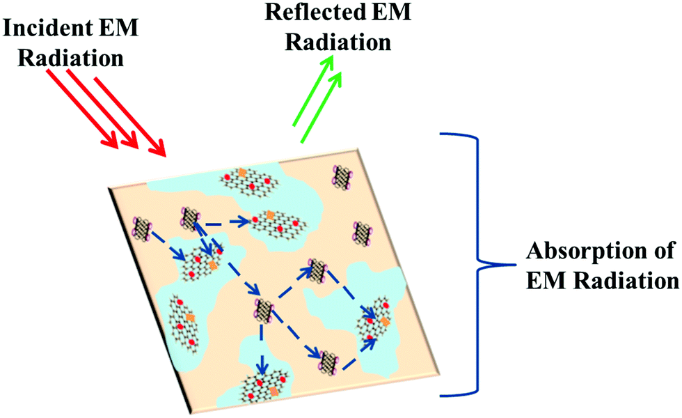
57 So, when an external electromagnetic field encounters the designed material, the material guides the EM waves to cross the variety of microscopic boundaries that constitute the heterostructure. Furthermore, subsequent local field variations can have considerable effects on the absorption of energies at such heterogeneous boundaries because the absorption depends quadratically upon the electric field intensity.
13 Due to Maxwell–Wagner–Sillars polarization, virtual charges are accumulated at the interface of two different materials and the whole of the energy is dissipated through Joule heating.
13 Furthermore, the obtained heat is easily dissipated through the conducting network of MWCNTs. It is observed from
Fig. 7b that the consolidated loss parameters are further improved by the addition of magnetic nanoparticles into the blend. This is because magnetic loss originates from the magnetic hysteresis losses due to natural resonances and eddy currents at GHz frequencies. However the generation of two distinct microstructures with two different dielectric materials leads to the polarization of the virtual charges followed by Maxwell–Wagner–Sillars polarization, further enhancing the loss parameters. The attenuation constant, which is the EM absorption ability, can also be evaluated by the corresponding permittivity and permeability parameters. The attenuation constant can express as follows:
58| |  | (12) |
where
c is the speed of light. So it is important, in order to satisfy the desire for higher attenuation ability materials, that the magnetic and dielectric losses be as high as possible.
Fig. 7c shows that the attenuation constant is increased significantly after the addition of magnetic nanoparticles into the blend, whereas it is also modified further after the selective localization of the magnetic nanoparticles into the PC phase. The large difference in the real and imaginary permittivity or permeability parameters
versus other blend materials is the main reason behind this, which is clearly observed from the tangent loss parameters’ values. Therefore, it can be concluded that a synergistic effect
59–61 from both the magnetic and dielectric phases together with the conducting phase played a pivotal role in this material exhibiting very high EM attenuation driven by absorption (
Fig. 7d and Fig. S7, ESI
†). The magneto-dielectric behavior of the BT/Fe co-doped GO nanoparticles was analysed by magneto-capacitance measurements, by varying the magnetic field from 0 to 10
000 Oe (Fig. S8, ESI
†). It is evident that the designed materials clearly show magnetoelectric coupling. It is envisaged that materials can exhibit a magnetic-field-dependent dielectric response without any magnetism. Our nanocomposites showed a magneto-capacitance (MC) effect with the MC changing by 10% as the magnetic field was increased to 1 T. This effect was explained as arising because of Maxwell–Wagner polarization as applied to inhomogeneous materials.
Fig. S9 (ESI†) clearly exhibits the synergistic effect of both complex parameters in an EM shielding application. This extensive study of the permittivity and permeability parameters explains the change in the shielding mechanism after the incorporation of BT/Fe GO nanoparticles in the PC component and MWCNT-ACA in the PVDF component. We have schematically illustrated the shielding mechanism (see Scheme 4) for the sample with the highest attenuation. Furthermore by reducing the surface conductivity of the samples we can reduce the surface reflections and hence most of the incident radiation penetrates into the shield and gets absorbed when it encounters the hybrid materials. Generally, impedance mismatch is the key factor for surface reflection of an incident EM wave. To achieve zero reflection, the characteristic impedance of the shield should be equal/close to that of the free space.38,62 The characteristic impedance is always determined by the relationship between the real parts of the complex permittivity and permeability parameters. If the real part of the complex permittivity is much higher than the real part of the complex permeability, most of the incident electromagnetic waves will be reflected off the surface due to low surface resistance, rather than penetrating into the shield. Therefore, we have estimated the ratios of the real parts of the permittivity and permeability parameters which should be close to 1 for better impedance matching. Fig. S10 (ESI†) shows that an MWCNT-ACA containing blend showed a higher ratio and thus its effective microwave absorption will be hindered by the poorly matched intrinsic characteristic impedance. Conversely, when hybrid nanomaterials are present in the blend, the gap between the two real parts of the complex parameters is narrowed, which leads to good impedance matching, thereby enhancing the absorption efficiency. EM shielding for individual particles like BT or Fe nanoparticles has been reported, however, our study demonstrates synergistic effects when both dielectric (BT) and magnetic (Fe) phases are co-doped on GO sheets. This study also suggests that the precise localization of different nanoparticles in an immiscible polymer blend also helps the EM shielding efficiency.
 |
| | Scheme 4 EM shielding mechanism for PC/PVDF blends with 3 wt% MWCNT-ACA + MDA modified BT/Fe GO in PC. | |
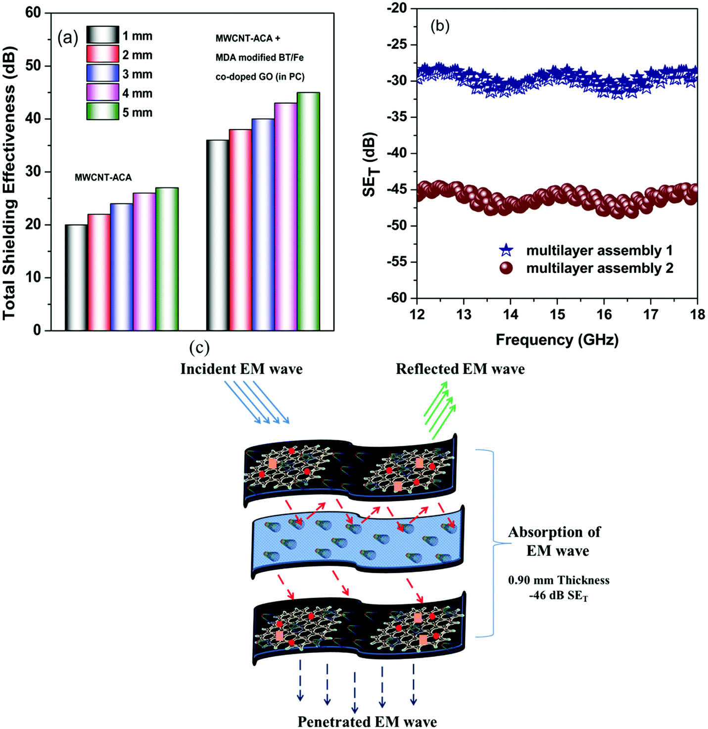
Fabrication of a multilayer structure for high performance screening
The thickness of the shielding material is an important parameter for its applications.7 In general, EM attenuation can be correlated to the skin depth of the individual material and scales up with the thickness. The skin depth is the intensity of penetration into the conductive material at which generally electric field drops to 1/e, which roughly measures absorption efficiency of the screening material. It is shown that the skin depth readily decreased from 4.8 mm (when only MWCNT-ACA was present) to 1.5 mm after incorporating BT/Fe co-doped GO nanoparticles along with MWCNT-ACA in two different phases, indicating a boost in the EM attenuation (see Fig. 8a). If we enhance the shield thickness, SET does not change any more after the critical skin depth has been reached. The main goal is an ultra-thin shield material, for a new generation of applications. The promising shielding performance of the individual materials with different shielding mechanisms encouraged us to design a multilayer assembly of various polymer nanocomposites which provides a better ability to attenuate EM radiation than the individual materials.63,64 It is observed from the previous section that the incorporation of hybrid nanomaterials into the matrix can enhance the overall shielding efficiency by absorbing the incident EM radiation, whereas a blend with only conductive nanomaterials is prone to reflect back the incident EM radiation from the surface of the shield material. By designing the outer layers with nanocomposites containing PVDF with 3 wt% MWCNT-ACA, and by designing the inner layers with PC/PVDF with 3 wt% MWCNT-ACA + MDA modified BT/Fe co-doped GO (in PC), we can suppress EM radiation significantly. This arrangement (multilayer assembly 1 in Fig. 8a) provides us with a shielding of −30 dB, whereas modulating the inner layers with PVDF with 3 wt% MWCNT-ACA and outer layers with PC/PVDF with 3 wt% MWCNT-ACA + MDA modified BT/Fe co-doped GO (in PC) provides us with an even better shielding efficiency of −46 dB (multilayer assembly 2 in Fig. 8a). So it is observed that we can tune the total shielding effectiveness of the multilayer assembly by rational arrangement of the layers. The motivation behind arranging PC/PVDF with 3 wt% MWCNT-ACA + MDA modified BT/Fe co-doped GO (in PC) in the outer layers is to maximize the penetration of incoming EM radiation due to better impedance matching, whereas blends of only conducting materials reflect back the incident EM radiation due to surface scattering. However, most of the penetrating radiation encounters the heterogeneous dielectric medium which was constructed using MWCNT-ACA (in PVDF) and MDA modified BT/Fe co-doped GO (in PC). As we discussed earlier, the microscopic boundaries of the heterostructure can readily absorb any external electromagnetic field and dissipate it into heat. Therefore, most of the penetrating radiation can readily be absorbed at the outer layer of the multilayer assembly. The residual penetrating radiation then encounters the inner layer of the assembly which is conducting. The role of the conducting surface is to reflect back most of the incident wave which is eventually scavenged by the outer layers. The penetrating waves can undergo multiple reflections within the inner layer. Finally the presence of a heterostructure in the outer layer can absorb the remaining fraction of the radiation. Moreover, the accumulation of virtual charges at the interface of the two layers, having different dielectric constants and conductivities, leads to interfacial polarization, which will also enhance the total EM shielding efficiency. Taken together, our study clearly demonstrates that by two different mechanisms of shielding the overall shielding can be improved many fold through multilayer assembly, as compared to the individual layers. The addition of BT/Fe co-doped GO sheets helps in retaining the charge transport through the conducting network of MWCNTs besides causing dielectric loss. These, along with the MWCNTs, act as nano-capacitors in the individual components. A schematic representation of the EM attenuation mechanism is explained in the Fig. 8b. The EM shielding properties of various PVDF or PC based composites and blends with different nanomaterials are shown in Table T3 (ESI†).
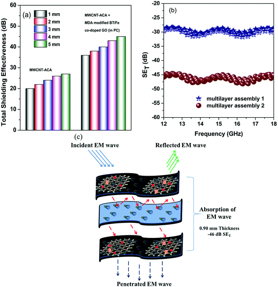 |
| | Fig. 8 (a) Total shielding effectiveness with different thicknesses, (b) the total shielding effectiveness of the designed multilayer assembly and (c) the shielding mechanism of assembly 2. | |
Conclusion
In summary, we have demonstrated that the strategic dispersion of conducting and highly lossy magnetic nanomaterials in two different phases of an immiscible polymer blend system can systematically enhance the bulk electrical conductivity and EM shielding properties. The exfoliation of the conducting phase is successfully enhanced through the non-covalent attachment of an anthracene derivative on the surface of the MWCNTs, and by restricting it to PVDF enhanced volume electrical conductivity was achieved. Furthermore, restricting the BT/Fe co-doped GO to the PC phase helps in retaining its bulk electrical conductivity and excellent shielding ability. The successful synthesis of hybrid lossy nanomaterials through a step-by-step reduction process of GO sheets with BT, MDA and Fe3O4 nanoparticles results in synergistic shielding. The individual layers showed an exceptional SE of −35 dB at 18 GHz (dominated by absorption, 85%) which was further enhanced to −46 dB by the rational arrangement of thin layers. This study will not only bolster research in multifaceted applications toward cost-effective solutions to modern electronic interfaces, but also promote a quantitative understanding of structure–property correlations towards the nanofabrication of graphene-based multifunctional materials. Further multilayer assembly of a rational arrangement of different individual layers results in outstanding shielding performance with a thickness of only 0.90 mm, suggesting new pathways for designing modern light weight shielding materials.
Competing financial interest
The authors declare no competing financial interests.
Acknowledgements
We sincerely acknowledge Ms Dipanwita Chatterjee (Materials Research Centre, IISc Bangalore) for helping us with the TEM studies and Dr Amit Kumar (Materials Engineering, IISc Bangalore) for helping us in the magneto-dielectric study. The authors gratefully acknowledge financial support from the Science & Engineering Research Board, DST (India).
References
- Y. Yang, M. C. Gupta, K. L. Dudley and R. W. Lawrence, Nano Lett., 2005, 5, 2131–2134 CrossRef CAS PubMed.
- S. Dhawan, N. Singh and D. Rodrigues, Sci. Technol. Adv. Mater., 2003, 4, 105–113 CrossRef CAS.
-
S. Celozzi, G. Lovat and R. Araneo, Electromagnetic shielding, Wiley Online Library, 2008 Search PubMed.
- D. Chung, Carbon, 2001, 39, 279–285 CrossRef CAS.
- L. Li, P. Zhao, Y. Luo, H. Yu, J. Tao, D. He, W. Gong, D. Li, Z. Wang and Z. Peng, RSC Adv., 2017, 7, 1093–1100 RSC.
- M. González, M. Crespo, J. Baselga and J. Pozuelo, Nanoscale, 2016, 8, 10724–10730 RSC.
- M. H. Al-Saleh and U. Sundararaj, Carbon, 2009, 47, 1738–1746 CrossRef CAS.
- Y. Wang and X. Jing, Polym. Adv. Technol., 2005, 16, 344–351 CrossRef CAS.
- H.-B. Zhang, Q. Yan, W.-G. Zheng, Z. He and Z.-Z. Yu, ACS Appl. Mater. Interfaces, 2011, 3, 918–924 CAS.
- S. P. Pawar, S. Biswas, G. P. Kar and S. Bose, Polymer, 2016, 84, 398–419 CrossRef CAS.
- S. Geetha, K. Satheesh Kumar, C. R. Rao, M. Vijayan and D. Trivedi, J. Appl. Polym. Sci., 2009, 112, 2073–2086 CrossRef CAS.
- S. R. Dhakate, K. M. Subhedar and B. P. Singh, RSC Adv., 2015, 5, 43036–43057 RSC.
- F. Qin and C. Brosseau, J. Appl. Phys., 2012, 111, 061301 CrossRef.
- S. Biswas, G. P. Kar and S. Bose, ChemNanoMat, 2016, 2, 140–148 CrossRef CAS.
- N. Li, Y. Huang, F. Du, X. He, X. Lin, H. Gao, Y. Ma, F. Li, Y. Chen and P. C. Eklund, Nano Lett., 2006, 6, 1141–1145 CrossRef CAS PubMed.
- Z. Liu, G. Bai, Y. Huang, Y. Ma, F. Du, F. Li, T. Guo and Y. Chen, Carbon, 2007, 45, 821–827 CrossRef CAS.
- R. Ramasubramaniam, J. Chen and H. Liu, Appl. Phys. Lett., 2003, 83, 2928–2930 CrossRef CAS.
- M. H. Al-Saleh, W. H. Saadeh and U. Sundararaj, Carbon, 2013, 60, 146–156 CrossRef CAS.
- S. Pande, A. Chaudhary, D. Patel, B. P. Singh and R. B. Mathur, RSC Adv., 2014, 4, 13839–13849 RSC.
- D. Ponnamma, K. K. Sadasivuni, Y. Grohens, Q. Guo and S. Thomas, J. Mater. Chem. C, 2014, 2, 8446–8485 RSC.
- T. Kuilla, S. Bhadra, D. Yao, N. H. Kim, S. Bose and J. H. Lee, Prog. Polym. Sci., 2010, 35, 1350–1375 CrossRef CAS.
- Z. Chen, C. Xu, C. Ma, W. Ren and H. M. Cheng, Adv. Mater., 2013, 25, 1296–1300 CrossRef CAS PubMed.
- J. Liang, Y. Wang, Y. Huang, Y. Ma, Z. Liu, J. Cai, C. Zhang, H. Gao and Y. Chen, Carbon, 2009, 47, 922–925 CrossRef CAS.
- M.-S. Cao, X.-X. Wang, W.-Q. Cao and J. Yuan, J. Mater. Chem. C, 2015, 3, 6589–6599 RSC.
- Y.-J. Wan, S.-H. Yu, W.-H. Yang, P.-L. Zhu, R. Sun, C.-P. Wong and W.-H. Liao, RSC Adv., 2016, 6, 56589–56598 RSC.
- A. Kumar and P. S. Alegaonkar, ACS Appl. Mater. Interfaces, 2015, 7, 14833–14842 CAS.
- K. Yao, J. Gong, N. Tian, Y. Lin, X. Wen, Z. Jiang, H. Na and T. Tang, RSC Adv., 2015, 5, 31910–31919 RSC.
- Z. Lu, L. Ma, J. Tan, H. Wang and X. Ding, Nanoscale, 2016, 8, 16684–16693 RSC.
- X. Jian, B. Wu, Y. Wei, S. X. Dou, X. Wang, W. He and N. Mahmood, ACS Appl. Mater. Interfaces, 2016, 8, 6101–6109 CAS.
- Y. Tang, Y. Shao, K. Yao and Y. Zhong, Nanotechnology, 2013, 25, 035704 CrossRef PubMed.
- A. P. Singh, P. Garg, F. Alam, K. Singh, R. Mathur, R. Tandon, A. Chandra and S. Dhawan, Carbon, 2012, 50, 3868–3875 CrossRef CAS.
- W.-L. Song, X.-T. Guan, L.-Z. Fan, W.-Q. Cao, C.-Y. Wang, Q.-L. Zhao and M.-S. Cao, J. Mater. Chem. A, 2015, 3, 2097–2107 CAS.
- M. Verma, A. P. Singh, P. Sambyal, B. P. Singh, S. Dhawan and V. Choudhary, Phys. Chem. Chem. Phys., 2015, 17, 1610–1618 RSC.
- D. Han, Y.-H. Zhao, S.-L. Bai and W. C. Ping, RSC Adv., 2016, 6, 92168–92174 RSC.
- S. K. Marka, B. Sindam, K. J. Raju and V. V. Srikanth, RSC Adv., 2015, 5, 36498–36506 RSC.
- Y. Yang, M. Li, Y. Wu, T. Wang, E. S. G. Choo, J. Ding, B. Zong, Z. Yang and J. Xue, Nanoscale, 2016, 8, 15989–15998 RSC.
- P. Saini, V. Choudhary, N. Vijayan and R. Kotnala, J. Phys. Chem. C, 2012, 116, 13403–13412 CAS.
- M.-S. Cao, W.-L. Song, Z.-L. Hou, B. Wen and J. Yuan, Carbon, 2010, 48, 788–796 CrossRef CAS.
- P. Saini, M. Arora, G. Gupta, B. K. Gupta, V. N. Singh and V. Choudhary, Nanoscale, 2013, 5, 4330–4336 RSC.
- A. Kumar, A. P. Singh, S. Kumari, A. K. Srivastava, S. Bathula, S. K. Dhawan, P. K. Dutta and A. Dhar, J. Mater. Chem. A, 2015, 3, 13986–13993 CAS.
- Y. Yang, M. Li, Y. Wu, T. Wang, E. S. G. Choo, J. Ding, B. Zong, Z. Yang and J. Xue, Nanoscale, 2016, 8, 15989–15998 RSC.
- G. P. Kar, S. Biswas, R. Rohini and S. Bose, J. Mater. Chem. A, 2015, 3, 7974–7985 CAS.
- R. Lv, F. Kang, J. Gu, X. Gui, J. Wei, K. Wang and D. Wu, Appl. Phys. Lett., 2008, 93, 223105 CrossRef.
- C.-L. Zhu, M.-L. Zhang, Y.-J. Qiao, G. Xiao, F. Zhang and Y.-J. Chen, J. Phys. Chem. C, 2010, 114, 16229–16235 CAS.
- S. Biswas, G. P. Kar and S. Bose, Nanoscale, 2015, 7, 11334–11351 RSC.
- S. Biswas, G. P. Kar and S. Bose, ACS Appl. Mater. Interfaces, 2015, 7, 25448–25463 CAS.
- N. F. Colaneri and L. Schacklette, IEEE Trans. Instrum. Meas., 1992, 41, 291–297 CrossRef.
- M. H. Al-Saleh and U. Sundararaj, Macromol. Mater. Eng., 2008, 293, 621–630 CrossRef CAS.
- S. Biswas, G. P. Kar and S. Bose, J. Mater. Chem. A, 2015, 3, 12413–12426 CAS.
- R. B. Schulz, V. Plantz and D. Brush, IEEE Trans. Electromagn. Compat., 1988, 30, 187–201 CrossRef.
- I. Arief, S. Biswas and S. Bose, ACS Appl. Mater. Interfaces, 2016, 8, 26285–26297 CAS.
- S. Biswas, G. P. Kar and S. Bose, Phys. Chem. Chem. Phys., 2015, 17, 27698–27712 RSC.
- G. P. Kar, S. Biswas and S. Bose, Mater. Res. Express, 2016, 3, 064002 CrossRef.
- V. Bhingardive, T. Woldu, S. Biswas, G. P. Kar, S. Thomas, N. Kalarikkal and S. Bose, ChemistrySelect, 2016, 1, 4747–4752 CrossRef CAS.
- D. Ding, Y. Wang, X. Li, R. Qiang, P. Xu, W. Chu, X. Han and Y. Du, Carbon, 2017, 111, 722–732 CrossRef CAS.
-
R. E. Collin, Foundations for microwave engineering, John Wiley & Sons, 2007 Search PubMed.
- D. Ding, Y. Wang, X. Li, R. Qiang, P. Xu, W. Chu, X. Han and Y. Du, Carbon, 2017, 111, 722–732 CrossRef CAS.
- W. Li, H. Qi, X. Niu, F. Guo, X. Chen, L. Wang and B. Lv, RSC Adv., 2016, 6, 24820–24826 RSC.
- X. Zhang, Y. Li, R. Liu, Y. Rao, H. Rong and G. Qin, ACS Appl. Mater. Interfaces, 2016, 8, 3494–3498 CAS.
- K. Chen, C. Xiang, L. Li, H. Qian, Q. Xiao and F. Xu, J. Mater. Chem., 2012, 22, 6449–6455 RSC.
- Z. Wang, L. Wu, J. Zhou, W. Cai, B. Shen and Z. Jiang, J. Phys. Chem. C, 2013, 117, 5446–5452 CAS.
- S. Kumar, G. Datt, A. S. Kumar and A. Abhyankar, J. Appl. Phys., 2016, 120, 164901 CrossRef.
- S. Biswas, S. S. Panja and S. Bose, Mater. Chem. Front., 2017, 1, 132–145 RSC.
- Y. Bhattacharjee, V. Bhingardive, S. Biswas and S. Bose, RSC Adv., 2016, 6, 112614–112619 RSC.
Footnote |
| † Electronic supplementary information (ESI) available: Preparation of PC nanocomposite, UV-Vis spectra of washed solution, EDS analysis of MDA modified BT/Fe co-doped GO nanoparticles, DSC experiments on blends, mechanical properties of blends, complex permittivity and permeability, absorption and reflection percentages, magneto-dielectric study, synergistic effect of absorption, impedance matching, table of parameters obtained from power law fitting, table of total shielding effectiveness of various shield materials with different thicknesses, and table of EM shielding performances of various PVDF and PC based matrices with MWCNTs and/or GO as filler nanoparticles. See DOI: 10.1039/c6qm00335d |
|
| This journal is © the Partner Organisations 2017 |

 *b
*b


 and
and 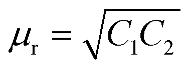 . Where
 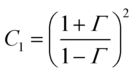 and
and 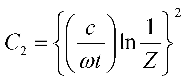 , where Z is the impedance of the specimen and Γ is the reflection coefficient in an air filed coaxial line. As we used VNA for characterize the shielding properties of the blends, the scattering parameters obtained from VNA can be expressed as,46
 .
.