Optimization of perovskite by 3D twisted diketopyrrolopyrrole for efficient perovskite solar cells†
Bin
Huang‡
a,
Qingxia
Fu‡
a,
Qingyun
Ai
a,
Licheng
Tan
ab,
Lie
Chen
*ab and
Yiwang
Chen
 *ab
*ab
aCollege of Chemistry, Nanchang University, 999 Xuefu Avenue, Nanchang 330031, China. E-mail: chenlie@ncu.edu.cn
bJiangxi Provincial Key Laboratory of New Energy Chemistry/Institute of Polymers, Nanchang University, 999 Xuefu Avenue, Nanchang 330031, China. E-mail: ywchen@ncu.edu.cn; Fax: +86 791 83968703; Tel: +86 791 83969561
First published on 3rd January 2017
Abstract
A solution-processable, aggregation-induced emission-type three-dimensional molecule TPE-DPP4 was synthesized in a facile way. TPE-DPP4 can function as a light-capturer, grain-boundary filler as well as an electron-donor for perovskite + TPE-DPP4 bulk heterojunction hybrid film. The perovskite solar cells obtained with TPE-DPP4 resulted in enhanced power conversion efficiency of 14.1% with 40% enhancement to the device compared with pristine perovskite.
CH3NH3PbX3-based materials (X = Cl, Br, I) possess some unique properties:1 intense light absorption across the visible spectrum; high charge carrier mobility; direct band gaps; long carrier diffusion length; and small exciton binding energy.2,3 Hence, perovskite solar cells (PSCs) based on CH3NH3PbX3 materials have garnered increasing attention. The power conversion efficiency (PCE) of PSCs has developed rapidly from the first reported value of 3.81% in 20094 to >20% recently.5,6
However, the performance of PSCs is strongly dependent on interface engineering,7,8 compositional optimization,6,9–14 solvent selection,15–17 and device fabrication.18–20 The quality of perovskite morphology is also a major factor for determining the performance of PSCs. Some pioneering approaches have been postulated to improve the quality of perovskite morphology: the solution-based deposition method;21 vapor-based deposition method;19,22–25 and addition of additive.26–30 Recently, Chun-Guey Wu and coworkers employed [6,6]-phenyl-C61-butyric acid methyl ester (PCBM) to prepare PbI2–PCBM hybrid films from N,N-dimethylformamide (DMF) solution by a two-step spin-coating method to obtain high-quality bulk heterojunction (BHJ) perovskite PCBM films with a high fill factor (FF) of 82%. They also demonstrated that BHJ perovskite PCBM films possessed higher conductivity, greater balance in electron and hole mobility, and longer charge diffusion length than pure perovskite film. However, perovskite PCBM material also has several disadvantages: (i) PCBM is too expensive for roll-to-roll mass production; (ii) very poor solubility of PCBM in DMF (precipitation is observed in only 1 wt% concentration of PCBM); (iii) poor light absorption of PCBM limits further improvement in device performance.
Inspired by the success of PCBM as an additive in perovskite film and to overcome its disadvantages, in this work we developed a light-harvesting three-dimensional (3D) small molecule TPE-DPP4 based on tetraphenylethylene (TPE) and diketopyrrolopyrrole (DPP) as a dopant in perovskite film. TPE is a typical aggregation-induced emission (AIE) molecule with a 3D structure,31 whereas DPP possesses high charge mobility, strong light absorption as well as good solubility.32 Therefore, with TPE as a core and DPP as an arm, 3D TPE-DPP4 has a similar role to 3D fullerene for improving the quality of the perovskite layer by filling pinholes and vacancies between perovskite grains. Simultaneously, solubility and light absorption were also obviously enhanced. More interestingly, the 3D molecule TPE-DPP4 could function as a light-absorber as well as an electron-donor to transfer electrons to perovskite, which makes the light-absorbing layer a perovskite + TPE-DPP4 BHJ hybrid film. As a consequence, the prepared PSCs blend with TPE-DPP4 obtained resulted in a PCE of 14.1% with 40% enhancement to the device compared with pristine perovskite (10.6%), accompanied with an overall improvement in device parameters. This method provides a new, effective strategy to improve device performance by appending solution-processed 3D molecules as additives to the perovskite layer.
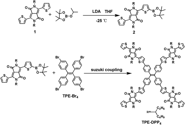
The synthetic routes to TPE-DPP4 are depicted in Scheme 1 (experimental details and the adopted synthetic route are provided in ESI†). A 3D twisted molecule based on TPE-DPP4 was obtained through Suzuki coupling between DDP-based DPP boric acid ester (compound 2) and tetra-brominated TPE (TPE-Br4). The resulting TPE-DPP4 was purified by column chromatography to obtain the product as a blue-black powder and the yield reached 80%. The structure of TPE-DPP4 was confirmed by time-of-flight mass spectroscopy as well as 1H and 13C NMR spectroscopy (related data of the intermediates and final product are shown in Fig. S1 and S2 of ESI†). Compared with the synthetic route of TPE-DPP4 depicted by Bhosale and coworkers33 (in which the TPE was first converted to TPE boric acid ester, followed by Suzuki coupling with brominated DPP), our method is simpler with a much higher yield. Compared with PCBM, which has poor solubility in common organic solvents, TPE-DPP4 has excellent solubility in DMF, hexane, dichloromethane, chloroform and tetrahydrofuran. The distinctly different solubility of TPE-PP4 and PCBM in DMF were compared (Fig. S3, ESI†). TPE-DPP4 (1 mg ml−1) showed a clear and stable solution, whereas a large amount of precipitate was formed in 0.5 mg ml−1 of PCBM. In addition, TPE-DPP4 possessed a similar 3D molecular structure to that of PCBM, and the 3D configuration of TPE-DPP4 was simulated by density functional theory (Fig. S4, ESI†).
The manufacturing procedure and architecture of PSCs are presented in Fig. 1. To ensure reproducibility of the performance, a conventional structure of FTO/compact-TiO2(c-TiO2)/mesoporous-TiO2(mp-TiO2)/CH3NH3PbI3 + TPE-DPP4/spiro-MeOTAD/Ag was employed. The perovskite hybrid film was fabricated by a two-step method. TPE-DPP4 served as an additive with concentrations of 0.01 and 0.02 wt% incorporated into PbI2 DMF solution to favor the growth of PbI2 film in the first step, followed by dipping into CH3NH3I (MAI) solution in the second step and annealing at 105 °C for 10 min. TPE-DPP4 also possesses a similar 3D structure to PCBM, so it may have a positive effect on the quality of CH3NH3PbI3.
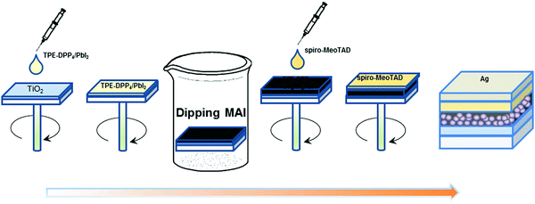 | ||
| Fig. 1 The spin-coating process for fabrication of perovskite solar cells with TPE-DPP4 using the structure of glass/FTO/c-TiO2/mp-TiO2/CH3NH3PbI3 + TPE-DPP4/spiro-MeOTAD/Ag. | ||
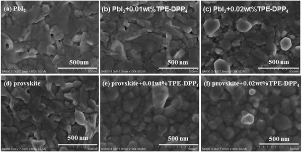
The morphology of the PbI2 + TPE-DPP4 hybrid films was first analyzed by scanning electron microscopy (SEM). Fig. 2(a–c) shows the representative morphological evolution of PbI2 films using different concentrations of TPE-DPP4. Both the size and number of holes decreased when a small amount of TPE-DPP4 was added to the PbI2 solution. A denser film could be attributed to TPE-DPP4 prolonging the precipitation/crystallization of the PbI2 film. Meanwhile, TPE-DPP4 could fill the hole of the PbI2 film in a similar to that of PCBM. The morphology of the PbI2 film (with and without TPE-DPP4) had a considerable impact on the morphology of the resulting perovskite film after addition of MAI, as displayed in Fig. 2(d–f). Incompact packing of CH3NH3PbI3 was significantly reduced and resulted in a more uniform and denser film when a small amount of TPE-DPP4 was added to the PbI2 solution. The perovskite + TPE-DPP4 hybrid films had a larger grain size than the pure perovskite film, which would be beneficial for the generation and transportation of charge carriers. In addition, the morphology of the perovskite films with or without TPE-DPP4 using atomic force microscopy (AFM) is shown in Fig. S5(a–c) (ESI†). The AFM results indicated that the film prepared with the TPE-DPP4 additive was more uniform with a larger domain size than the untreated perovskite film. This morphology characterization indicate that the introduction of TPE-DPP4 additive in the PbI2 solution can improve the film uniformity and perovskite crystallinity, two key requirements for high-performance PSCs.
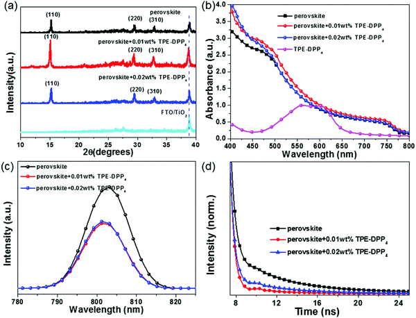
To investigate the change in crystallinity, X-ray diffraction (XRD) was performed (Fig. 3(a)). XRD patterns showed that the perovskite + TPE-DPP4 hybrid films and pure perovskite film had a similar profile, but the peak intensity was distinctly different between perovskite + TPE-DPP4 hybrid films and the pure perovskite film. The TPE-DPP4-incorporated perovskite films showed a higher diffraction peak intensity than the pure perovskite film at 15.2°, 29.2° and 32.7° assigned to (110), (220) and (310) diffractions of the tetragonal CH3NH3PbI3 phase, respectively. The enhanced intensity of the diffraction peak manifested as improved crystallinity of the CH3NH3PbI3 film. Extraordinarily, 0.01 wt% TPE-DPP4 showed the highest diffraction peak intensity. When the concentration of TPE-DPP4 increased from 0.01 wt% to 0.02 wt%, the peak intensity weakened, implying that high loading of TPE-DPP4 slightly affected the formation of the perovskite film. XRD results were in accordance with the SEM images.
The ultraviolet-visible (UV-vis) spectra of the pure perovskite film and perovskite + TPE-DPP4 films were further characterized. As shown in Fig. 3(b), all the perovskite films had strong absorption in the visible light range of 400–800 nm. Relative to pristine perovskite film, the perovskite film with TPE-DPP4 had stronger absorption, especially in the case of perovskite film with 0.01 wt% TPE-DPP4. The improved crystallinity of the TPE-DPP4-treated perovskite film as well as the good light absorption of TPE-DPP4 both made this contribution, which can ensure considerate current density in device performance.29,30
Fig. 3(c) shows the steady-state photoluminescence (PL) spectra of the pure perovskite film and perovskite + TPE-DPP4 hybrid films. When the films were excited at 400 nm (which had limited depth of penetration in the perovskite films), the PL emission peak appeared at 800 nm. It is obvious that the addition of the TPE-DPP4 additive dramatically quenched the intensity of the steady-state PL of the perovskite film, indicating a more efficient photo-generated electron separation in the perovskite + TPE-DPP4 hybrid films. To explore the true origin of quenched PL, the highest occupied molecular orbital (HOMO) and lowest unoccupied molecular orbital (LUMO) energy level were determined by cyclic voltammetry (CV). As displayed in Fig. S6(a) and Table S1 (ESI†), the HOMO and LUMO energy levels of TPE-DPP4 were estimated to be −5.26 eV and −3.63 eV, respectively. The valence band maximum and conduction band minimum of the CH3NH3PbI3 film were −5.43 eV and −3.92 eV, respectively. It was clearly observed that the energy level of TPE-DPP4 was well aligned with CH3NH3PbI3 (Fig. S6(b), ESI†). Therefore, TPE-DPP4 can act as an electron-donor to transfer electrons to CH3NH3PbI3 and provide an additional electron separation channel for PSCs. The active layer worked as BHJ CH3NH3PbI3 + TPE-DPP4 hybrid films rather than a pure light-active CH3NH3PbI3. Thereby, a more efficient electron transfer was observed by the dramatic PL quenching. To further understand the charge separation processes, the time-resolved PL was measured, as illustrated in Fig. 3(d). The perovskite +0.01 wt% TPE-DPP4 film give a shortest PL lifetime (4.87 ns) compared with the pristine perovskite film (5.01 ns) and perovskite +0.02 wt% TPE-DPP4 film (5.02 ns). The shortest PL lifetime was ascribed to the reduced charge trap state realized by enlarging the grain size and filling grain boundary of perovskite with the help of TPE-DPP4.
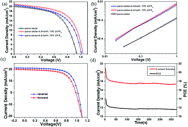
To explore the effect of TPE-DPP4 on PSCs performance, a device fabrication process is given in Fig. 1. The current density–voltage (J–V) curves of the device are shown in Fig. 4(a) and the relevant photovoltaic parameters are shown in Table 1. The photovoltaic performance varied with different concentrations of TPE-DPP4. For the pure CH3NH3PbI3 PSCs without TPE-DPP4, a PCE of 10.06% with an open circuit voltage (VOC) of 0.94 V, a short-circuit photocurrent density (JSC) of 20.06 mA cm−2, and a FF of 56.1% was observed. Intriguingly, the PCEs of the perovskite films with TPE-DPP4 additive devices were all enhanced compared with that of the control device, and the best PCE of 14.1% was achieved in the device with 0.01 wt% TPE-DPP4. In particular, all the device parameters improved with regard to FF (56.1% to 65.9%), JSC (20.06 to 21.04 mA cm−2) and VOC (0.94 to 1.02 V). The enhanced VOC, JSC and notable FF could be related to better crystallization and the perovskite film. The electron mobility of the pure and perovskite + TPE-DPP4 hybrid films was determined by the space-charge limited current method, as shown in Fig. 4(b). Clearly, with the addition of TPE-DPP4, the electron mobility of the perovskite + TPE-DPP4 hybrid films (1.1 × 10⁻⁵ cm2 V−1 s−1 for 0.01 wt% TPE-DPP4 and 1.0 × 10⁻⁵ cm2 V−1 s−1 for 0.02 wt% TPE-DPP4) was one order of magnitude higher than that of pure perovskite film (1.0 × 10⁻⁶ cm2 V−1 s−1). The improved mobility contributed to the higher JSC and FF. In Fig. 4(c), the device incorporated with perovskite +0.01 wt% TPE-DPP4 shows a PCE of 14.1% from the reverse scan, whereas the forward scan yields 12.1%. The perovskite +0.02 wt% TPE-DPP4 hybrid film had a similar hysteresis (Fig. S7, ESI†). Fig. 4(d) shows the device stability of a 0.01 wt% TPE-DPP4-based PSC under ambient conditions. It can be seen that the photocurrent and PCE stabilizes within seconds to approximately 17.33 mA cm−2 and 11.67%, probably due to TPE-DPP4 reacting with moving ions, just like PCBM.34,35 The integrated current density values from the external quantum efficiency (EQE) (Fig. S8, ESI†) curves of the perovskite, perovskite +0.01 wt% TPE-DPP4 and perovskite +0.02 wt% TPE-DPP4 were 17.86, 19.07 and 18.03 mA cm−2, respectively. Furthermore, the maximum values of the JSC from the EQE spectra were as almost the same as the J–V measurements even though there was little difference between the EQE and J–V measurements. This was because our tests were done under air atmosphere, leading to the decay of the device. Finally, the improved efficiencies of the devices were mostly attributed to the FF. Based on the above data and analysis, we believe that the photocurrents and efficiencies are credible.
| Active layer | J SC/mA cm−2 | V OC/V | FF/% | η/% |
|---|---|---|---|---|
| Perovskite +0 wt% | 20.06 | 0.94 | 56.1 | 10.6 |
| Perovskite +0.01 wt% | 21.04 | 1.02 | 65.9 | 14.1 |
| Perovskite +0.02 wt% | 20.61 | 1.01 | 55.6 | 11.6 |
In conclusion, we developed a novel 3D molecule, TPE-DPP4, as an additive for CH3NH3PbI3 to improve the performance of PSCs. It was found that the TPE-DPP4 appended to a CH3NH3PbI3 film could effectively improve the crystallinity of CH3NH3PbI3 by filling pinholes and vacancies between perovskite grains. TPE-DPP4 can also act as an additional electron-donor and light-capturer in perovskite. As a result, the PCE of PSCs with a TPE-DPP4 additive reached 14.1% with 40% enhancement compared with the pure perovskite device. This performance was not as high as the values reported by state-of-art devices but, due to the conventional device structure, higher efficiency could be achieved upon combination with device optimization. More importantly, this method provides a new, effective strategy to improve device performance by appending solution-processed 3D molecules as additives to the perovskite layer.
Acknowledgements
This work was financially supported by the National Science Fund for Distinguished Young Scholars (51425304), National Natural Science Foundation of China (51302130, 51663015, and 51673092), and Graduate Innovation Fund Projects of Jiangxi Province (YC2016-S005).Notes and references
- T. C. Sum and N. Mathews, Energy Environ. Sci., 2014, 7, 2518–2534 CAS.
- H.-S. Kim, C.-R. Lee, J.-H. Im, K.-B. Lee, T. Moehl, A. Marchioro, S.-J. Moon, R. Humphry-Baker, J.-H. Yum, J. E. Moser, M. Grätzel and N.-G. Park, Sci. Rep., 2012, 2, 591 Search PubMed.
- C. Ran, Y. Chen, W. Gao, M. Wang and L. Dai, J. Mater. Chem. A, 2016, 4, 8566–8572 CAS.
- A. Kojima, K. Teshima, Y. Shirai and T. Miyasaka, J. Am. Chem. Soc., 2009, 131, 6050–6051 CrossRef CAS PubMed.
- W. S. Yang, J. H. Noh, N. J. Jeon, Y. C. Kim, S. Ryu, J. Seo and S. I. Seok, Science, 2015, 348, 1234 CrossRef CAS PubMed.
- N. J. Jeon, J. H. Noh, W. S. Yang, Y. C. Kim, S. Ryu, J. Seo and S. I. Seok, Nature, 2015, 517, 476 CrossRef CAS PubMed.
- W. Y. Nie, H. H. Tsai, R. Asadpour, J. C. Blancon, A. J. Neukirch, G. Gupta, J. J. Crochet, M. Chhowalla, S. Tretiak, M. A. Alam, H. L. Wang and A. D. Mohite, Science, 2015, 347, 522 CrossRef CAS PubMed.
- T. Liu, F. Jiang, J. Tong, F. Qin, W. Meng, Y. Jiang, Z. Li and Y. Zhou, J. Mater. Chem. A, 2016, 4, 4305–4311 CAS.
- G. E. Eperon, V. M. Burlakov, P. Docampo, A. Goriely and H. J. Snaith, Adv. Funct. Mater., 2014, 24, 151 CrossRef CAS.
- Y. X. Zhao and K. Zhu, J. Am. Chem. Soc., 2014, 136, 12241 CrossRef CAS PubMed.
- F. Wang, H. Yu, H. Xu and N. Zhao, Adv. Funct. Mater., 2015, 25, 1120–1126 CrossRef CAS.
- W. Xu, J. A. McLeod, Y. Yang, Y. Wang, Z. Wu, S. Bai, Z. Yuan, T. Song, Y. Wang, J. Si, R. Wang, X. Gao, X. Zhang, L. Liu and B. Sun, ACS Appl. Mater. Interfaces, 2016, 8, 23181–23189 CAS.
- N. Yantara, F. Yanan, C. Shi, H. A. Dewi, P. P. Boix, S. G. Mhaisalkar and N. Mathews, Chem. Mater., 2015, 27, 2309 CrossRef CAS.
- W. Fu, J. Yan, Z. Zhang, T. Ye, Y. Liu, J. Wu, J. Yao, C. Z. Li, H. Li and H. Chen, Nano Lett., 2013, 13, 1764 CrossRef PubMed.
- H. B. Kim, H. Choi, J. Jeong, S. Kim, B. Walker, S. Song and J. Y. Kim, Nanoscale, 2014, 6, 6679–6683 RSC.
- N. J. Jeon, J. H. Noh, Y. C. Kim, W. S. Yang, S. Ryu and S. Il Seol, Nat. Mater., 2014, 13, 897 CrossRef CAS PubMed.
- Y. G. Rong, Z. J. Tang, Y. F. Zhao, X. Zhong, S. Venkatesan, H. Graham, M. Patton, Y. Jing, A. M. Guloy and Y. Yao, Nanoscale, 2015, 7, 10595 RSC.
- Y. H. Chen, T. Chen and L. M. Dai, Adv. Mater., 2015, 27, 1053 CrossRef CAS PubMed.
- M. Ramesh, K. M. Boopathi, T. Y. Huang, Y. C. Huang, C. S. Tsao and C. W. Chu, ACS Appl. Mater. Interfaces, 2015, 7, 2359 CAS.
- Z. G. Xiao, C. Bi, Y. C. Shao, Q. F. Dong, Q. Wang, Y. B. Yuan, C. G. Wang, Y. L. Gao and J. S. Huang, Energy Environ. Sci., 2014, 7, 2619 CAS.
- E. Gracia-Espino, H. R. Barzegar, A. M. Yan, A. Zettl and T. Wagberg, ACS Nano, 2015, 9, 10516 CrossRef CAS PubMed.
- Z. Xiao, C. Bi, Y. Shao, Q. Dong, Q. Wang, Y. Yuan, C. Wang, Y. Gao and J. Huang, Energy Environ. Sci., 2014, 7, 2619 CAS.
- M. Liu, M. B. Johnston and H. J. Snaith, Nature, 2013, 501, 395 CrossRef CAS PubMed.
- C. T. Zuo and L. M. Ding, Nanoscale, 2014, 6, 9935–9938 RSC.
- P. W. Liang, C. Y. Liao, C. C. Chueh, F. Zuo, S. T. Williams, X. K. Xin, J. J. Lin and A. K. Y. Jen, Adv. Mater., 2014, 26, 3748–3754 CrossRef CAS PubMed.
- C. X. Ran, Y. H. Chen, W. Y. Gao, M. Q. Wang and L. M. Dai, J. Mater. Chem. A, 2016, 4, 8566–8572 CAS.
- Y. Zhang, L. Tan, Q. Fu, L. Chen, T. Ji, X. Hu and Y. Chen, Chem. Commun., 2016, 52, 5674–5677 RSC.
- C.-H. Chiang and C.-G. Wu, Nat. Photonics, 2016, 10, 196–200 CrossRef CAS.
- M. S. Vezie, S. Few, I. Meager and J. Nelson, Nat. Mater., 2016, 15, 746–753 CrossRef CAS PubMed.
- H. J. Bin, Z. G. Zhang, L. Gao and Y. F. Li, J. Am. Chem. Soc., 2016, 138, 4657–4664 CrossRef CAS PubMed.
- Z.-F. Chang, L.-M. Jing, B. Chen, M. Zhang, X. Cai, J.-J. Liu, Y.-C. Ye, X. Lou, Z. Zhao, B. Liu, J.-L. Wang and B. Z. Tang, Chem. Sci., 2016, 7, 4527–4536 RSC.
- J.-L. Wang, Z. Wu, J.-S. Miao, K.-K. Liu, Z.-F. Chang, R.-B. Zhang, H.-B. Wu and Y. Cao, Chem. Mater., 2015, 27, 4338–4348 CrossRef CAS.
- A. Rananaware, A. Gupta, J. Li, A. Bilic, L. Jones, S. Bhargava and S. V. Bhosale, Chem. Commun., 2016, 52, 8522–8525 RSC.
- A. Guerrero, J. You, C. Aranda, Y. S. Kang, G. Garcia-Belmonte, H. Zhou, J. Bisquert and Y. Yang, ACS Nano, 2016, 10, 218–224 CrossRef CAS PubMed.
- J. Carrillo, A. Guerrero, S. Rahimnejad, O. Almora, I. Zarazua, E. Mas-Marza, J. Bisquert and G. Garcia-Belmonte, Adv. Energy Mater., 2016, 6, 1502246 CrossRef.
Footnotes |
| † Electronic supplementary information (ESI) available. See DOI: 10.1039/c6qm00210b |
| ‡ B. Huang and Q. Fu contributed equally to this work. |
| This journal is © the Partner Organisations 2017 |

