Temperature assisted shear exfoliation of layered crystals for the large-scale synthesis of catalytically active luminescent quantum dots†
Shubhadeep
Pal
a,
Kiran Kumar
Tadi
a,
P. M.
Sudeep
ab,
Sruthi
Radhakrishnan
b and
Tharangattu N.
Narayanan
*a
aTIFR-Center for Interdisciplinary Sciences (TCIS), Tata Institute of Fundamental Research, 21 Brundavan Colony, Narsingi, Hyderabad, 500075, India. E-mail: tnn@tifrh.res.in
bDepartment of Materials Science & NanoEngineering, Rice University, Houston, Texas 77005, USA
First published on 11th August 2016
Abstract
Edge state manipulations of transition metal dichalcogenides of ultra-small sizes are receiving tremendous scientific interest due to their applications in electronics, optoelectronics and energy conversion technologies. Here, we report a novel single step route for the large-scale production of luminescent quantum dots (QDs) of layered materials using a temperature assisted shear exfoliation method. The syntheses of molybdenum disulfide (MoS2) and tungsten disulfide (WS2) QDs are demonstrated, and enhanced hydrogen evolution reaction catalytic activities of QDs in comparison to their bulk and layered counterparts are demonstrated. This synthesis strategy is generalized to other layered structures such as graphite, leading to a bulk production of luminescent monodispersed QDs, enabling their status to the technology readiness level 9.
1. Introduction
One of the clean energy, processes without the emission of carbon dioxide, which leads to the production of a renewable energy source, hydrogen (H2), is the hydrogen evolution reaction (HER) which is receiving tremendous attention from the scientific community.1–5 Due to the inherent sluggishness of this reaction, HER demands the use of catalysts for the efficient production of H2.5,6 Commercial electrocatalytic systems for H2 production rely on the use of noble metals such as platinum (Pt), but their high cost and limited worldwide availability make this energy technology formidable.7,8 Hence the search for non-metal or noble metal free HER catalysts is receiving huge interest in recent times. The Sabatier principle states that the interactions between catalysts and reactants should not be too strong or weak to precede catalytic reaction efficiently, and a high free energy adsorption value will result in weak binding of ligands to the catalytic sites rendering adsorption as a rate determining step in the reaction.9,10 Strong adsorption will result in poor conversion, leading to the poisoning of the catalytic sites. This excludes many metals from being used for HER catalysis. Density functional theory based calculations suggest that the criterion for a material to be a good catalyst is that the free energy of adsorbed H should be close to that of the reactant or the product (i.e., ΔGH = 0), and the calculations for transition metal dichalcogenides (TMCs) such as molybdenum disulfide (MoS2) suggest that they are thermo-neutral, making them potentially promising HER catalysts.11,12Advent of layered TMCs opens new avenues in electronics and energy technologies. Interesting optical, semiconducting and catalytic properties of TMCs are finding applications in photovoltaics, transistors, sensors, and electro- and photo-catalysis.13,14 Atomically layered TMCs such as MoS2, tungsten disulfide (WS2) etc. have been identified as promising catalysts, particularly for the HER, since all the catalytically active sites are exposed due to their layered nature and they show tunable catalytic activities due to compositional and crystal structure control, strain and edge manipulation capabilities.15 Bulk TMCs show sluggish catalytic activity due to a few active sites and poor conductivity; hence efforts are being made to engineer the catalytic activities of TMCs by nanostructuring.
It has been reported that the catalytically active sites of MoS2 and other TMCs are located along their edges, and basal planes are ineffective for catalytic reactions. Hence nano-engineering of single/a few layered MoS2 with an effective exposure of edges will be a unique method for enhanced electrochemical activities. Among various nanostructures such as nanoparticles, nanorods, films, quantum dots (QDs) etc., QDs having one or a few layers are the most favorable candidates for catalysis.16 But, synthesis methods for TMC QDs are not well explored, and the reported techniques are time consuming and need tedious multi-step (synthesis of atomic layers and their further cutting) processes.17 Hydrothermal cutting and sonication, electrochemical routes, inverse micellar cage based synthesis etc. are a few reported techniques for the QD synthesis of layered materials.
Development of shear exfoliation based defect free atomic layer synthesis from bulk crystals opened a platform for the large-scale production of two-dimensional (2D) crystals, enabling TMCs or other 2D materials to be of the technology readiness level 9 (TRL9).18 Here we employ a modified shear exfoliation process which leads to the large scale production of monodispersed luminescent QDs of MoS2 and WS2. A reaction mechanism has been put forward for the production of QDs from bulk crystals, and these QDs are studied for their HER efficacy. Their HER properties are compared with bulk crystals, exfoliated sheets, and other reports on similar QDs. The synthesis method has been extended to graphite, yielding the bulk luminescent graphene QDs from commercial graphite crystals.
2. Experimental
2.1 Materials and characterization
Bulk crystals of MoS2 (6 µm), WS2 (6 µm), and graphite (2 µm) were purchased from Sigma-Aldrich. Dimethyl formamide (DMF) of analytical reagent grade was procured from Merck chemicals. Ultrapure Milli-Q water (18.2 MΩ) was used in all experiments. A Silverson model L5M high-shear mixer (Fig. 1 (left)) with a circular hole stator was used for mechanical exfoliation of crystals. A Jasco V-670 spectrometer was used to collect the absorption spectra of samples. The steady state luminescence properties of the samples were monitored using Quanta Master 400 (Photon Technology International). High resolution transmission electron microscope (HRTEM) images were obtained using a JEOL JEM 2010 field emission gun transmission electron microscope with an accelerating voltage of 200 kV. X-ray photoelectron spectroscopy (XPS) data were collected on a Thermo scientific photoemission spectrometer. Atomic force microscope (AFM) measurements were conducted using an AFM Workshop model SA-SFM (CA, USA) in the non-contact mode by drop casting the diluted dispersion sample on atomically smooth synthetic mica flakes. Raman spectra of the samples were recorded using a Witec Micro Raman spectrometer model alpha300 RA with an excitation wavelength of 488 nm.2.2 Synthesis of QDs
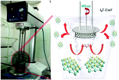
MoS2/WS2 crystals were mixed with dimethyl formamide (DMF, 0.5 g in 250 mL) and this mixture was homogenized using a high shear mixer. Various shear rates were attempted and it was found that 5000 rpm for 1 hour shearing leads to the formation of layered sheets from the bulk crystals, which is in accordance with the earlier report.18 As reported by Parton et al.,18 the yield of the sheets is increased with the rotation speed and in the present study, the sheet production is optimized for 8000 rpm for 3 hours. The same reaction was conducted at elevated temperatures too by keeping the shearing system in a thermal bath at constant temperature. The photograph of the real time experimentation and schematic of shearing are shown in Fig. 1. The resulting products are found to be highly dispersed in DMF and they are collected and further characterized using various techniques. The same method is optimized for graphite crystals too and the results are shown in the ESI.†2.3 Electrochemical studies
To prepare working electrodes for electrochemical measurements the synthesized QDs/nanosheets (5 µL) were drop-casted onto a freshly polished glassy carbon electrode (GCE) and dried under ambient conditions. The working electrode was inserted into a three-electrode system consisting of a spiral platinum wire as a counter electrode and Ag/AgCl (3.0 M) as a reference electrode. The electrochemical tests were carried out on a BioLogic SP-300 work station. Prior to the test, the electrolyte (0.5 M H2SO4) was saturated under N2 flow for 30 minutes. Linear sweep voltammetry (LSV) was conducted at a scan rate of 5 mV s−1. Electrochemical impedance studies (EIS) were performed in a redox mixture consisting of 5 mM [Fe(CN)6]3− and 5 mM [Fe(CN)6]4− in 0.1 M KCl as supporting electrolytes. The working electrode was held at a half-wave peak potential of the redox probe over the frequency range 105–0.1 Hz with a small excitation peak-to-peak amplitude of 10 mV. A long-term durability test was also conducted for different samples by using a chronoamperometric technique.3. Results and discussion
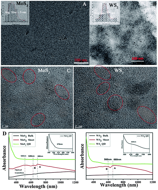
Three types of morphologies, namely bulk, sheet, and QD, of the same material (MoS2/WS2) were used for comparative studies. A schematic of the sheet and the QD synthesis process from the bulk crystal is demonstrated in Fig. 1 (right). Room temperature (kBT ∼ 25 meV) exfoliation leads to the production of exfoliated sheets (TEM images are shown in the ESI,† Fig. S1), while high temperature (100 °C, kBT ∼ 32 meV) shear exfoliation leads to the production of well dispersed liquids (ESI,† Fig. S2), indicating the production of a large amount of monodispersed QDs (Fig. 2A and B) having an average size of 5 nm. The same phenomenon is observed in the case of graphite too, where elevated temperature exfoliation leads to the formation of graphene QDs while room temperature shear exfoliation leads to nanosheets, ESI,† Fig. S3. The mechanism of room temperature shear exfoliation in low surface tension liquids leading to atomic layers has been recently well studied.18 In shear exfoliation, after a critical rate, bulk layered crystals start to delaminate layer by layer with the aid of shear force generated by liquid at the liquid crystal interface, those exfoliated layers can be dispersed in liquids having matching surface free energy. The mechanism leading to the QD formation while shearing at high temperature is discussed in the later section.The HRTEM images of MoS2 and WS2 QDs are shown in Fig. 2(C). The lattice planes of the crystals are matched with the reported values (interplanar distance (d) values of 0.27 nm and 0.16 nm correspond to (100) and (110) respectively for hexagonal MoS2 and WS2 crystals17) and the planes shown in the figure indicate the crystallinity of QDs. The average size of QDs is found to be ∼5 nm (particle size histograms are provided in Fig. 2A and B insets and the ESI,† Fig. S4) as it is further confirmed from the HRTEM images; red circles shown indicate one QD crystal. Low resolution images of QDs are given in the ESI,† Fig. S4, indicating the large scale production of QDs via this technique. AFM measurements were conducted on drop casted QD samples over atomically smooth mica film. For MoS2 samples, the AFM data (Fig. S5, ESI†) show that the average thickness of the QDs is ∼4 nm indicating that 4–5 atomic layers are present in a single QD. In the case of WS2 QDs, the step height profile of layers is about 2–4 nm suggesting that 3–4 atomic layers are present in a single QD.
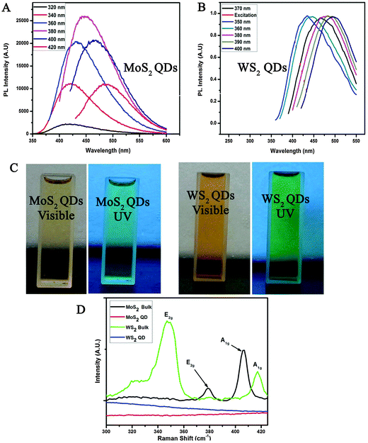
The UV-Vis absorption spectra of various samples are given in Fig. 2D. Bulk MoS2 has a broad absorbance over the entire visible range. In the case of exfoliated sheets, the emergence of A and B excitonic transitions can be observed at 688 nm and 628 nm, respectively19 and a broad absorption band between 520 and 420 nm indicates the optical transition in the multiple minima of density of states both in valence and conduction bands.20 But in the case of QDs, clear opening up of the bandgap resulting in a shift and broadening of the excitonic transitions are observed.20 These are the signatures of quantum dots formation due to the increase in the energy gap at the K point in the Brillouin zone. Similar effects are observed in WS2 QDs too.21 Furthermore, it has been reported that the large spin-valley coupling (as observed from UV-Vis spectra) of TMC QDs can show PL emission in the green region.22 The PL spectra have been recorded for MoS2 QDs (Fig. 3A) and WS2 QDs (Fig. 3B). The emission spectra of MoS2 QDs are recorded at various excitation wavelengths ranging 320–420 nm with an interval of 20 nm and 370–400 nm for WS2. Later it is proven that these QDs also contain oxygen functionalities at the edges. Bulk or sheets do not show any PL characteristics (ESI,† Fig. S6) indicating that the temperature assisted exfoliation in DMF aids the cutting of sheets to QDs via edge oxidation, as it is further proved through X-ray photoelectron spectroscopy (XPS).
The photographs of the as synthesized QDs on DMF under visible and UV-light illumination are shown in Fig. 3C. It is observed that the QDs are highly stable and show green fluorescence when irradiated with 350 nm UV-light. This green light luminescence observation is in accordance with the above-mentioned PL results indicating the emission peak of ∼490–510 nm.
The Raman spectra of bulk MoS2/WS2 and their corresponding QDs are shown in Fig. 3D. The Raman spectrum of bulk MoS2 shows two phonon modes of E2g and A1g at 379 cm−1 and 407 cm−1 corresponding to in-plane and out-of-plane vibrations of Mo–S as viewed along the [100] direction respectively.23 Bulk WS2 also shows two documented peaks: an in-plane (E2g) mode located around ∼348 cm−1 and an out-of-plane (A1g) mode which is located around 417 cm−1.24 But MoS2/WS2 QDs do not show peaks corresponding to in-plane (E2g) or out-of-plane (A1g) modes as the vibration modes are confined by the grain distribution and the domain size of QDs.23,25
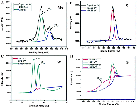
XPS measurements were carried out to investigate the chemical composition of QDs. MoS2 exhibits Mo 3d5/2 and 3d5/2 binding energies at 229.4 eV and 232.5 eV respectively.26 From Fig. 4A, the deconvoluted spectra of Mo show two broad peaks corresponding to the binding energies centered at ∼232 eV and ∼235.2 eV indicating the mixed valences of +4 and +5. The W in WS2 XPS spectrum (Fig. 4C) shows two sharp peaks at binding energies 35.1 eV (W 4f 7/2) and 37.2 eV (W 4f 5/2). This is well in accordance with W4+ species of highly crystalline 2H–WS2. In the XPS spectra of ‘S’ in both MoS2 and WS2 (Fig. 4B and D), two peaks are observed at ∼161.6 eV and ∼162.8 eV corresponding to S 2p 3/2 and 2p 1/2, respectively. An additional peak at a high binding energy of ∼168 eV shows the presence of S–O bonds, which could have resulted from the partial oxidation of the edged chalcogen of MoS2/WS2 in the presence of DMF solvent at 100 °C temperature during the synthesis. This indicates that the QDs prepared by this technique are highly edge oxidized and this oxidation is the leading mechanism for the QD formation. But the XPS data of room temperature shear exfoliated layers show the absence of oxidation (Fig. S6, ESI†). These oxygen edge states are further responsible for excitation dependent PL as observed in the above section.
The UV-Vis absorption spectrum of graphene QDs (GQDs) is shown in Fig. S7 (ESI†). A strong absorption peak centered at 270 nm is due to the π–π* transition in aromatic C![[double bond, length as m-dash]](https://www.rsc.org/images/entities/char_e001.gif) C bonds. The PL emission from GQDs can be due to intrinsic (due to quantum confinement) and defect state emissions.27 The excitation dependent emission properties observed in the present study indicate that the oxygen containing defect states play a crucial role in the PL emission mechanism (UV-Vis NIR spectrum of GQDs shows an absorption band edge at ∼375 nm while excitation dependent PL spectra were exhibited by GQDs with a maximum emission intensity corresponding to 375 nm excitation).
C bonds. The PL emission from GQDs can be due to intrinsic (due to quantum confinement) and defect state emissions.27 The excitation dependent emission properties observed in the present study indicate that the oxygen containing defect states play a crucial role in the PL emission mechanism (UV-Vis NIR spectrum of GQDs shows an absorption band edge at ∼375 nm while excitation dependent PL spectra were exhibited by GQDs with a maximum emission intensity corresponding to 375 nm excitation).
Altering electronic properties of pristine MoS2/WS2 due to oxidation could help in the generation of active surface states with highly catalytic reactivity towards the hydrogen evolution reaction. Since MoS2 nanosheets and QDs are well known for their HER due to the presence of active edge sites, the electrocatalytic HER activity of MoS2/WS2 is studied by measuring linear sweep voltammograms in N2 saturated 0.5 M H2SO4 using 5 µL of the QDs coated on the glassy carbon (GC) electrode as the working electrode. Similar measurements are also conducted by using MoS2/WS2 nanosheets and the bulk MoS2/WS2 coated GC electrode. It is obvious from the cathodic polarization curves (Fig. 5A and C) that bulk MoS2/WS2 shows very weak HER performance with high on-set potentials (η) (∼0.6 V vs. RHE) and small cathodic current densities. In contrast, as the size of MoS2 changes from bulk to nanosheets and QDs, the on-set potential for HER activity decreases towards positive potentials (MoS2 nanosheets ∼0.4 V, MoS2 QDs ∼0.3 V and WS2 QDs 0.5 V) with high cathodic current densities.
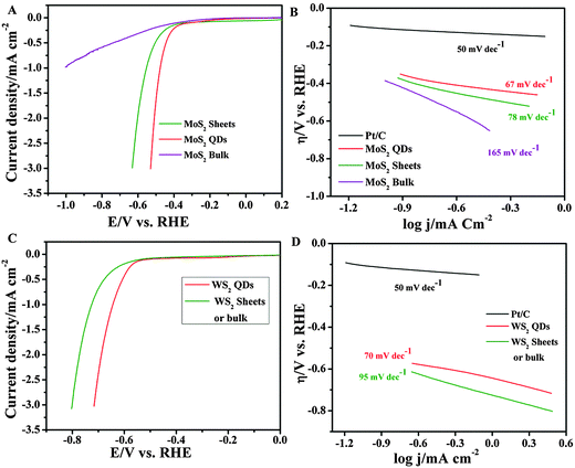 | ||
| Fig. 5 HER studies on MoS2 and WS2: (A) and (C) HER polarization curves in 0.5 M H2SO4 for MoS2 and WS2 respectively. The corresponding Tafel slopes are given in (B) and (D). | ||
There are three principle steps for evolution of hydrogen in acidic medium.28,29 The primary step involves discharging of a hydrogen atom (i.e., Volmer reaction eqn (1))
| H3O+ + e− → Hads + H2O | (1) |
| Hads + H3O+ + e− → H2 + H2O | (2) |
| Hads + Hads → H2 | (3) |
![[thin space (1/6-em)]](https://www.rsc.org/images/entities/char_2009.gif) log|j| + a, where j is current density and b is the Tafel slope) for determining the corresponding Tafel slopes. As shown in Fig. 5B, the obtained Tafel slope of the Pt catalyst is 50 mV dec−1 and is similar to the previous literature.30 For MoS2 QDs and WS2 QDs the slopes are found to be 60 mV dec−1 and 67 mV dec−1 respectively. The values are found to be much smaller than that of the corresponding bulk or nano-sheet materials. The exchange current densities (j0) estimated by extrapolating the Tafel plots of MoS2 and WS2 QDs are found to be 0.71 µA cm−2 and 0.67 µA cm−2 respectively. The value of the Tafel slope of MoS2 QDs is smaller than the reported Tafel slopes for defect-free MoS2 nanosheets (87 mV dec−1),31 nanosized bulk MoS2 (82 mV dec−1)32 and MoS2 nanoparticles (77 mV dec−1).33 These results reflect the participation of active edge sites in highly reversible hydrogen ion adsorption along with the enhanced active surface area for HER electrocatalytic activity.34–37
log|j| + a, where j is current density and b is the Tafel slope) for determining the corresponding Tafel slopes. As shown in Fig. 5B, the obtained Tafel slope of the Pt catalyst is 50 mV dec−1 and is similar to the previous literature.30 For MoS2 QDs and WS2 QDs the slopes are found to be 60 mV dec−1 and 67 mV dec−1 respectively. The values are found to be much smaller than that of the corresponding bulk or nano-sheet materials. The exchange current densities (j0) estimated by extrapolating the Tafel plots of MoS2 and WS2 QDs are found to be 0.71 µA cm−2 and 0.67 µA cm−2 respectively. The value of the Tafel slope of MoS2 QDs is smaller than the reported Tafel slopes for defect-free MoS2 nanosheets (87 mV dec−1),31 nanosized bulk MoS2 (82 mV dec−1)32 and MoS2 nanoparticles (77 mV dec−1).33 These results reflect the participation of active edge sites in highly reversible hydrogen ion adsorption along with the enhanced active surface area for HER electrocatalytic activity.34–37
Electrochemical impedance spectroscopy (EIS) is an efficient technique to determine the heterogeneous electron transfer resistance (Rct) between the electrode and the electrolyte. The impedance studies were performed in 5 mM K3[Fe(CN)6] and 5 mM K4[Fe(CN)6] as an inner redox probe consisting of 0.1 M KCl supporting electrolyte at the open circuit potential with a small excitation amplitude of 10 mV (Fig. S8, ESI†). The Rct value of the modified GC surface is determined from the semicircle diameter of the obtained Nyquist plot by fitting with a Randles equivalent circuit. The plots in Fig. S7 (ESI†) show higher Rct values for bulk MoS2 (920 Ω) and bulk WS2 (715 Ω) than their respective QDs. The resultant QDs show considerably small Rct values (475 Ω in the case of MoS2 and 205 Ω in the case of WS2).
Chronoamperometry studies on QD modified electrodes were conducted for the HER, ensuring the stability of the catalysts towards the HER process. As shown in Fig. S9 (ESI†), at the overpotentials of 0.4 V for MoS2 QDs and 0.6 V for WS2 QDs, the current density remains stable for more than 13 hours. This durability test shows the promise of these QD based nanostructured catalysts for practical applications.
4. Conclusions
A novel temperature assisted shear exfoliation method is demonstrated for the synthesis of monodispersed QDs. This method leads to the high yield production of luminescent QDs (∼5 nm lateral width with 3–5 atomic layers) of layered materials directly from their bulk crystals. Elevated temperatures aid the edge oxidation of crystals in solvents such as DMF, and these defective oxidized centers help to cut the sheets by shearing. This single step QD production method is demonstrated for TMC crystals such as MoS2 and WS2, and then extended to graphite. MoS2 and WS2 QDs were demonstrated for their enhanced catalytic activities towards the HER in comparison to their bulk and layered counterparts, indicating the importance of nano- engineering in electrocatalysis.Acknowledgements
Authors acknowledge TIFR-Centre for Interdisciplinary Sciences (TCIS), Hyderabad, India for the financial support. Authors thank Prof. P. M. Ajayan, Rice University, USA for allowing to use the TEM facility.References
- H. Fei, J. Dong, M. J. Arellano-Jiménez, G. Ye, N. D. Kim, E. L. G. Samuel, Z. Peng, Z. Zhu, F. Qin, J. Bao, M. J Yacaman, P. M. Ajayan, D. Chen and J. M. Tour, Nat. Commun., 2015, 6, 1–8 Search PubMed.
- D. Voiry, H. Yamaguchi, J. Li, R. Silva, D. C. B. Alves, T. Fujita, M. Chen, T. Asefa, V. B. Shenoy, G. Eda and M. Chhowalla, Nat. Mater., 2013, 12, 850–855 CrossRef CAS PubMed.
- S. Xu, D. Li and P. Wu, Adv. Funct. Mater., 2015, 25, 1127–1136 CrossRef CAS.
- L. V. Mattos, G. Jacobs, B. H. Davis and F. B. Noronha, Chem. Rev., 2012, 112, 4094–4123 CrossRef CAS.
- X. Chen, S. Shen, L. Guo and S. S. Mao, Chem. Rev., 2010, 110, 6503–6570 CrossRef CAS.
- A. J. Esswein and D. G. Nocera, Chem. Rev., 2007, 107, 4022–4047 CrossRef CAS.
- B. C. H. Steele and A. Heinzel, Nature, 2001, 414, 345–352 CrossRef CAS.
- R. Bashyam and P. Zelenay, Nat. Lett., 2006, 443, 63–66 CrossRef CAS.
- P. J. Rheinlander, J. Herranz, J. Durst and H. A. Gasteiger, J. Electrochem. Soc., 2014, 161, 1448–1457 CrossRef.
- M. C. Tavares, S. A. S. Machado and L. H. Mazo, Electrochim. Acta, 2001, 46, 4359–4369 CrossRef CAS.
- S. Dou, J. Wu, L. Tao, A. Shen, J. Huo and S. Wang, Nanotechnology, 2016, 27, 1–6 Search PubMed.
- Z. Wu, B. Fang, A. Bonakdarpour, A. Sun, D. P. Wilkinsonb and D. Wang, Appl. Catal., B, 2012, 125, 59–66 CrossRef CAS.
- P. Kumar Shah, T. N. Narayanan, C.-Z. Li and S. Alwarappan, Nanotechnology, 2015, 26, 315102 CrossRef.
- T. N. Narayanan, C. Vusa and S. Alwarappan, Nanotechnology, 2014, 25, 335702 CrossRef.
- D. Voiry, J. Yang and M. Chhowalla, Adv. Mater., 2016 DOI:10.1002/adma.201505597.
- Y. T. Liang, B. K. Vijayan, O. Lyandres, K. A. Gray and M. C. Hersam, J. Phys. Chem. Lett., 2012, 3, 1760–1765 CrossRef CAS.
- D. Gopalakrishnan, D. Damien, B. Li, H. Gullappalli, V. K. Pillai, P. M. Ajayan and M. M. Shaijumon, Chem. Commun., 2015, 51, 6233–6440 RSC.
- M. Moebius, H. Pettersson, E. Long, J. Coelho, S. E. O'Brien, E. K. McGuire, B. Mendoza Sanchez, G. S. Duesberg, N. McEvoy, T. J. Pennycook, C. Downing, A. Crossley, V. Nicolosi and J. N. Coleman, Nat. Mater., 2014, 13, 624–630 CrossRef.
- A. Kumar Mishra, K. V. Lakshmi and L. Huang, Sci. Rep., 2015, 5, 15718 CrossRef.
- X. Wang, G. Sun, N. Li and P. Chen, Chem. Soc. Rev., 2016, 45, 2239–2262 RSC.
- L. Lin, Y. Xu, S. Zhang, I. M. Ross, A. C. M. Ong and D. A. Allwood, ACS Nano, 2013, 7, 8214–8223 CrossRef CAS.
- H. Lin, C. Wang, J. Wu, Z. Xu, Y. Huang and C. Zhang, New J. Chem., 2015, 39, 8492–8497 RSC.
- M. Ye, D. Winslow, D. Zhang, R. Pandey and Y. Khin Yap, Photonics, 2015, 2, 288–307 CrossRef.
- W. Zhao, Z. Ghorannevis, K. K. Amara, J. R. Pang, M. Toh, X. Zhang, C. Kloc, P. Heng Tane and G. Eda, Nanoscale, 2013, 5, 9677–9683 RSC.
- H. Li, Q. Zhang, C. Chong Ray Yap, B. Kang Tay, T. Hang Tong Edwin, A. Olivier and D. Baillargeat, Adv. Funct. Mater., 2012, 22, 1385–1390 CrossRef CAS.
- H. Li, K. Yu, C. Li, B. Guo, X. Lei, H. Fu and Z. Zhu, J. Mater. Chem. A, 2015, 3, 20225–20235 CAS.
- L. Li, G. Wu, G. Yang, J. Peng, J. Zhao and J.-J. Zhu, Nanoscale, 2013, 5, 4015–4039 RSC.
- N. Pentland, J. O. M. Bockris and E. Sheldon, J. Electrochem. Soc., 1957, 104, 182–194 CrossRef CAS.
- B. E. Conway and B. V. Tilak, Electrochim. Acta, 2002, 47, 3571–3594 CrossRef CAS.
- Y. Li, H. Wang, L. Xie, Y. Liang, G. Hong and H. Dai, J. Am. Chem. Soc., 2011, 133, 7296–7299 CrossRef CAS PubMed.
- A. B. Laursen, P. C. K. Vesborg and I. Chorkendorf, Adv. Mater., 2013, 25, 5807–5813 CrossRef PubMed.
- Z. Wu, B. Fang, Z. Wang, C. Wang, Z. Liu, F. Liu, W. Wang, A. Alfantazi, D. Wang and D. P. Wilkinson, ACS Catal., 2013, 3(9), 2101–2107 CrossRef CAS.
- X. Ren, L. Pang, Y. Zhang, X. Ren, H. Fana and S. (Frank) Liu, J. Mater. Chem. A, 2015, 3, 10693–10697 CAS.
- A. B. Laursen, P. C. K. Vesborgand and I. Chorkendorff, Chem. Commun., 2013, 49, 4965–4967 RSC.
- J. Xie, H. Zhang, S. Li, R. Wang, X. Sun, M. Zhou, J. Zhou, X. W. Lou and Y. Xie, Adv. Mater., 2013, 25, 5807–5813 CrossRef CAS.
- D. Gopalakrishnan, D. Damien and M. M. Shaijumon, ACS Nano, 2014, 8, 5297–5303 CrossRef CAS.
- F. Li, J. Li, Z. Cao, X. Lin, X. Li, Y. Fang, X. An, Y. Fu, J. Jin and R. Li, J. Mater. Chem. A, 2015, 3, 21772–21778 CAS.
Footnote |
| † Electronic supplementary information (ESI) available. See DOI: 10.1039/c6qm00081a |
| This journal is © the Partner Organisations 2017 |

