
High temperature thermal management with boron nitride nanosheets†
Yilin
Wang‡
a,
Lisha
Xu‡
a,
Zhi
Yang‡
b,
Hua
Xie
a,
Puqing
Jiang
c,
Jiaqi
Dai
a,
Wei
Luo
a,
Yonggang
Yao
a,
Emily
Hitz
a,
Ronggui
Yang
c,
Bao
Yang
b and
Liangbing
Hu
 *a
*a
aDepartment of Materials Science and Engineering, University of Maryland, College Park, Maryland 20742, USA. E-mail: binghu@umd.edu
bDepartment of Mechanical Engineering, University of Maryland, College Park, Maryland 20742, USA
cDepartment of Mechanical Engineering, University of Colorado, Boulder, Colorado 80309, USA
First published on 15th November 2017
Abstract
The rapid development of high power density devices requires more efficient heat dissipation. Recently, two-dimensional layered materials have attracted significant interest due to their superior thermal conductivity, ease of production and chemical stability. Among them, hexagonal boron nitride (h-BN) is electrically insulating, making it a promising thermal management material for next-generation electronics. In this work, we demonstrated that an h-BN thin film composed of layer-by-layer laminated h-BN nanosheets can effectively enhance the lateral heat dissipation on the substrate. We found that by using the BN-coated glass instead of bare glass as the substrate, the highest operating temperature of a reduced graphene oxide (RGO) based device could increase from 700 °C to 1000 °C, and at the same input power, the operating temperature of the RGO device is effectively decreased. The remarkable performance improvement using the BN coating originates from its anisotropic thermal conductivity: a high in-plane thermal conductivity of 14 W m−1 K−1 for spreading and a low cross-plane thermal conductivity of 0.4 W m−1 K−1 to avoid a hot spot right underneath the device. Our results provide an effective approach to improve the heat dissipation in integrated circuits and high power devices.
Introduction
With the scaling down of device dimensions of integrated circuits and high power electronics,1 heat dissipation has become one of the most critical challenges in device performance and reliability.2–6 If the temperature exceeds the normal operating range, the performance of the device will be degraded and the device may even fail. Therefore, heat spreading ability of the substrate hosting the devices becomes critical. The heat spreading capability of a material directly depends on its thermal conductivity. At room temperature the thermal conductivities of materials most commonly used in electronics ranges from 0.2 W m−1 K−1 (ref. 7) for polymers to ∼2000 W m−1 K−1 (ref. 8 and 9) for synthetic diamond. Recently, two-dimensional materials,10–13 such as graphene and hexagonal boron nitride (h-BN) have attracted significant attention due to their remarkable thermal conductivity, making them promising as thermal management materials.14–22 The in-plane thermal conductivity of single-layer graphene at room temperature is in a range of 2000–5000 W m−1 K−1,23–29 which is the highest among the known materials. Even under various engineering configurations, the thermal conductivity of few-layer graphene is still much better than the commonly used materials, such as copper and silicon, which has thus attracted a lot of interests. However, graphene is electrically conductive, and it cannot be used as the thermal management material directly beneath the devices.Although h-BN has a hexagonal honeycomb lattice structure similar to graphene,30,31 it is electrically insulating with a large band gap of 5.8 eV.32,33 The calculated in-plane thermal conductivity for h-BN can reach 2000 W m−1 K−1.15,34 The bulk h-BN is reported to have an in-plane thermal conductivity of as high as 390 W m−1 K−1 at room temperature,35 which is close to that of copper. The in-plane thermal conductivity of few-layer h-BN nanosheets is in a range of 100–360 W m−1 K−1 at room temperature36–38 approaching that reported for bulk h-BN. In contrast, the room temperature cross-plane thermal conductivity of bulk h-BN is around 5.2 W m−1 K−1,39 indicating the highly anisotropic thermal conductivity properties of h-BN. Furthermore, h-BN has many additional advantages such as high thermal stability (1000 °C in air, and 1400 °C in vacuum) and chemical and oxidation resistance. These desired features make the h-BN one of the most promising thermal management materials for next-generation electronics.17,40–42 However, the industrially relevant application of mass produced h-BN nanosheets, as well as the thermal conductivity of laminated h-BN thin films, have been rarely explored.
In this work, we demonstrate that an h-BN thin film that is composed of layer-by-layer laminated h-BN nanosheets can significantly enhance the lateral heat spreading of the substrate and increase the operating temperature of a device on the substrate. Mass production of h-BN nanosheets was achieved by sonication-assisted liquid-phase exfoliation of h-BN bulk flakes.43,44 The h-BN thin film was coated on a cover glass by the spray-coating technique45 using a well-dispersed ink of h-BN nanosheets. Two identical electronic devices based on the reduced graphene oxide (RGO) were fabricated, one on bare cover glass (Glass) and another on an h-BN thin film coated cover glass (BN/Glass), for comparison. A current was passed through the RGO device, generating heat that was dissipated into the substrate. For the RGO device on Glass, the highest operating temperature was 700 °C followed by the melting/cracking of the glass. For the RGO device on BN/Glass, no obvious damage was observed at the operating temperature of 700 °C, and the highest operating temperature reached 1000 °C followed by the melting of the glass. At the same operating temperature, the temperature distribution profile of BN/Glass is wider than that of Glass; at equal input power to the devices, the maximum local temperature of the RGO device on BN/Glass is lower than that of the RGO device on Glass. The unique features of the high in-plane thermal conductivity of 14 W m−1 K−1 for spreading and low cross-plane thermal conductivity of 0.4 W m−1 K−1 to avoid local hotspot of the h-BN thin film enable the improved thermal management performance of BN/Glass.
Preparation and characterization of h-BN thin film
When manufacturing integrated circuits and high power devices, a substrate is needed not only to host the devices but also to spread the heat generated by the devices, which is vital for the thermal management of electronic devices. In general, heat can spread laterally along the surface of the substrate and vertically into the substrate, as shown in Fig. 1a. When the substrate has a low thermal conductivity (such as glass), hot spots where the local temperature is much higher than that of the surrounding area, are produced, causing performance degradation and even failure of the devices.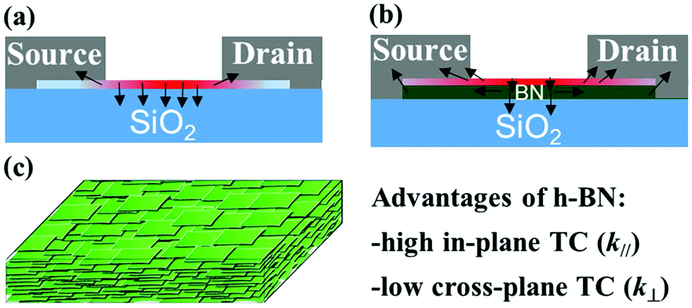 | ||
| Fig. 1 Schematic demonstrating the working principle of an h-BN thin film as an effective thermal management material. Schematic of a heat generating device on (a) a bare glass substrate and on (b) an h-BN thin film coated glass substrate. (c) Schematic of an h-BN thin film comprising layer-by-layer laminated h-BN nanosheets. | ||
The h-BN is thermally conductive and electrically insulating, making it an ideal substrate. However, large-scale preparation of single crystal h-BN is difficult and expensive, and the formed h-BN substrate is incompatible with industrial fabrication.46 An h-BN thin film coated on a substrate, as shown in Fig. 1b, could greatly enhance the lateral heat spreading and reduce the occurrence of hot spots on the substrate.41,42,47
Fig. 1c shows a schematic of the h-BN thin film comprising thousands of layer-by-layer laminated h-BN nanosheets. The h-BN thin film is expected to have a high in-plane thermal conductivity because of the intrinsically high in-plane thermal conductivity of the h-BN nanosheets; meanwhile, the h-BN thin film is also expected to have a low cross-plane thermal conductivity because of the layered structure of the h-BN nanosheets bonded by weak van der Waals force. The low cross-plane thermal conductivity of the h-BN thin film can further prevent local overheating of the substrate directly underneath the device.
The h-BN nanosheets were produced by sonication-assisted liquid-phase exfoliation of bulk h-BN flakes in powder (left panel in Fig. 2a).40,43,48 Excess h-BN powder flakes at an initial concentration of 3 mg mL−1 were put in isopropyl alcohol (IPA) and sonicated for 10 hours, and then a centrifugation procedure (3000 rpm, 15 min) was performed, yielding a white, dilute, and saturated suspension (h-BN ink) dispersed with h-BN nanosheets (right panel in Fig. 2a). Fig. 2b shows a scanning electron microscopy (SEM) image of individual h-BN powder flakes, which have an average lateral dimension of 50 μm and thickness of 5 μm. During sonication, the bulk h-BN flakes are exfoliated into small pieces and becoming h-BN nanosheets. Fig. 2c shows a transmission electron microscopy (TEM) image of a single h-BN nanosheet. The h-BN nanosheets have an average lateral dimension of 1 μm and thickness of 20 nm. The h-BN thin film was produced by the spray-coating technique45 using an ink of dispersed h-BN nanosheets. Fig. 2d shows a schematic of the spray-coating setup. The h-BN ink was vaporized by a spray gun using N2 as a carrier gas. After the IPA vapor containing h-BN nanosheets reached the pre-heated cover glass, the IPA had evaporated and the h-BN nanosheets adhered to the cover glass to form the coated h-BN thin film. The thickness of the h-BN thin film can be controlled by adjusting the spray-coating time and/or the concentration of the h-BN ink. Fig. 2e shows an optical image of the cover glass partially coated with the h-BN thin film (∼300 nm thickness). The h-BN thin film is white, and the region of the cover glass covered by the h-BN thin film becomes less transparent. Fig. 2f shows a top-view SEM image of the h-BN thin film, where the h-BN nanosheets are randomly oriented in the plane and stacked together to form a laminated layer-by-layer structure.
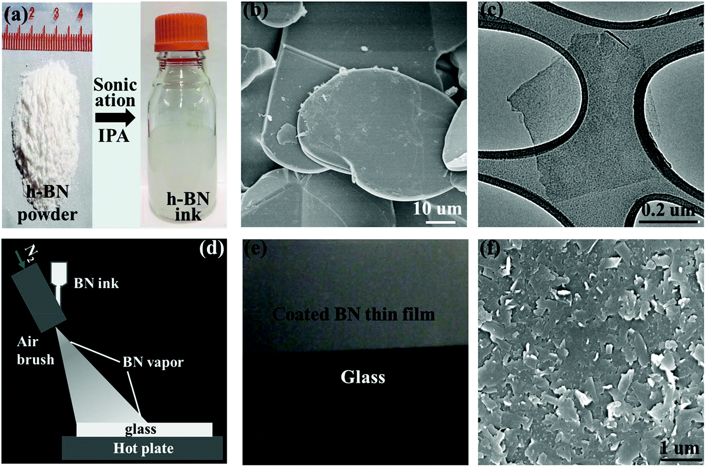 | ||
| Fig. 2 The preparation and characterization of h-BN nanosheets and h-BN thin film. (a) Sonication-assisted liquid-phase exfoliation of bulk h-BN powder flakes to produce h-BN nanosheets, yielding a white, dilute saturated suspension (h-BN ink). (b) SEM image of the individual h-BN powder flakes. (c) TEM image of a single h-BN nanosheet. The h-BN nanosheets have an average lateral dimension of 1 μm and thickness of 20 nm. (d) Schematic of a spray-coating setup to produce the h-BN thin film on the cover glass. (e) Optical image of the cover glass partially covered with the h-BN thin film (∼300 nm). (f) Top-view SEM image of the surface of the h-BN thin film. The h-BN nanosheets are randomly oriented in the plane and stacked together to form the laminated layer-by-layer structure. | ||
Improved thermal management with h-BN thin film coated substrate
To demonstrate the thermal management capabilities of the h-BN thin film, two identical devices based on a reduced graphene oxide (RGO) thin film were fabricated, one on Glass and another on BN/Glass, for comparison. Fig. 3a shows an optical image of the electronic device, where source and drain electrodes are made of silver paste. First, a graphene oxide (GO) thin film (50 nm) was prepared on each substrate by using the same spray-coating technique with a GO dispersion prepared by an improved Hummer's method.49 The insulating GO thin film was then thermally reduced at 300 °C in vacuum to remove the oxygen-containing functional groups, leading to a conductive reduced graphene oxide (RGO) thin film.50 The RGO device is used herein as an example of high power devices due to its high operating temperature.51,52 When the RGO device is in operation, current passes through the RGO thin film. According to the Joule's law, heat generated by a conductor at given current and time can be expressed as: Q = I2 × R × t. Fig. 3b shows an optical image of the RGO device at an operating temperature of ∼650 °C, where the RGO device shines red light at such a high temperature. The RGO device on Glass suddenly fails at an operating temperature of ∼700 °C. Fig. 3c shows an optical image of the failed RGO device on Glass, where the RGO device is broken. The Glass underneath the RGO thin film melted and cracked near the RGO thin film. This is consistent with the fact that glass usually melts at a temperature of >600 °C. The occurrence of cracks in Glass indicates the existence of hot spots in the regions of Glass underneath the RGO device. Because of the breakdown of the Glass substrate, the RGO device failed at ∼700 °C.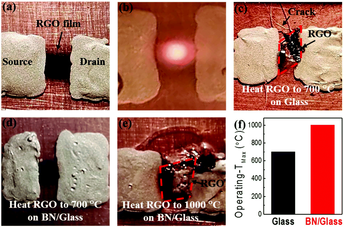 | ||
| Fig. 3 Comparison of the thermal management performances of Glass and BN/Glass using an RGO thin film based device. (a) An optical image of the RGO device on Glass. (b) An optical image of the RGO device heated to ∼650 °C. (c) An optical image of the failed RGO device on Glass after heating to ∼700 °C. The glass substrate underneath the RGO device is melt and cracked. (d) An optical image of the RGO device on BN/Glass after heating to ∼700 °C and holding for 30 minutes. (e) An optical image of the RGO device on BN/Glass after heating to 1000 °C. The underneath glass is melted and the melting region extends to a greater area than the Glass sample. (f) Comparison of the highest operating temperatures for RGO devices on Glass and BN/Glass. | ||
The RGO device on BN/Glass was tested in the same way. Fig. 3d shows an optical image of the RGO device on BN/Glass after testing at ∼700 °C and holding for 30 minutes, where no obvious damage was observed. These results indicate that the BN/Glass substrate can support the power device stably, with normal operation at ∼700 °C. As the input power continuously increases, the RGO device on BN/Glass reaches an operating temperature as high as 1000 °C before it fails. Fig. 3e shows an optical image of the failed RGO device on BN/Glass, where the glass underneath the h-BN thin film melted. The melted region extends out farther than that of Glass shown in Fig. 3c, indicating the effect of the high in-plane thermal conductivity of the h-BN thin film. Fig. 3f shows that the highest operating temperature of the RGO device on BN/Glass increases by 300 °C compared to that of the RGO device on Glass. Details of the device characteristics can be found in Fig. S1.† The improved performance is attributed to the high in-plane and low cross-plane thermal conductivities of the h-BN thin film. The high in-plane thermal conductivity is helpful for spreading the heat away from the device, while the low cross-plane thermal conductivity reduces the heat loading to the glass substrate underneath the RGO device, together preventing the crack and melting of the glass.
To directly compare the heat dissipation performance of the Glass and the BN/Glass substrates, thermographs were captured by FLIR T450sc infrared camera. The RGO devices on Glass and BN/Glass are used as local heat sources. Fig. 4a shows the temperature distributions on Glass and BN/Glass while keeping a maximum temperature of ∼450 °C at the center for both devices. The temperature distribution profile of Glass is narrower than that of the BN/Glass, indicating more effective heat spreading in BN/Glass. Furthermore, the local temperatures of the RGO devices on Glass and BN/Glass at the equal input power were also measured by the infrared camera, as shown in Fig. 4b. With lower input power, no obvious maximum temperature difference was observed for the RGO devices on Glass and BN/Glass; both of them exhibit local maximum temperature lower than 350 °C. As the input power to the RGO devices increases, the maximum local temperature of the RGO device on BN/Glass is always lower than that of the RGO device on Glass. For example, with an input power of 2.5 W to the RGO devices, the maximum local temperatures of the RGO devices on Glass and BN/Glass are 649.3 °C and 574 °C, respectively, indicating the heat dispassion performance of the substrate could be effectively improved by coating an h-BN thin film.
 | ||
| Fig. 4 Comparison of temperature gradient distribution and power dependent temperature for the RGO devices on Glass and BN/Glass. (a) Temperature gradient distribution profiles of the RGO devices on Glass and BN/Glass while keeping a maximum local temperature of ∼450 °C. The temperature gradient of BN/Glass is wider compared to that of Glass. (b) Relationship between input power and maximum local temperatures of the RGO devices on Glass and BN/Glass. At the same input power, the maximum local temperature of the RGO device on BN/Glass is lower than that of the RGO device on Glass. | ||
In-plane and cross-plane thermal conductivities of h-BN thin film
The improved thermal performance of the BN/Glass is due to the high in-plane thermal conductivity and the low cross-plane thermal conductivity of the h-BN thin film. A time-domain thermoreflectance (TDTR)39 with a variable laser spot size approach was used to measure both the in-plane and the cross-plane thermal conductivities of the h-BN thin film. A schematic of our TDTR setup is shown in Fig. 5a. More details on the experimental setup and the sample preparation for TDTR measurements are presented in the Experimental section. The TDTR signal is predominantly sensitive to the cross-plane thermal conductivity when using a large laser spot size for the measurement, where the heat flow is mainly one-dimensional along the cross-plane direction. On the other hand, the TDTR signal is sensitive to both the cross-plane and the in-plane thermal conductivities when using a tightly focused laser spot for the measurement, where the heat flow becomes three-dimensional.39,53 Thus, both the cross-plane and the in-plane thermal conductivities of the h-BN thin film can be determined by conducting two sets of measurements using different laser spot sizes (Fig. 5b). As shown in Fig. 5c, the in-plane and cross-plane thermal conductivities of the h-BN thin film are fitted to be k∥ = 14 ± 5 W m−1 K−1 and k⊥ = 0.4 ± 0.15 W m−1 K−1, respectively. The in-plane thermal conductivity of the h-BN thin film is much higher compared to the thermal conductivity of bare glass, which is k = 1.3 ± 0.2 W m−1 K−1, while the cross-plane thermal conductivity of the h-BN thin film is lower than bare glass. The in-plane thermal conductivity of h-BN film is much smaller than that of single piece of few layer h-BN nanosheets, and can be further improved by increasing the lateral size of h-BN nanosheets laminated in the h-BN film. The thicker h-BN film thickness better benefits the thermal management performance, as evidenced by a simulation shown in Fig. S2.† | ||
| Fig. 5 Anisotropic thermal conductivity of the h-BN thin film. (a) A schematic of the experimental setup (TDTR) and the sample geometry for thermal conductivity measurements of the h-BN thin film. (b) TDTR experimental data on the h-BN thin film (symbols) along with the fittings from a thermal model (solid, red lines) and 30% bounds on the fitted values of the cross-plane (dash, blue lines) and the in-plane (dash-dot, green lines) thermal conductivities, measured using different laser spot sizes. (c) Comparison of the in-plane and cross-plane thermal conductivities of the h-BN thin film and that of the glass. | ||
Conclusion
We demonstrated that a coated BN thin film effectively improves the thermal management capability of the substrate. Comparing the operation of RGO devices on BN/Glass and Glass, the operating temperature of the RGO device on BN/Glass is much lower than that of the RGO device on Glass at the same input power, and the maximum operating temperature of the RGO device on BN/Glass is increased from 700 °C (for RGO device on Glass) to 1000 °C. The improved performance of the BN/Glass is due to the high in-plane (k∥ = 14 ± 5 W m−1 K−1) and the low cross-plane (k⊥ = 0.4 ± 0.15 W m−1 K−1) thermal conductivities of the BN thin film, which leads to fast heat dispassion along the BN surface and helps to block the heat transfer to the substrate directly underneath the device. This work not only provides an effective approach to resolving heat dispassion issues in integrated circuits and high power density devices, but is also helpful for other thermal management applications.Experimental section
Operation of the RGO device on Glass and BN/Glass
The power was applied to the RGO device using a Keithley 2400 SourceMeter at a constant current mode. The operating temperature of the RGO device was measured by a fiber-coupled spectrometer (Ocean Optics. Inc.), which records the emission spectrum. The spectrum was fitted to Planck's law of black-body radiation: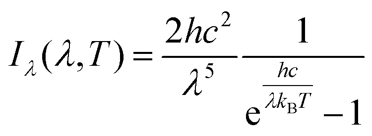 , where I(ν, T) is the measured intensity; h, c, kB, λ and T are the Planck constant, speed of light in a vacuum, Boltzmann constant, wavelength, and absolute temperature, respectively. The measured spectrum fits well with the Planck's law.
Temperature and temperature distribution measurement by the infrared camera
For the temperature distribution profile measurement using an infrared camera, both the RGO devices and the infrared camera were placed in an Ar glove box to avoid infrared absorption of glass if the infrared camera is placed outside the glove box. The FLIR T450sc infrared camera has a spectral range between 7.5–13 μm with a resolution of 320 × 240 pixels.Thermal conductivity measurements
The thermal conductivity of the h-BN film was measured by time-domain thermoreflectance (TDTR) at room temperature. In this method, a Ti:sapphire laser generates a train of femtosecond laser pulses at a repetition rate of 81 MHz with a wavelength centered at 785 nm. The laser output is split into a high-energy pump beam and a low-energy probe beam using a polarized beam splitter. The pump beam is further modulated at a frequency between 0.5 to 10 MHz using an electro-optic modulator (EOM) and then directed onto the sample to induce a small heating event. The probe beam is delayed temporally with respect to the pump via a 600 mm-long mechanical delay stage and then directed onto the sample to interrogate the surface temperature change as a function of the delay time. The measured data were compared to a thermal model calculation, from which we extracted the unknown thermal conductivities of the substrate.To prepare the samples for TDTR measurements, we first deposited a 100 nm-thick Al film on a smooth glass slide, followed by a ∼5-μm-thick h-BN film spray coated on the Al film. We then performed the pump–probe experiments from the glass side. The 5 μm-thick h-BN film could be considered as bulk in our TDTR measurements, as the thermal penetration depth in h-BN in the cross-plane direction, which is defined as 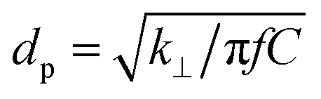 , with f the modulation frequency and C the volumetric heat capacity, is only in the range of 90–400 nm in our experiments, much shorter than the film thickness. The 100 nm-thick Al film serves as a transducer for the TDTR experiments. By depositing the transducer film on a smooth glass slide instead of directly on the rough h-BN film, we can achieve a smooth surface for the transducer that enables specular reflection of the probe beam, which is critical for TDTR measurements.
Author contributions
L. H. and Y. W. designed the experiments; Y. W., L.X., H.X., Z.Y., W.L., and Y.Y. performed the experiments, P.J. and R.Y. performed thermal conductivity measurement; Y.W., L.X., Z.Y., P.J., and L.H. analyzed the data; Y.W., P.J., J.D., and L.H. prepared the manuscript draft while all authors contributed to editing the manuscript.Conflicts of interest
The authors declare no conflict of interest.Acknowledgements
Dr Hu acknowledges the financial support from the Office of Naval Research Young Investigator Program (ONR YIP, Program Manager: Sarwat Chappell). We acknowledge the support of the Maryland NanoCenter, its Surface Analysis Center and AIMLab. Dr Yang acknowledge the financial support from National Science Foundation (Grant # 1512776).References
- I. Ferain, C. A. Colinge and J.-P. Colinge, Nature, 2011, 479, 310–316 CrossRef CAS PubMed.
- E. Pop, S. Sinha and K. E. Goodson, Proc. IEEE, 2006, 94, 1587–1601 CrossRef CAS.
- A. L. Moore and L. Shi, Mater. Today, 2014, 17, 163–174 CrossRef CAS.
- E. Pop and K. E. Goodson, J. Electron. Packag., 2006, 128, 102–108 CrossRef CAS.
- S. V. Garimella, A. S. Fleischer, J. Y. Murthy, A. Keshavarzi, R. Prasher, C. Patel, S. H. Bhavnani, R. Venkatasubramanian, R. Mahajan, Y. Joshi, B. Sammakia, B. A. Myers, L. Chorosinski, M. Baelmans, P. Sathyamurthy and P. E. Raad, IEEE Trans. Compon. Packag. Technol., 2008, 31, 801–815 CrossRef.
- A. A. Balandin, IEEE Spectrum., 2009, 46, 34–39 CrossRef.
- D. G. Cahill and R. O. Pohl, Phys. Rev. B: Condens. Matter Mater. Phys., 1987, 35, 4067–4073 CrossRef CAS.
- T. R. Anthony, W. F. Banholzer, J. F. Fleischer, L. Wei, P. K. Kuo, R. L. Thomas and R. W. Pryor, Phys. Rev. B: Condens. Matter Mater. Phys., 1990, 42, 1104–1111 CrossRef CAS.
- L. Wei, P. K. Kuo, R. L. Thomas, T. R. Anthony and W. F. Banholzer, Phys. Rev. Lett., 1993, 70, 3764–3767 CrossRef CAS PubMed.
- M. Xu, T. Liang, M. Shi and H. Chen, Chem. Rev., 2013, 113, 3766–3798 CrossRef CAS PubMed.
- Y. Wang, N. Xu, D. Li and J. Zhu, Adv. Funct. Mater., 2017, 27, 1604134 CrossRef.
- K. Choi, Y. T. Lee and S. Im, Nano Today, 2016, 11, 626–643 CrossRef CAS.
- J. Shen, Y. Zhu, H. Jiang and C. Li, Nano Today, 2016, 11, 483–520 CrossRef CAS.
- A. Pakdel, C. Zhi, Y. Bando and D. Golberg, Mater. Today, 2012, 15, 256–265 CrossRef CAS.
- Y. Lin and J. W. Connell, Nanoscale, 2012, 4, 6908–6939 RSC.
- A. A. Balandin, Nat. Mater., 2011, 10, 569–581 CrossRef CAS PubMed.
- M. J. Meziani, W.-L. Song, P. Wang, F. Lu, Z. Hou, A. Anderson, H. Maimaiti and Y.-P. Sun, ChemPhysChem, 2015, 16, 1339–1346 CrossRef CAS PubMed.
- C. Zhi, Y. Bando, C. Tang, H. Kuwahara and D. Golberg, Adv. Mater., 2009, 21, 2889–2893 CrossRef CAS.
- J. Wang, V. K. Kayastha, Y. K. Yap, Z. Fan, J. G. Lu, Z. Pan, I. N. Ivanov, A. A. Puretzky and D. B. Geohegan, Nano Lett., 2005, 5, 2528–2532 CrossRef CAS PubMed.
- D.-H. Lien, J. S. Kang, M. Amani, K. Chen, M. Tosun, H.-P. Wang, T. Roy, M. S. Eggleston, M. C. Wu, M. Dubey, S.-C. Lee, J.-H. He and A. Javey, Nano Lett., 2015, 15, 1356–1361 CrossRef CAS PubMed.
- Y. Zhang, L. Zhang and C. Zhou, Acc. Chem. Res., 2013, 46, 2329–2339 CrossRef CAS PubMed.
- Z. Yan, L. Chen, M. Yoon and S. Kumar, Nanoscale, 2016, 8, 4037–4046 RSC.
- A. A. Balandin, S. Ghosh, W. Bao, I. Calizo, D. Teweldebrhan, F. Miao and C. N. Lau, Nano Lett., 2008, 8, 902–907 CrossRef CAS PubMed.
- S. Ghosh, I. Calizo, D. Teweldebrhan, E. P. Pokatilov, D. L. Nika, A. A. Balandin, W. Bao, F. Miao and C. N. Lau, Appl. Phys. Lett., 2008, 92, 151911 CrossRef.
- S. Chen, A. L. Moore, W. Cai, J. W. Suk, J. An, C. Mishra, C. Amos, C. W. Magnuson, J. Kang, L. Shi and R. S. Ruoff, ACS Nano, 2011, 5, 321–328 CrossRef CAS PubMed.
- C. Faugeras, B. Faugeras, M. Orlita, M. Potemski, R. R. Nair and A. K. Geim, ACS Nano, 2010, 4, 1889–1892 CrossRef CAS PubMed.
- J.-U. Lee, D. Yoon, H. Kim, S. W. Lee and H. Cheong, Phys. Rev. B: Condens. Matter Mater. Phys., 2011, 83, 081419 CrossRef.
- W. Cai, A. L. Moore, Y. Zhu, X. Li, S. Chen, L. Shi and R. S. Ruoff, Nano Lett., 2010, 10, 1645–1651 CrossRef CAS PubMed.
- X. Gu and R. Yang, Annu. Rev. Heat Transfer, 2016, 19, 1–65 Search PubMed.
- N. Alem, R. Erni, C. Kisielowski, M. D. Rossell, W. Gannett and A. Zettl, Phys. Rev. B: Condens. Matter Mater. Phys., 2009, 80, 155425 CrossRef.
- D. Golberg, Y. Bando, Y. Huang, T. Terao, M. Mitome, C. Tang and C. Zhi, ACS Nano, 2010, 4, 2979–2993 CrossRef CAS PubMed.
- K. Watanabe, T. Taniguchi and H. Kanda, Nat. Mater., 2004, 3, 404–409 CrossRef CAS PubMed.
- J. Wu, B. Wang, Y. Wei, R. Yang and M. Dresselhaus, Mater. Res. Lett., 2013, 1, 200–206 CrossRef CAS.
- O. Tao, C. Yuanping, X. Yuee, Y. Kaike, B. Zhigang and Z. Jianxin, Nanotechnology, 2010, 21, 245701 CrossRef PubMed.
- E. K. Sichel, R. E. Miller, M. S. Abrahams and C. J. Buiocchi, Phys. Rev. B: Solid State, 1976, 13, 4607–4611 CrossRef CAS.
- I. Jo, M. T. Pettes, J. Kim, K. Watanabe, T. Taniguchi, Z. Yao and L. Shi, Nano Lett., 2013, 13, 550–554 CrossRef CAS PubMed.
- M. T. Alam, M. S. Bresnehan, J. A. Robinson and M. A. Haque, Appl. Phys. Lett., 2014, 104, 013113 CrossRef.
- H. Zhou, J. Zhu, Z. Liu, Z. Yan, X. Fan, J. Lin, G. Wang, Q. Yan, T. Yu, P. M. Ajayan and J. M. Tour, Nano Res., 2014, 7, 1232–1240 CrossRef CAS.
- P. Jiang, X. Qian and R. Yang, Rev. Sci. Instrum., 2017, 88, 074901 CrossRef PubMed.
- J.-C. Zheng, L. Zhang, A. V. Kretinin, S. V. Morozov, Y. B. Wang, T. Wang, X. Li, F. Ren, J. Zhang, C.-Y. Lu, J.-C. Chen, M. Lu, H.-Q. Wang, A. K. Geim and K. S. Novoselov, 2D Mater., 2016, 3, 011004 CrossRef.
- Z. Lin, C. Liu and Y. Chai, 2D Mater., 2016, 3, 041009 CrossRef.
- L. Fu, T. Wang, J. Yu, W. Dai, H. Sun, Z. Liu, R. Sun, N. Jiang, A. Yu and C.-T. Lin, 2D Mater., 2017, 4, 025047 CrossRef.
- H. Zhu, Y. Li, Z. Fang, J. Xu, F. Cao, J. Wan, C. Preston, B. Yang and L. Hu, ACS Nano, 2014, 8, 3606–3613 CrossRef CAS PubMed.
- Z. Zeng, T. Sun, J. Zhu, X. Huang, Z. Yin, G. Lu, Z. Fan, Q. Yan, H. H. Hng and H. Zhang, Angew. Chem., Int. Ed., 2012, 51, 9052–9056 CrossRef CAS PubMed.
- A. Moridi, S. M. Hassani-Gangaraj, M. Guagliano and M. Dao, Surf. Eng., 2014, 30, 369–U329 CrossRef CAS.
- G. Lu, T. Wu, Q. Yuan, H. Wang, H. Wang, F. Ding, X. Xie and M. Jiang, Nat. Commun., 2015, 6, 6160 CrossRef CAS PubMed.
- J. Bao, K. Jeppson, M. Edwards, Y. Fu, L. Ye, X. Lu and J. Liu, Electron. Mater. Lett., 2016, 12, 1–16 CrossRef CAS.
- J. N. Coleman, M. Lotya, A. O'Neill, S. D. Bergin, P. J. King, U. Khan, K. Young, A. Gaucher, S. De, R. J. Smith, I. V. Shvets, S. K. Arora, G. Stanton, H.-Y. Kim, K. Lee, G. T. Kim, G. S. Duesberg, T. Hallam, J. J. Boland, J. J. Wang, J. F. Donegan, J. C. Grunlan, G. Moriarty, A. Shmeliov, R. J. Nicholls, J. M. Perkins, E. M. Grieveson, K. Theuwissen, D. W. McComb, P. D. Nellist and V. Nicolosi, Science, 2011, 331, 568–571 CrossRef CAS PubMed.
- D. C. Marcano, D. V. Kosynkin, J. M. Berlin, A. Sinitskii, Z. Sun, A. Slesarev, L. B. Alemany, W. Lu and J. M. Tour, ACS Nano, 2010, 4, 4806–4814 CrossRef CAS PubMed.
- S. Pei and H.-M. Cheng, Carbon, 2012, 50, 3210–3228 CrossRef CAS.
- Y. Chen, K. Fu, S. Zhu, W. Luo, Y. Wang, Y. Li, E. Hitz, Y. Yao, J. Dai, J. Wan, V. A. Danner, T. Li and L. Hu, Nano Lett., 2016, 16, 3616–3623 CrossRef CAS PubMed.
- W. Bao, A. D. Pickel, Q. Zhang, Y. Chen, Y. Yao, J. Wan, K. Fu, Y. Wang, J. Dai, H. Zhu, D. Drew, M. Fuhrer, C. Dames and L. Hu, Adv. Mater., 2016, 28, 4684–4691 CrossRef CAS PubMed.
- A. J. Schmidt, X. Chen and G. Chen, Rev. Sci. Instrum., 2008, 79, 114902 CrossRef PubMed.
Footnotes |
| † Electronic supplementary information (ESI) available. See DOI: 10.1039/c7nr07058f |
| ‡ These authors contributed equally to this work. |
| This journal is © The Royal Society of Chemistry 2018 |