
 Open Access Article
 This Open Access Article is licensed under a
 Creative Commons Attribution 3.0 Unported Licence
Nanoscale, conformal films of graphitic carbon nitride deposited at room temperature: a method for construction of heterojunction devices†
Satyam A.
Ladva
a,
William
Travis
a,
Raul
Quesada-Cabrera
 a,
Martin
Rosillo-Lopez
a,
Abdulkareem
Afandi
b,
Yaomin
Li
a,
Richard B.
Jackman
b,
Joseph C.
Bear
a,
Ivan P.
Parkin
a,
Christopher
Blackman
a,
Christoph G.
Salzmann
a and
Robert G.
Palgrave
*a
a,
Martin
Rosillo-Lopez
a,
Abdulkareem
Afandi
b,
Yaomin
Li
a,
Richard B.
Jackman
b,
Joseph C.
Bear
a,
Ivan P.
Parkin
a,
Christopher
Blackman
a,
Christoph G.
Salzmann
a and
Robert G.
Palgrave
*a
aDepartment of Chemistry, University College London, London, UK. E-mail: r.palgrave@ucl.ac.uk
bLondon Centre for Nanotechnology and the Department of Electronic and Electrical Engineering, University College London, London, UK
First published on 17th October 2017
Abstract
Graphitic carbon nitrides (GCNs) represent a family of 2D materials composed of carbon and nitrogen with variable amounts of hydrogen, used in a wide variety of applications. We report a method of room temperature thin film deposition which allows ordered GCN layers to be deposited on a very wide variety of substrates, including conductive glass, flexible plastics, nanoparticles and nano-structured surfaces, where they form a highly conformal coating on the nanoscale. Film thicknesses of below 20 nm are achievable. In this way we construct functional nanoscale heterojunctions between TiO2 nanoparticles and GCN, capable of producing H2 photocatalytically under visible light irradiation. The films are hydrogen rich, have a band gap around 1.7 eV, display transmission electron microscopy lattice fringes as well as X-ray diffraction peaks despite being deposited at room temperature, and show characteristic Raman and IR bands. We use cluster etching to reveal the chemical environments of C and N in GCN using X-ray photoelectron spectroscopy. We elucidate the mechanism of this deposition, which operates via sequential surface adsorption and reaction analogous to atomic layer deposition. The mechanism may have implications for current models of carbon nitride formation.
Introduction
Graphitic carbon nitrides (GCNs) are a family of two-dimensional materials similar to graphene or graphite but possessing a band gap of over 1 eV, and have potential applications in a number of fields, including solar energy harvesting,1–6 electrocatalysis,7–9 lithium or sodium ion battery electrodes,10 fuel cells,11 electrochemical actuators12 and sensors.13 Although carbon nitrides are amongst the oldest known polymeric materials, much work remains both to fully characterise their structures and bonding, which is essential to design of functional materials,1,14 and to develop chemical methods to integrate them into devices.15 Recently, ionothermal synthesis has proven a useful route to well defined, oriented graphitic GCN flakes,16,17 and two dimensional GCN sheets have been dissolved into solvents such as aqueous H2SO4, ethanol or DMSO.18,19 Films of GCN have been deposited by a wide variety of techniques, such as magnetron sputtering,20 pulsed laser deposition,21 chemical vapour deposition,22 liquid phase deposition23 and sol–gel processes.24 Here, we report a method of room temperature thin film deposition which allows crystalline GCN layers to be deposited on a very wide variety of substrates, including conductive glass, flexible plastics, nanoparticles and nano-structured surfaces, where they form a highly conformal coating on the nanoscale. We elucidate the mechanism of this deposition, which operates via sequential surface adsorption and reaction analogous to atomic layer deposition. The mechanism may have implications for current models of carbon nitride formation. Films were found to consist of C, N, H, with traces (<0.5 atomic%) of oxygen, were conformal on the nanoscale, and when coated on TiO2 particles were photoactive for visible light sacrificial hydrogen production from an ethanol aqueous solution.Experimental methods
A precursor mixture of dicyandiamide (DCDA), 1.0 g, lithium bromide 0.78 g and potassium bromide 0.72 g was placed in a 10 mm outer diameter quartz tube, sealed at one end, and dried under dynamic vacuum (10−2 mbar) for 20 hours at 180 °C. The tube was back filled with dry nitrogen and vacuum purged three times. The reaction mixture was heated to 600 °C at a rate of 20 °C min−1. The resulting vapours were allowed to enter a coating chamber, which itself had been vacuum purged and nitrogen flushed, and which was kept at room temperature. No carrier gas was used; an oil bubbler allowed overpressure of gas to escape the apparatus whilst excluding air. Substrates placed within the coating chamber became coated with a dark film of an increasing thickness over a period of 30 min–60 hours (ESI, Fig. S1†). Planar substrates (quartz, indium tin oxide coated glass, flexible plastic) nanopowders (TiO2, Al2O3) and nanostructured materials (WO3 nanorods) were coated in this fashion. In fact we have not yet found a substrate upon which a film could not be grown using this method. Further experimental details and characterisation methods are given in the ESI.†Results and discussion
Fig. 1 shows examples of the coated substrates, including photographs of GCN coated flexible acetate plastic and borosilicate glass, and scanning electron microscopy (SEM) images of uncoated and coated WO3 nanorod films.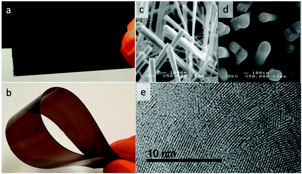 | ||
| Fig. 1 (a) GCN film deposited on glass. (b) GCN film deposited on acetate plastic. (c) SEM image of uncoated WO3 nanorods. (d) SEM image of WO3 nanorods coated with GCN (e) TEM image of GCN film coated directly onto a holey carbon grid, showing lattice fringes. | ||
The film growth rate on planar substrates was measured by masking a part of the substrate before growth and measuring the step edge in the resulting film using a profilometer. This revealed an induction period of approximately 30 min after the reaction mixture attained 600 °C where no film was deposited. Subsequently, the film thickness was linear with deposition time up to 4 hours, with a constant growth rate of 41 nm per hour during this period.
Powder X-ray diffraction (XRD) taken in Bragg–Brentano geometry from the planar thin film samples showed one peak with a d-spacing of 3.25 Å corresponding to the characteristic interplane spacing of GCN,25 and smaller than that seen in graphite.26 HRTEM images taken from GCN films deposited directly onto holey carbon TEM grids at room temperature (Fig. 1e and S2†) showed clear lattice fringes, with d-spacing of 3.0 Å, somewhat smaller than the interlayer spacing seen in XRD, which may indicate that in few-layer assemblies, the interlayer spacing is reduced compared with bulk GCN. Energy dispersive X-ray (EDS) analysis was carried out concurrently with TEM imaging. Only C, N and Cu (from the TEM grid) were detected above 0.5 atomic% (Fig. S3†). O, Li, K, Br were not detected at any level, indicating that the components of the ionic salt do not become incorporated into the deposited films, and that the level of oxidation was low. The C![[thin space (1/6-em)]](https://www.rsc.org/images/entities/char_2009.gif) :N ratio was 1.2. CHN analysis was carried out on the sample, yielding atomic C:N:H ratio of 1.2:1:1.4, indicating a large amount of hydrogen present in the sample, as well as confirming the C/N ratio found by TEM EDS.
:N ratio was 1.2. CHN analysis was carried out on the sample, yielding atomic C:N:H ratio of 1.2:1:1.4, indicating a large amount of hydrogen present in the sample, as well as confirming the C/N ratio found by TEM EDS.
To complement the TEM, EDS and CHN analysis, XPS was used to determine the sample surface composition and chemical environments present. A GCN film was grown on borosilicate glass coated with TiO2 as a barrier layer to prevent ion migration from the glass. For the as-synthesised samples, the surface of the material consisted of C and N, with small amounts of O and Si also detected (Fig. S6†). No Ti was detected indicating complete coverage of the underlying substrate, and no Br, K or Li were detected indicating that those components of the reaction mixture are not incorporated into the film within the detection limits of XPS. The C 1s peak at the surface could be fitted with components at 284.6 eV, 286.7 eV and 289.0 eV (Fig. 2). The 284.6 eV environment corresponds to graphitic carbon, and is typically seen in XPS due to surface environmental contamination. This peak may conceivably originate from the GCN structure itself, and thus it is important to be able to distinguish between surface environmental contamination and carbon environments within GCN. However, in situ monoatomic Ar ion cleaning, used to remove surface contamination, is known to damage GCN and lead to significant changes in chemistry and composition.27,28 Hence XPS characterisation of GCN materials is challenging, as it has been difficult to reliably remove surface contamination without changing the chemical nature of the GCN itself, and so unambiguous assignments of the carbon environments observed in XPS has not been possible. To overcome this, we used Ar cluster ion etching. Ar cluster ion etching for 60 s resulted in removal of Si to below the detection limit of the instrument (c. 0.1 atomic%), reduction of the oxygen content to below 2.0 atomic%, and very significant reduction in the C 1s component at 284.6 eV. The C/N ratio after 60 s of cleaning was 1.00, slightly lower than that recorded by both TEM EDS and CHN analysis, although XPS is known to be less accurate for absolute compositions. Successive cluster etching cycles up to 570 s caused no change in the C/N ratio, and no further change to the C 1s peak, indicating that the cluster etching avoids the problems associated with monoatomic Ar ion etching. Therefore, after removal of surface graphitic carbon contamination, the C 1s spectrum consisted of a peak at 286.7 eV with a small component at 289.0 eV, while the N 1s peak could be fitted with a single Gaussian–Lorentzian peak shape centred at 399.6 eV. These peak positions are consistent with those seen in GCN samples produced by a variety of methods.15
 | ||
| Fig. 2 X-ray photoelectron spectra of the C 1s region of GCN film on glass. Data was fitted with three Gaussian–Lorentzian components as described in the text. Etching using monoatomic or clusters of Ar ions was used in an attempt to remove the graphitic carbon contamination. Spectra taken after various etching times using the different sources are shown. Mono Ar etching causes significant changes to the spectrum with extended etching, whereas cluster Ar etching does not. | ||
Raman spectra revealed an asymmetric peak between 1200 and 1750 cm−1 (Fig. S5†); this feature is commonly seen in carbon nitride and related materials produced in a wide variety of ways,29–31 and analogously to the vibrations seen in graphite, is assigned to the G and D vibrations of the carbon nitride structure. Such broad Raman peaks are seen in even highly crystalline samples.29 The ID/IG ratio was 0.51 and the position of the G peak was 1561 cm−1. The intensity of the D peak has been related to the proportion of tetrahedrally bonded (sp3) carbon, and the ratio observed here matches carbon nitride films with high nitrogen contents (>30 atomic%),30,32 consistent with the XPS, CHN and EDS compositions reported above.
Infrared spectra showed three bands associated with the carbon nitride structure (Fig. S5†). A weak, broad feature around 3200 cm−1 is typical of N–H or O–H stretching modes;32 the low intensity of this feature compared to the other absorption bands indicates that the oxygen content is low, in agreement with the XPS and TEM EDS results. A peak at 2170 cm−1 is assigned to nitrile groups. The broad peak at around 1600 cm−1 is characteristic of carbon nitride materials but this assignment remains controversial. Whilst this feature coincides with the Raman signal discussed above, the origin of the IR absorption is assigned to extended conjugated system.32,33 The substrate (glass) has strong absorption bands in the 1000–500 cm−1 region. Although this region is thus partially obscured, there is no evidence of a triazine breathing mode around 800 cm−1.
UV/vis transmission spectra showed broad absorption across the visible region (Fig. S5†). The direct band gap calculated using a Tauc plot was 1.73 eV, consistent with previous measurements of GCN materials produced ionothermally,17 although this value is smaller than many other reported GCN band gaps.25
The identity of the gas phase products of the ionothermal reaction which act to deposit conformal carbon nitride films was studied using time-resolved mass spectrometry (Fig. 3). 10 mg of the reaction mixture (DCDA, KBr, LiBr) was placed in a tube furnace attached to a RC RGA Analyser mass spectrometer. The sample was heated to 600 °C under the same conditions as used in film deposition. Upon heating between 180 °C and 400 °C, two peaks at m/z ratios of 17 and 18 were detected and assigned to NH3 and H2O respectively. At ∼400 °C, the pressure of NH3 begins to decline and the two more intense peaks appear at m/z ratios of 27 and 42 which are assigned to HCN and CN2H2 (likely to be cyanamide) respectively; all three species are expected decomposition products of DCDA. At the same time H–79Br and H–81Br at m/z values of 80 and 82 respectively were detected, indicating some degree of reaction of the salt mixture, however, analyses reported above indicate that Br is not incorporated into the films despite its presence in the gas phase. CH2N2 and HCN reached their maximum pressures at 400 °C and 600 °C, respectively. Thus upon heating, the reaction mixture produced first NH3, then CH2N2 and finally HCN. HCN is known to polymerise in the presence of NH3, which acts as a catalyst, forming solid HCN polymers; this reaction is thought to be important in the origin of life.34,35 We propose that in our apparatus (Fig. S1†), NH3, being first produced from the reaction mixture, adsorbs onto the substrate, then when exposed to gas phase HCN, a polymerisation reaction occurs on the surface, catalysed by the adsorbed NH3, forming a solid product with composition close to HCN. It is possible that CH2N2 also plays a role that is yet to be elucidated. Hence the deposition acts in a similar way to atomic layer deposition (ALD),36 in which precursors are dosed sequentially onto a substrate to effect conformal coating.
 | ||
| Fig. 3 (a) Time resolved gas phase mass spectrometry showing the species produced by the reaction mixture over time. The partial pressures of three key species: NH3, HCN, CH2N2 are shown. (b) Film thickness of GCN film with deposition time, showing an initial induction period where no film is grown, followed by a linear growth rate. (c) Proposed mechanism of sequential absorption and reaction of the gas phase precursors, leading to polymerisation of HCN to form a hydrogen rich GCN material. | ||
To further study the deposition process, deposition of GCN on WO3 nanorods (produced by a CVD technique reported previously37) was carried out, and led to conformal coating of the nanorods with a GCN film. Fig. 1d shows SEM images of nanorods before and after deposition. It is clear that the coating is conformal on the nanoscale; this conformality supports the hypothesis that this process acts via a pseudo-ALD mechanism, which is known to give highly conformal coatings.
Our analyses indicate that we deposit a hydrogen rich GCN material with composition close to C1N1H1. The layered structure, observed by XRD and TEM matches that reported for a variety of GCN structures and demonstrates the graphitic nature of the material. The lack of a triazine peak in the IR or XRD analyses suggests that the structure is not predominantly triazine based. The presence of nitrile groups is suggested by IR spectroscopy. XPS shows one principle carbon environment at 286.7 eV binding energy, indicative of carbon bound to nitrogen, with minimal aliphatic carbon expected around 285 eV. Additionally only one nitrogen environment is seen. Together with the proposed gas phase formation mechanism, i.e. polymerisation from HCN and NH3, we propose our material is a layered polymer of HCN with disordered structure within the layers.
Since the discovery of GCN as a metal-free photocatalyst for the production of hydrogen under visible light illumination,38 there has been a fast-increasing interest on these materials for energy applications.39–43
Our GCN coating when immobilised on Al2O3 powder or on glass did not show visible light photocatalytic water splitting activity in our initial tests, but when coated onto a standard commercial TiO2 powder (Evonik P25) we found that hydrogen was produced from a sacrificial aqueous solution under visible light (Fig. S9†). Details of these experiments are provided in ESI.† Formation of hydrogen ([H2] rate = 1.85 × 10⁻² μmol h−1 g−1) was confirmed upon visible-light (λ > 420 nm) irradiation of a platinised TiO2/Pt-gCN dispersion within 18 h. No detectable H2 was produced by platinised TiO2 alone, in the absence of GCN coating. This suggests a sensitisation or charge transfer process across the GCN/TiO2 heterojunction, and highlights the possibility of producing such nanoscale heterojunction devices using this method.
Conclusion
We have developed a vapour phase method to deposit ordered, layered, graphitic carbon nitride materials on virtually any substrate. The films are conformal on the nanoscale and appear to be deposited via a pseudo-ALD process whereby sequential adsorption and reaction of NH3 and HCN yield hydrogen rich polymeric species. This mechanism is in contrast to previously suggested mechanisms, whereby cyanamide or dicyandiamide reacts to form melamine, which polymerises eventually to form GCN,8,44 or alternatively GCN can be made by thermal treatment of polymers.45 The mechanism outlined here may represent an important alternative pathway for the synthesis of GCN materials, highlighting a new route to applications of GCN in devices where thin films are required, such as battery application, photocatalysts and fuel cells.Author contributions
RGP, SL and WT conceived and designed the experiments. SL and WT carried out the GCN deposition experiments. IPP and RQC conceived and carried out photocatalysis measurements. MRL and CGS carried out gas phase mass spectrometry measurements. RBJ and AA carried out profilometry measurements. JCB conducted coating of TEM grids and carried out TEM measurements. YL and CSB grew WO3 nanorods and carried out electron microscopy studies thereof. RGP and SL wrote the manuscript. All authors commented on the manuscript.Conflicts of interest
There are no conflicts to declare.Acknowledgements
SL and RGP acknowledge funding from Thermo Fisher Scientific and EPSRC though the UCL M3S CDT (EP/L015862/1). RQC and IPP would like to thank Dr Chris Clarke and Aleksandrs Sergejevs for assembling the LEDs board as part of their activities in the PCATDES project (EU N. 309846). JCB acknowledges the Ramsay Memorial Trust for a fellowship. Y. L. thanks the China Scholarship Council (CSC File No. 201406370157) for funding, and the UCL Dean's prize for a joint Ph.D. scholarship.References
- K. Schwinghammer, B. Tuffy, M. B. Mesch, E. Wirnhier, C. Martineau, F. Taulelle, W. Schnick, J. Senker and B. V. Lotsch, Angew. Chem., Int. Ed., 2013, 52, 2435–2439 CrossRef CAS PubMed.
- J. Li, G. M. Zhan, Y. Yu and L. Z. Zhang, Nat. Commun., 2016, 7, 11480 CrossRef CAS PubMed.
- J. Liu, Y. Liu, N. Liu, Y. Han, X. Zhang, H. Huang, Y. Lifshitz, S.-T. Lee, J. Zhong and Z. Kang, Science, 2015, 347, 970–974 CrossRef CAS PubMed.
- X. Wang, K. Maeda, A. Thomas, K. Takanabe, G. Xin, J. M. Carlsson, K. Domen and M. Antonietti, Nat. Mater., 2009, 8, 76–80 CrossRef CAS PubMed.
- Z. W. Zhao, Y. J. Sun and F. Dong, Nanoscale, 2015, 7, 15–37 RSC.
- Y. W. Zhang, J. H. Liu, G. Wu and W. Chen, Nanoscale, 2012, 4, 5300–5303 RSC.
- Y. Zheng, Y. Jiao, Y. H. Zhu, L. H. Li, Y. Han, Y. Chen, A. J. Du, M. Jaroniec and S. Z. Qiao, Nat. Commun., 2014, 5, 3783 Search PubMed.
- F. K. Kessler, Y. Zheng, D. Schwarz, C. Merschjann, W. Schnick, X. Wang and M. J. Bojdys, Nat. Rev. Mater., 2017, 2, 17030 CrossRef CAS.
- J. Q. Tian, Q. Liu, C. J. Ge, Z. C. Xing, A. M. Asiri, A. O. Al-Youbi and X. P. Sun, Nanoscale, 2013, 5, 8921–8924 RSC.
- T. S. Miller, A. B. Jorge, A. Sella, F. Cora, P. R. Shearing, D. J. L. Brett and P. F. McMillan, Electroanalysis, 2015, 27, 2614–2619 CrossRef CAS.
- Y. Zheng, J. Liu, J. Liang, M. Jaroniec and S. Z. Qiao, Energy Environ. Sci., 2012, 5, 6717–6731 CAS.
- G. Wu, Y. Hu, Y. Liu, J. J. Zhao, X. L. Chen, V. Whoehling, C. Plesse, G. T. M. Nguyen, F. Vidal and W. Chen, Nat. Commun., 2015, 6, 7258 CrossRef CAS PubMed.
- S. W. Zhang, J. X. Li, M. Y. Zeng, J. Z. Xu, X. K. Wang and W. P. Hu, Nanoscale, 2014, 6, 4157–4162 RSC.
- V. W. H. Lau, I. Moudrakovski, T. Botari, S. Weinberger, M. B. Mesch, V. Duppel, J. Senker, V. Blum and B. V. Lotsch, Nat. Commun., 2016, 7, 12165 CrossRef CAS PubMed.
- T. Miller, A. B. Jorge, T. Suter, A. Sella, F. Cora and P. McMillan, Phys. Chem. Chem. Phys., 2017, 19, 15613–15638 RSC.
- M. J. Bojdys, J. O. Muller, M. Antonietti and A. Thomas, Chem. – Eur. J., 2008, 14, 8177–8182 CrossRef CAS PubMed.
- G. Algara-Siller, N. Severin, S. Y. Chong, T. Bjorkman, R. G. Palgrave, A. Laybourn, M. Antonietti, Y. Z. Khimyak, A. V. Krasheninnikov, J. P. Rabe, U. Kaiser, A. I. Cooper, A. Thomas and M. J. Bojdys, Angew. Chem., Int. Ed., 2014, 53, 7450–7455 CrossRef CAS PubMed.
- Z. X. Zhou, J. H. Wang, J. C. Yu, Y. F. Shen, Y. Li, A. R. Liu, S. Q. Liu and Y. J. Zhang, J. Am. Chem. Soc., 2015, 137, 2179–2182 CrossRef CAS PubMed.
- T. S. Miller, T. M. Suter, A. M. Telford, L. Picco, O. D. Payton, F. Russell-Pavier, P. L. Cullen, A. Sella, M. S. P. Shaffer, J. Nelson, V. Tileli, P. F. McMillan and C. A. Howard, Nano Lett., 2017, 17, 5891–5896 CrossRef CAS PubMed.
- H. Sjostrom, L. Hultman, J. E. Sundgren, S. V. Hainsworth, T. F. Page and G. Theunissen, J. Vac. Sci. Technol., A, 1996, 14, 56–62 Search PubMed.
- D. Fischer, K. Schwinghammer, C. Sondermann, V. W. Lau, J. Mannhart and B. V. Lotsch, Appl. Surf. Sci., 2015, 349, 353–360 CrossRef CAS.
- Y. G. Wang, F. Wang, Y. H. Zuo, X. D. Zhang and L. F. Cui, Mater. Lett., 2014, 136, 271–273 CrossRef CAS.
- J. S. Xu, T. J. K. Brenner, L. Chabanne, D. Neher, M. Antonietti and M. Shalom, J. Am. Chem. Soc., 2014, 136, 13486–13489 CrossRef CAS PubMed.
- J. S. Zhang, M. W. Zhang, L. H. Lin and X. C. Wang, Angew. Chem., Int. Ed., 2015, 54, 6297–6301 CrossRef CAS PubMed.
- J. J. Zhu, P. Xiao, H. L. Li and S. A. C. Carabineiro, ACS Appl. Mater. Interfaces, 2014, 6, 16449–16465 CAS.
- P. Trucano and R. Chen, Nature, 1975, 258, 136–137 CrossRef CAS.
- S. Bhattacharyya, C. Cardinaud and G. Turban, J. Appl. Phys., 1998, 83, 4491–4500 CrossRef CAS.
- C. Ronning, H. Feldermann, R. Merk, H. Hofsass, P. Reinke and J. U. Thiele, Phys. Rev. B: Condens. Matter, 1998, 58, 2207–2215 CrossRef CAS.
- P. F. McMillan, V. Lees, E. Quirico, G. Montagnac, A. Sella, B. Reynard, P. Simon, E. Bailey, M. Deifallah and F. Cora, J. Solid State Chem., 2009, 182, 2670–2677 CrossRef CAS.
- A. C. Ferrari, S. E. Rodil and J. Robertson, Diamond Relat. Mater., 2003, 12, 905–910 CrossRef CAS.
- M. Y. Chen, D. Li, X. Lin, V. P. Dravid, Y. W. Chung, M. S. Wong and W. D. Sproul, J. Vac. Sci. Technol., A, 1993, 11, 521–524 CAS.
- S. E. Rodil, A. C. Ferrari, J. Robertson and S. Muhl, Thin Solid Films, 2002, 420, 122–131 CrossRef.
- A. C. Ferrari, S. E. Rodil and J. Robertson, Phys. Rev. B: Condens. Matter, 2003, 67, 155306 CrossRef.
- C. U. Lowe, R. Markham and M. W. Rees, Nature, 1963, 199, 219–222 CrossRef CAS PubMed.
- C. N. Matthews and R. D. Minard, Faraday Discuss., 2006, 133, 393–401 RSC.
- S. M. George, Chem. Rev., 2010, 110, 111–131 CrossRef CAS PubMed.
- M. Ling, C. S. Blackman, R. G. Palgrave, C. Sotelo-Vazquez, A. Kafizas and I. P. Parkin, Adv. Mater. Interfaces, 2017, 1700064, DOI:10.1002/admi.201700064.
- X. Wang, S. Blechert and M. Antonietti, ACS Catal., 2012, 2, 1596–1606 CrossRef CAS.
- L. H. Lin, H. H. Ou, Y. F. Zhang and X. C. Wang, ACS Catal., 2016, 6, 3921–3931 CrossRef CAS.
- H. H. Ou, P. J. Yang, L. H. Lin, M. Anpo and X. C. Wang, Angew. Chem., Int. Ed., 2017, 56, 10905–10910 CrossRef CAS PubMed.
- L. H. Lin, C. Wang, W. Ren, H. H. Ou, Y. F. Zhang and X. C. Wang, Chem. Sci., 2017, 8, 5506–5511 RSC.
- A. Savateev, S. Pronkin, J. D. Epping, M. G. Willinger, C. Wolff, D. Neher, M. Antonietti and D. Dontsova, ChemCatChem, 2017, 9, 167–174 CrossRef CAS.
- G. Zhang, G. Li, Z.-A. Lan, L. Lin, A. Savateev, T. Heil, S. Zafeiratos, X. Wang and M. Antonietti, Angew. Chem., Int. Ed., 2017, 56, 13445–13449 CrossRef CAS PubMed.
- B. V. Lotsch and W. Schnick, Chem. – Eur. J., 2007, 13, 4956–4968 CrossRef CAS PubMed.
- A. Savateev, S. Pronkin, J. D. Epping, M. G. Willinger, M. Antonietti and D. Dontsova, J. Mater. Chem. A, 2017, 5, 8394–8401 CAS.
Footnote |
| † Electronic supplementary information (ESI) available. See DOI: 10.1039/c7nr06489f |
| This journal is © The Royal Society of Chemistry 2017 |