
 Open Access Article
 This Open Access Article is licensed under a Creative Commons Attribution-Non Commercial 3.0 Unported Licence
From electroburning to sublimation: substrate and environmental effects in the electrical breakdown process of monolayer graphene†
Maria
El Abbassi‡
 *ab,
László
Pósa‡
c,
Péter
Makk
a,
Cornelia
Nef
a,
Kishan
Thodkar
ab,
András
Halbritter
c and
Michel
Calame
abd
*ab,
László
Pósa‡
c,
Péter
Makk
a,
Cornelia
Nef
a,
Kishan
Thodkar
ab,
András
Halbritter
c and
Michel
Calame
abd
aDepartment of Physics, University of Basel, Klingelbergstrasse 82, CH-4056 Basel, Switzerland. E-mail: maria.elabbassi@unibas.ch
bEmpa, Swiss Federal Laboratories for Materials Science and Technology, Transport at Nanoscale Interfaces Laboratory, CH-8600 Dubendorf, Switzerland
cDepartment of Physics, Budapest University of Technology and Economics and MTA-BME Condensed Matter Research Group, Budafoki ut 8, 1111 Budapest, Hungary
dSwiss Nanoscience Institute, University of Basel, 4056 Basel, Switzerland
First published on 5th October 2017
Abstract
We report on the characterization of the electrical breakdown (EB) process for the formation of tunneling nanogaps in single-layer graphene. In particular, we investigated the role of oxygen in the breakdown process by varying the environmental conditions (vacuum and ambient conditions). We show that the density of oxygen molecules in the chamber is a crucial parameter that defines the physical breakdown process: at low density, the graphene lattice is sublimating, whereas at high density, the process involved is oxidation, independent of the substrate material. To estimate the activation energies of the two processes, we use a scheme which consists of applying voltage pulses across the junction during the breakdown. By systematically varying the voltage pulse length, and estimating the junction temperature from a 1D thermal model, we extract activation energies which are consistent with the sublimation of graphene under high vacuum and the electroburning process under air. Our study demonstrates that, in our system, a better control of the gap formation is achieved in the sublimation regime.
Control of the molecule–electrode interface remains one of the main challenges in the field of molecular electronics. As variations in the molecular-junction geometry have a huge impact on the charge transport properties,1–3 establishing a way to reliably form nanometer-sized gaps is a crucial step towards the realization of reproducible molecular devices with well-defined contact geometries. Another key aspect is the electrode material, which critically determines the binding process4 and junction stability.5,6 Graphene, by its unique properties, is a good candidate to address this problem as it offers a flat and gateable platform with new binding possibilities. Another key benefit is the high structural stability, even at room temperature.7
The use of graphene as an electrode material has been demonstrated experimentally,8–10 and relies on the formation of nanogaps using the electroburning process.8,9,11 In a previous study, we have reported on the fabrication of such nanogaps with sizes down to a few nanometers using an optimized electrical breakdown (EB) protocol. Even though we achieved a junction formation yield of >95%,12 the details of the EB process itself are still not fully understood. Here, in order to identify the key parameters in the EB process, we study the influence of the environmental conditions, and in particular, the role of the oxygen content. We find that under ambient conditions, the EB is caused by the conventional electroburning process, while under high vacuum, sublimation takes place. By using a simple heat-transport model, we extract estimates for the relevant activation energies, which are consistent with the proposed electroburning and sublimation processes. To exclude the substrate as a source of oxygen, we also performed a comparative study of the EB process on SiO2 and Si3N4 substrates. In contrast to previous reports,13 we find that the presence of oxygen in the substrate does not play a role in the EB process.
Graphene structures are fabricated using chemical vapor deposited (CVD) graphene grown on Cu foil. The selected CVD growth process produces single layer graphene with a typical grain size of 10 μm.14 The graphene is transferred using a wet etching method15 to two different substrates: doped silicon substrate coated with either 300 nm of thermal oxide (Si/SiO2), or 80 nm thermal oxide and 140 nm of Si3N4 (Si/SiO2/Si3N4). The graphene is first patterned into narrow bridges (400 nm wide and 800 nm long) using standard e-beam lithography and oxygen plasma etching and then contacted with Ti/Au (5/55 nm) deposited by e-beam evaporation. The schematic of our samples is shown in the inset of Fig. 1a.
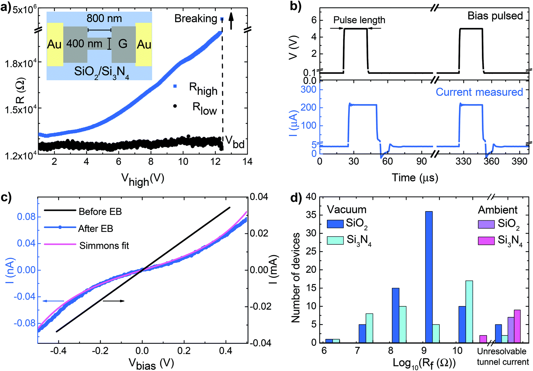 | ||
| Fig. 1 Description of the EB process: (a) Resistance at high bias Rhigh (in blue) and low bias Rlow (in black) during the EB of a device under vacuum with pulse lengths of 10 ms. An increase of resistance due to Joule heating is observed at high bias. At breakdown voltage Vbd, a jump of resistance is observed, as a sign of the gap formation. The inset is a schematic of the device. (b) The applied voltage pulse is shown with the simultaneously recorded current for a pulse length of 25 μs. (c) Current–voltage characteristic of a device before and after EB. Before EB, the I–V curve is linear and the current is in the mA range (right axis, black). After EB, we measure non-linear I–V curves with currents in the nA range due to the presence of a gap (left axis, blue). The pink curve represents a Simmons fit of the tunneling curve. (d) Distribution of the low bias resistance Rf at zero gate voltage of the junctions after EB under vacuum and under ambient conditions for both substrates. For resistances larger than 1011 Ω, no tunnel current could be resolved. | ||
Nanogaps were formed using the EB of the graphene bridges. The EB process was performed by high voltage pulses with increasing amplitude. The current response was measured for each pulse (Fig. 1b), from which the high bias resistance was calculated (Rhigh). At each EB step, the pulse height, Vhigh, was increased by 5 mV, and the process was stopped after the first pulse, when Rhigh exceeded 500 kΩ. This often corresponds to a jump in the resistance. The influence of the pulse length on the EB process was systematically studied using 5 μs to 5 s pulses. Between subsequent pulses, an offset voltage of 100 mV was applied to determine the low bias resistance, Rlow. The measurements were performed both under ambient conditions (under air) and under high vacuum (down to p = 10−7 mbar).
Fig. 1a shows the evolution of Rhigh and Rlow for a typical EB process under vacuum with a pulse length of 10 ms. Due to Joule heating,16Rhigh increases as the pulse height is increased, whereas Rlow remains almost constant until the breakdown occurs at Vbd. Changes of the low bias resistance can occur because of annealing effects. Different polymer residues from the transfer and lithography resist can lead to a change of the graphene resistance due to increased scattering or doping effects. The high current during EB induces cleaning of the devices and hence changes of the resistance.17
Fig. 1c shows the I–V curves of a graphene bridge before and after EB. Before EB, the current–voltage characteristic of the graphene bridge is linear with a resistance of 12.5 kΩ. After EB, the device shows S-shaped I–V curves, characteristic for tunneling. Assuming a rectangular barrier, we can fit the curves to the Simmons model18 and obtain an estimate of the gap size of about 1.5 nm for this particular device. The details of the fitting process and the distribution of the fitted gap sizes can be found in the ESI† and in ref. 12. The low bias resistance of the graphene nanogaps after EB provides a first indication about the size and the cleanliness of the gap. It has been suggested that an ideal device should have a resistance of a few GΩ.19 Very wide gaps will exhibit larger resistance values, often resulting in unresolvable tunnel currents. Lower resistances, in the MΩ regime, can be explained by the presence of carbon islands or residues bridging the gap. To test the latter, we have systematically performed gate dependent measurements of the tunneling behavior at room temperature. A few devices were also characterized at low temperature (see the ESI†). The majority of the devices, typically more than 70%, do not show any gate dependence at room temperature. Fig. 1d shows the distribution of the low bias resistances after EB for SiO2 and Si3N4 substrates both under vacuum and under air at zero gate voltage.
In our measurements the EB always happens immediately: even if we apply ultrashort pulses (down to 5 μs width), we cannot detect any precursor of the breakdown before the last, breaking pulse. In agreement with our previous report12 on SiO2 substrates, here we observed that for both substrates a measurable tunnel current corresponding to a few nm gap size is achieved with a yield of 95% if the EB is performed under vacuum (see the gap size distribution in the ESI†). Under air, however, there is a much higher chance to achieve unmeasurably large resistance values, and thus a large and uncontrolled gap size. We note that in ref. 8, 11, 19 and 23, gradual breakdown and smaller gap sizes are achieved under air using real time feedback controlled EB protocol with >200 μs response time, and different sample geometries (e.g. multilayer exfoliated graphene8,23 and single-layer CVD graphene with a bow-tie geometry11,19,20). It is not yet clarified whether this different behavior can be attributed to fabrication differences or distinct driving protocols.
The EB of graphene is commonly attributed to an electroburning process:8,9 due to the current induced high local temperature, the graphene atoms oxidize at the hottest point of the junction and form a nanogap. Under high vacuum, however, a much smaller number of oxygen molecules are available and other processes may take place, similarly as in the study of carbon nanotubes,21 where electroburning is replaced with oxide failure/sublimation as the pressure is decreased. To study this effect, we performed EB measurements both under air and under high vacuum. In addition to the pressure, we also varied the length of the voltage pulses.
For all pulse lengths, an average power was calculated from measurements on 2 to 5 devices on Si3N4 and SiO2 substrates (Fig. 2a, small symbols) under ambient conditions and under vacuum (p = 10−7 mbar). The figures clearly show that for both substrates, a higher power is needed for the breakdown under vacuum than under air. We also notice that on average, a higher power is required to break a junction on a SiO2 substrate than on Si3N4. A larger number of devices were measured under vacuum with 10 ms pulse length for both substrates. The corresponding distribution of breakdown power is shown in Fig. 2b. An average value and a standard deviation are extracted from the data using a Gaussian fit. The values of the fit parameters are plotted in the left panel (bigger symbols with error bars representing the standard deviation). We can notice that the values extracted from the measurements of a higher number of devices are in a good agreement with the trend observed during the change of the pulse length.
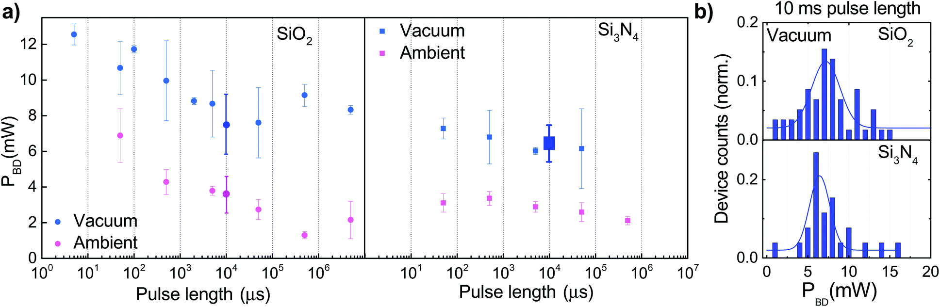 | ||
| Fig. 2 (a) Average breakdown power for graphene nanostructures on SiO2 (left) and on Si3N4 (right) as a function of pulse length under vacuum (blue) and under ambient conditions (pink). An average breakdown power is calculated from the measurements of 2 to 5 devices (small symbols). The corresponding distribution is not shown. The error bars represent the standard deviation of these datapoints. (b) Distribution of the breakdown powers for Si3N4 and SiO2 for a pulse length of 10 ms under vacuum. Measurements are reported from 52 devices for SiO2 and 24 devices for Si3N4. The lines correspond to the Gaussian fit of the distribution. As a reference the mean values and the standard deviations of the fitted Gaussians are represented as larger symbol panel (a). Similar measurements were carried out for SiO2 under air (large pink dot). | ||
To study the effect of oxygen from the atmosphere on the EB process, we first estimate the number of oxygen molecules arriving on a single atomic site during the breakdown process. According to the kinetic theory of gases the flux of oxygen molecules from 2π solid angle to the graphene sample is jox = nox![[v with combining macron]](https://www.rsc.org/images/entities/i_char_0076_0304.gif) /4 where nox and are the density and the average speed of the oxygen molecules, respectively. These quantities are defined as nox = αoxp/(kBT), where αox = 0.21 is the fraction of oxygen molecules under air, p is the pressure, T = 300 K is the temperature and kB is the Boltzmann constant. The average speed of the oxygen molecules is expressed as
/4 where nox and are the density and the average speed of the oxygen molecules, respectively. These quantities are defined as nox = αoxp/(kBT), where αox = 0.21 is the fraction of oxygen molecules under air, p is the pressure, T = 300 K is the temperature and kB is the Boltzmann constant. The average speed of the oxygen molecules is expressed as  , where μ = 5.31 × 10⁻²⁶ kg is the mass of an oxygen molecule. From these, the number of oxygen molecules arriving to a half unit cell of graphene (single atomic site) during a single pulse is N ≈ 1.5 × 10⁷·τ·p/pambient, where τ is the pulse length in seconds and pambient is the atmospheric pressure. Since the carrier cooling time for graphene is in the order of picoseconds,22 we consider the heating/cooling time constant much shorter than our pulse length, i.e. we assume that our graphene bridge is hot only during the pulse. Based on all these, with the pressure (10−7 mbar to 1 bar) and with the pulse length (5 μs to 5 s), we can experimentally tune the number of oxygen molecules hitting an atomic site during a single pulse by 16 orders of magnitude.
To interpret the data in terms of electroburning, it is useful to give a common axis to Fig. 2a showing the number of oxygen molecules hitting an atomic site during a single pulse. This rescaled top axis is shown in Fig. 3, such that the vertical axis is scaled to temperature (see later), and the raw power data with the common top axis are shown in Fig. S1 of the ESI.† Under high vacuum, the number of oxygen molecules/atomic site during the breakdown is much smaller than 1 for any pulse length, indicating that a breakdown process different than burning may take place. One could still speculate that similarly to ref.13 the oxygen from the SiO2 substrate may take part in the burning process even in the absence of atmospheric oxygen; however, the fact that on the Si3N4 substrate a similar EB is observed under vacuum stands against this assumption. In this regime, we rather attribute the breakdown to the sublimation of graphene. In the following, we try to understand the different breakdown processes using a heat transport model.
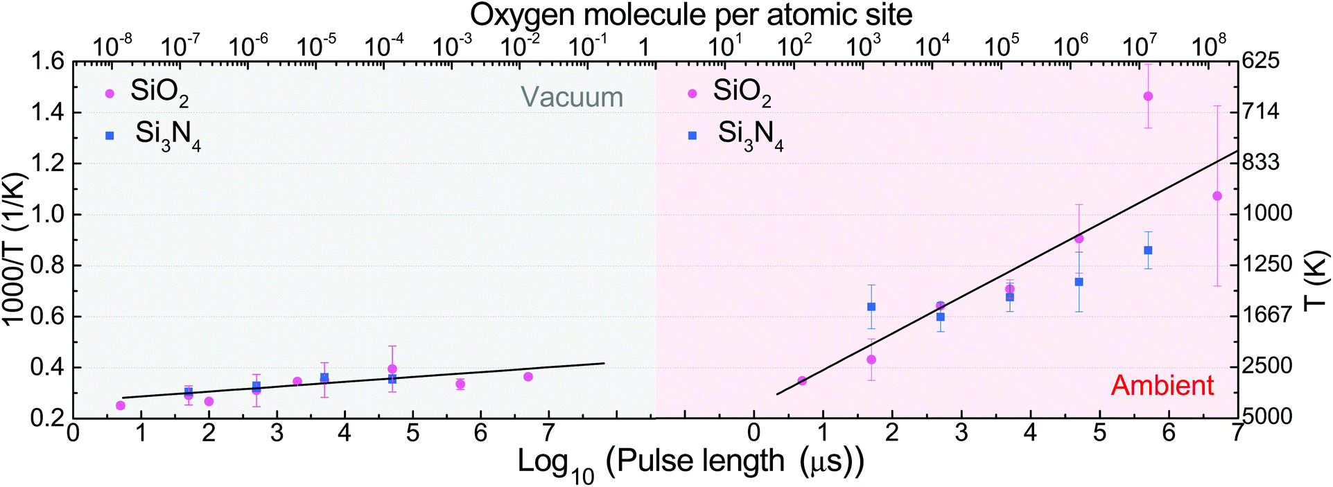 | ||
| Fig. 3 Arrhenius plot of 1/T as a function of the logarithmic pulse length for Si3N4 (in blue) and SiO2 (in pink). The top axis is scaled to the number of oxygen molecules arriving on a single atomic site during a single EB pulse. The right axis shows the maximum temperature within the junction. To estimate the temperature, we fixed the thermal conductivities to κg = 1000 W K−1 m−1, κox = 1.4 W K−1 m−1 and κni = 30 W K−1 m−1, and the thermal boundary resistivity ρgox to 1 × 10⁻⁸ m2 K W−1. To determine the activation energies, two separate lines were fitted to the vacuum and the ambient regions. The thermal boundary resistivity ρgni was tuned to achieve the least squares deviation between the temperatures calculated for Si3N4 and SiO2. This procedure yielded ρgni 4.8 × 10⁻⁷ m2 K W−1. | ||
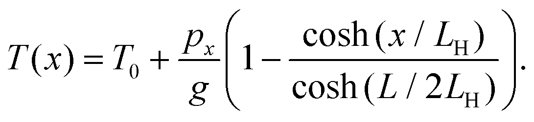
As the EB shows similar tendencies on both substrates, we assume that both on SiO2 and on Si3N4, the same physical processes are involved in the breakdown. This means that at a given pulse length and pressure, the breakdown should happen at the same local temperature of graphene regardless of the chosen substrate. Therefore we wish to rescale the axis of the breakdown power to the maximal local temperature of the graphene junction when the EB happens. To estimate the power dependence of the temperature of the graphene constriction during EB, one can use the analytic solution of the 1D heat equation.23 Assuming that the temperature at the contacts is fixed to room temperature (T0), one obtains:
 | (1) |
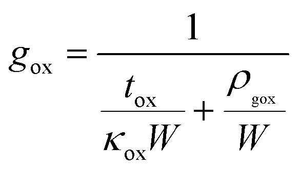
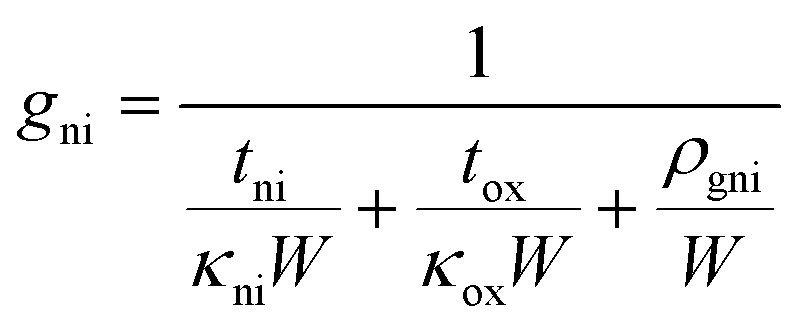
Here L = 800 nm is the length of the constriction, g is the thermal conductance to the substrate per unit length, px is the Joule heating rate in Watts per unit length, and LH is the thermal healing length defined as: 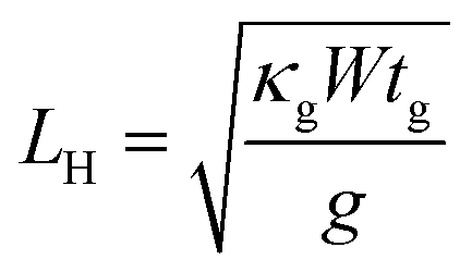 , where tg = 0.335 nm is the thickness of a monolayer of graphene, W = 400 nm is the width of the constriction, and κg is the heat conductivity of graphene. Throughout our calculations we use a constant heat conductivity of κg = 1000 W K−1 m−1, which is consistent with the data from J. O. Island et al.23 For the SiO2 substrate the thermal conductance to the substrate is calculated as:
 | (2) |
 | (3) |
The parameters used for our model are given in the caption of Fig. 3. All the parameters were taken from the literature,23,24 except the thermal boundary resistivity between Si3N4 and graphene, for which we are not aware of any prior measurement. Relying on the assumption that the breakdown should happen at the same temperature using SiO2 or Si3N4, we use ρgni as a fitting parameter to obtain the least squares deviation between the breakdown temperatures on both substrates at the various pulse lengths and pressures. This fitting yields a value of ρgni = 4.8 × 10⁻⁷ m2 K W−1 for the thermal boundary resistivity. Note that this value is more than an order of magnitude larger than the thermal boundary resistivity for SiO2, which indicates weak van der Waals interactions between graphene and the Si3N4 substrate.
As both the electroburning and the sublimation are activated processes, the number of reactions per unit area and unit time can be written as:
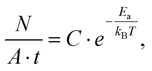 | (4) |
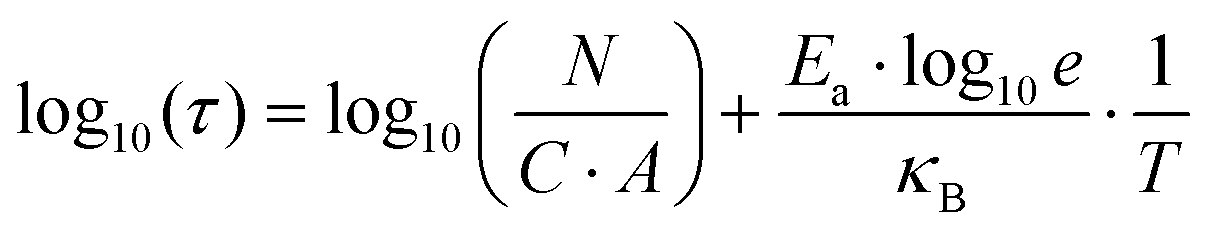 | (5) |
In summary, we have studied the EB process, used for creating graphene nanogaps, under different conditions. We have shown that the process of breakdown is different for low and high oxygen concentrations. At high oxygen concentration a conventional electroburning process takes place. As the pressure is lowered, the system enters a regime where no oxygen molecules can reach the junction during a single voltage pulse. In this regime, the EB process can still take place but at a significantly higher power than under ambient conditions. Based on the systematic study of the breakdown power at various pulse lengths, and the conversion of power to contact temperature using a thermal model, we have estimated the activation energies of the involved processes. According to this analysis the EB process is shown to be consistent with electroburning under ambient conditions and sublimation under high vacuum. By performing a comparative study using SiO2 and Si3N4 substrates, we have also shown that the oxygen originating from SiO2 does not play a substantial role in the breakdown process.
Conflicts of interest
There are no conflicts to declare.Acknowledgements
This work was funded by the NKFIH grants K112918 and K119797 and the EC FP7-ITN MOLESCO grant (no. 606728). This work was partially supported by the Swiss Federal Institute of Metrology (METAS) via the EMRP project GraphOhm (SIB51). The authors thank Mickael Perrin and Anton Vladyka for fruitful discussions and Erwin Hack for carefully reading the manuscript and for his comments.References
- Special issue molecular electronics, Nat. Nanotechnol., 2013, 8, 385–389 CrossRef PubMed.
- J. Ulrich, et al. , J. Phys. Chem. B, 2006, 110, 2462–2466 CrossRef CAS PubMed.
- R. Frisenda, et al. , Phys. Rev. Lett., 2016, 117, 126804 CrossRef CAS PubMed.
- D. Cahen, et al. , Adv. Mater., 2002, 14(11), 789–798 CrossRef CAS.
- F. Prins, et al. , J. Appl. Phys. Lett., 2009, 94, 123108 CrossRef.
- F. Prins, et al. , Phys. Chem. Chem. Phys., 2011, 13, 14297 RSC.
- C. Jia, et al. , Acc. Chem. Res., 2015, 48(9), 2565–2575 CrossRef CAS PubMed.
- F. Prins, et al. , Nano Lett., 2011, 11(11), 4607–4611 CrossRef CAS PubMed.
- J. Mol, et al. , Nanoscale, 2015, 7, 13181 RSC.
- C. Jia, et al. , Science, 2016, 352(6292), 1443–1445 CrossRef CAS PubMed.
- C. S. Lau, et al. , Phys. Chem. Chem. Phys., 2014, 16, 20398–20401 RSC.
- C. Nef, et al. , Nanoscale, 2014, 6, 7249 RSC.
- J. Beilstein, Nanotechnol., 2015, 6, 711–719 Search PubMed.
- K. Thodkar, et al. , Phys. Status Solidi, 2016, 10(11), 807–811 CAS.
- J. W. Suk, et al. , ACS Nano, 2011, 5(9), 6916–6924 CrossRef CAS PubMed.
- L. Grosse, et al. , Nat. Nanotechnol., 2011, 6, 287–290 CrossRef PubMed.
- J. Moser, et al. , Appl. Phys. Lett., 2007, 91, 163513 CrossRef.
- J. G. Simmons, J. Appl. Phys., 1963, 34, 1793 CrossRef.
- P. Gehring, et al. , Nano Lett., 2016, 16(7), 4210–4216 CrossRef CAS PubMed.
- J. O. Island, et al. , J. Phys.: Condens. Matter, 2014, 26, 474205 CrossRef CAS PubMed.
- A. Liao, et al. , Phys. Rev. B, 2010, 82, 205406 CrossRef.
- K. J. Tielrooij, et al. , Nat. Nanotechnol., 2015, 10, 437–443 CrossRef CAS PubMed.
- J. O. Island, et al. , J. Phys.: Condens. Matter, 2014, 26, 474205 CrossRef CAS PubMed.
- A. A. Balandin, Nano Lett., 2008, 8(3), 902–907 CrossRef CAS PubMed.
- J. Y. Huang, et al. , Proc. Natl. Acad. Sci. U. S. A., 2009, 106(25), 10103–10108 CrossRef CAS PubMed.
- A. Santana, et al. , Chem. Phys. Lett., 2013, 557, 80–87 CrossRef CAS.
- A. Barreiro, et al. , Nano Lett., 2012, 12(4), 1873–1878 CrossRef CAS PubMed.
- N. Tao, et al. , J. Phys. Chem. C, 2011, 115(11), 4730–4737 Search PubMed.
Footnotes |
| † Electronic supplementary information (ESI) available: Effect of the thermal transport parameters on the estimated junction temperature and the activation energies are presented together with details on the Simmons fitting procedure and the room/low temperature gate dependence of the I(V) curves after the electrical breakdown. See DOI: 10.1039/C7NR05348G |
| ‡ These authors contributed equally to this work. |
| This journal is © The Royal Society of Chemistry 2017 |