
Alignment control and atomically-scaled heteroepitaxial interface study of GaN nanowires†
 *a
*a
Abstract
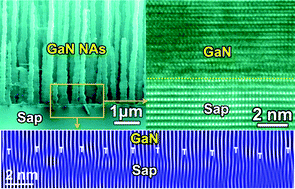
Well-aligned GaN nanowires are promising candidates for building high-performance optoelectronic nanodevices. In this work, we demonstrate the epitaxial growth of well-aligned GaN nanowires on a [0001]-oriented sapphire substrate in a simple catalyst-assisted chemical vapor deposition process and their alignment control. It is found that the ammonia flux plays a key role in dominating the initial nucleation of GaN nanocrystals and their orientation. Typically, significant improvement of the GaN nanowire alignment can be realized at a low NH3 flow rate. X-ray diffraction and cross-sectional scanning electron microscopy studies further verified the preferential orientation of GaN nanowires along the [0001] direction. The growth mechanism of GaN nanowire arrays is also well studied based on cross-sectional high-resolution transmission electron microscopy (HRTEM) characterization and it is observed that GaN nanowires have good epitaxial growth on the sapphire substrate following the crystallographic relationship between (0001)GaN∥(0001)sapphire and (10![[1 with combining macron]](https://www.rsc.org/images/entities/char_0031_0304.gif) 0)GaN∥(11
0)GaN∥(11![[2 with combining macron]](https://www.rsc.org/images/entities/char_0032_0304.gif) 0)sapphire. Most importantly, periodic misfit dislocations are also experimentally observed in the interface region due to the large lattice mismatch between the GaN nanowire and the sapphire substrate, and the formation of such dislocations will favor the release of structural strain in GaN nanowires. HRTEM analysis also finds the existence of “type I” stacking faults and voids inside the GaN nanowires. Optical investigation suggests that the GaN nanowire arrays have strong emission in the UV range, suggesting their crystalline nature and chemical purity. The achievement of aligned GaN nanowires will further promote the wide applications of GaN nanostructures toward diverse high-performance optoelectronic nanodevices including nano-LEDs, photovoltaic cells, photodetectors etc.
0)sapphire. Most importantly, periodic misfit dislocations are also experimentally observed in the interface region due to the large lattice mismatch between the GaN nanowire and the sapphire substrate, and the formation of such dislocations will favor the release of structural strain in GaN nanowires. HRTEM analysis also finds the existence of “type I” stacking faults and voids inside the GaN nanowires. Optical investigation suggests that the GaN nanowire arrays have strong emission in the UV range, suggesting their crystalline nature and chemical purity. The achievement of aligned GaN nanowires will further promote the wide applications of GaN nanostructures toward diverse high-performance optoelectronic nanodevices including nano-LEDs, photovoltaic cells, photodetectors etc.
 Please wait while we load your content...

