Electric field directed self-assembly of block copolymers for rapid formation of large-area complex nanopatterns†
Hyun Uk
Jeon
,
Hyeong Min
Jin
 ,
Ju Young
Kim
,
Seung Keun
Cha
,
Jeong Ho
Mun
,
Kyung Eun
Lee
,
Jung Jae
Oh
,
Taeyeong
Yun
,
Jun Soo
Kim
and
Sang Ouk
Kim
,
Ju Young
Kim
,
Seung Keun
Cha
,
Jeong Ho
Mun
,
Kyung Eun
Lee
,
Jung Jae
Oh
,
Taeyeong
Yun
,
Jun Soo
Kim
and
Sang Ouk
Kim
 *
*
National Creative Research Initiative Center for Multi-Dimensional Directed Nanoscale Assembly, Department of Materials Science and Engineering, KAIST, Daejeon 34141, Republic of Korea. E-mail: sangouk.kim@kaist.ac.kr
First published on 19th September 2017
Abstract
We investigate the unusually rapid directed self-assembly of block copolymer (BCP) thin films by imposing an in-plane electric field. Blending short chain BCPs dramatically enhances the generically retarded chain diffusivity for BCP self-assembly in thin films. In addition, photopatterned, few-layer solution-cast chemically modified graphene is introduced as a disposable and versatile electrode for electric field applications. A variety of laterally ordered self-assembled lamellar BCP nanopatterns are attained within a 10 min time scale, including an arbitrary large-area unidirectionally oriented lamellar array.
Design, System, ApplicationA practical, highly-efficient electric field directed block copolymer self-assembly system is designed. Our key strategy is based on the increase of polymer diffusivity by means of blending short chain polymers as well as the employment of photopatterned chemically modified graphene as a novel electrode for electric field application. The blending ratio of the short chain copolymers is precisely controlled to achieve well-aligned, high-quality nanopatterns. Orientation order parameters of the resultant nanopatterns are presented for quantitative analysis. In addition, we monitor the size of ill-aligned grains over time and confirm that the diffusion barrier is effectively lowered. Taken together, well-aligned nanopatterns can be obtained only within 10 minutes under ambient conditions. Additionally, the chemically modified graphene electrode material enables the inherent problems of metal electrodes to be overcome, such as atomic diffusion and the harsh removal process. Finally, we attain novel nanopatterns including unidirectionally or radially aligned lamellae based on delicately designed electrode structures. |
Introduction
Block copolymer (BCP) self-assembly offers an enormous opportunity for low cost scalable nanopatterning of device oriented structures, including magnetic storage media, membranes, polarizers, semiconductor devices and so on.1–13 Customization of the lateral ordering and the orientation of self-assembled nanodomains in the thin film geometry have been the principal issue in the relevant application fields. To this end, various principles of directed self-assembly (DSA) have been introduced14,15 thus far, most of which utilize chemically or topographically prepatterned substrates. Unfortunately, preparation of the prepatterned structures requires an excessive processing burden for many applications, particularly, other than semiconductors, and practically limits the geometry and material composition for pattern substrates.4–6,16–21Electric fields (E-field) have been extensively utilized to control the molecular orientation of soft matter, such as liquid crystals. The orientation of BCP self-assembled nanodomains is also known to be controllable using an E-field.22–27 Previous studies have successfully identified the underlying mechanism for BCP nanodomain alignment by an E-field.28–31 Local dielectric anisotropy arising from the distinct dielectric properties of chemically different polymer blocks is the principal driving force. E-field alignment is particularly attractive with an expectation for less processing burden, compared to conventional DSA methods that require a delicate substrate pre-patterning process. Unfortunately, the intrinsic low mobility of BCP chains commonly leads to an excessive processing time for a moderate degree of ordering of self-assembled nanopatterns.25,32,33 In addition, conventional metal electrodes limit the application of E-field based DSA, typically aiming at semiconductor device fabrication.
Herein, we present the E-field-driven rapid in-plane alignment of BCP self-assembled nanopatterns employing versatile graphene electrodes. The enhanced chain mobility of BCPs enabled by blending with short copolymers offers highly aligned (orientation order parameter of ∼0.94) lamellar self-assembled morphologies within 10 minutes under conventional thermal annealing with an E-field (25 V μm−1). Noteworthy is that this is the fastest directed self-assembly behavior among those found in the relevant studies employing an in-plane E-field (ESI,† S1). We found that a lowered polymer chain diffusion barrier through the blending with short copolymers34 reduces the critical grain size for the lamellar re-arrangement along the E-field. Noteworthy is that instead of the usual metal electrodes, a chemically modified graphene (CMG) film of a few layers is introduced as a versatile electrode and offers great opportunities for E-field DSA application.2,35–43 The CMG electrode structures can be readily disposed without damaging the BCP films or the semiconductor substrates and are easily patternable into an arbitrary shape by typical photolithography.
Results and discussion
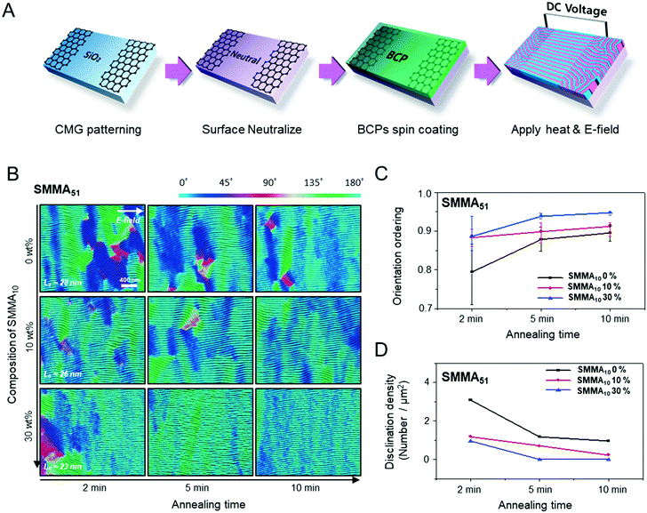
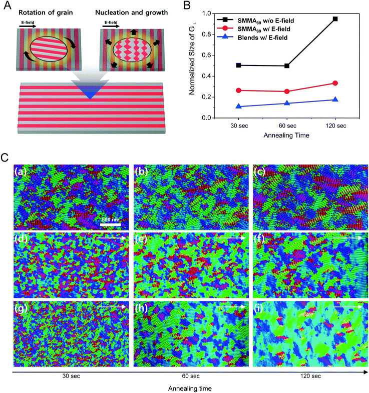
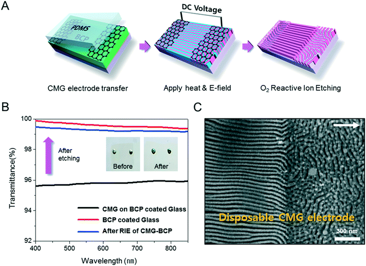
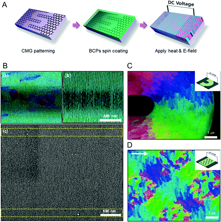
Fig. 1A describes our procedure for the E-field directed self-assembly of BCP thin films. Symmetric lamellar forming polystyrene-block-poly(methyl methacrylate) (SMMA), whose molecular weight (Mn) is 51 kg mol−1 (SMMA51), was principally used in this work. The short chain SMMA, having a Mn of 10 kg mol−1 (SMMA10) was used for the acceleration of E-field assisted DSA via blending with SMMA51 (SMMA51+10). The entire substrate surface, including the patterned CMG electrode surfaces and the gap area between two parallel electrodes, was treated with a neutral polymer brush for the vertical alignment of lamellae. After the spin coating of the BCP thin film (typical thickness: 140–180 nm) over the substrate area, an in-plane direct current (DC) potential (typical field strength: 25 V μm−1) was applied along the in-plane direction simultaneously under thermal annealing at 240 °C. To achieve a well-aligned nanopattern without damage from electrical short and oxidative degradation in air, the E-field strength and annealing time were carefully controlled. Thermal annealing at 240 °C for 150 min under 20 V μm−1 resulted in the completely degraded BCP patterns. A strong E-field over 30 V μm−1 also significantly degrades the polymer thin film morphology within 30 minutes. Eventually, we chose the appropriate E-field strength of 25 V μm−1 and annealing time of less than 90 min in air (Fig. S2†). Finally, the well-aligned lamellar self-assembled structures along the E-field direction were generated. For the rapid E-field assisted DSA, SMMA10 is blended with SMMA51 at various compositions. Time-resolved orientation color maps for the various blending ratios are shown in Fig. 1B. Blending of SMMA10 noticeably accelerates the in-plane lamellar alignment behavior. In particular, 30 wt% SMMA10 blended SMMA51 shows remarkably rapid alignment with minimal defect density typically within 10 minutes (Fig. 1C and D). We found that the nanostructures are collapsed and undulated with a more than 40 wt% SMMA10 blending ratio (Fig. S3†). As shown in Fig. 1C, the orientation order parameter saturates at ∼0.9 in 10 min. Fig. 1D presents the time evolution of defect density, which agrees well with the evolution of the orientation order parameter. In pure SMMA51 BCP films without short copolymer chains, a comparable orientation order parameter is unattainable even after 30 min under the same annealing conditions and E-field strength. Blends of higher molecular weight BCPs with SMMA10 also showed similar tendencies for the accelerated alignment of self-assembled nanopatterns. For a better understanding of the mechanism for E-field DSA, we investigated the nanoscale structural evolution in an early stage of ordering. We observed the alignment behavior of a higher molecular weight BCP, SMMA89, under similar experimental conditions, because SMMA51 is hard to resolve in its early stage of morphological evolution due to its relatively fast structural evolution kinetics. Fig. 2A schematically describes the two possible pathways for BCP alignment via an E-field: “rotation of grains (RG)” and “nucleation and growth (NG)”. For both mechanisms, randomly oriented lamellar grains are nucleated and grow with minor disturbances until the grain size reaches a critical value (Vc). Once a sufficient energy penalty has accumulated in the ill-aligned grain (i.e. V > Vc), the ill-aligned grain starts to re-orient along the E-field direction. The BCP chains become able to overcome the diffusion barrier with the additional energy gained from the E-field. In detail, in the RG mechanism, the chain diffusion along the grain boundary with high defect density is a facile way for re-orientation. Generally, the RG process is dominant in the range of a strong segregation state. Thus, it is possible to re-orient the ill-aligned lamellar grain with minimum chain diffusion (with a high inter-block diffusion barrier). Near the order–disorder transition (ODT), the NG mechanism becomes dominant. The additional energy gain from the E-field makes the ill-aligned grain attain a weak segregation state. As a result, the lamellae undulation is enhanced, from which newly generated well-aligned lamellar grains start to grow without disturbance from the E-field.31,44 The remaining low energy dislocations are annihilated following the typical defect coupling. Owing to the low density of dislocations, elimination of these defects proceeds rather slowly. Fig. 2C shows the time resolved orientation color maps for SMMA89 without an E-field (a–c), SMMA89 under an E-field (d–f) and SMMA89 blended with SMMA10 (SMMA89+10) under an E-field (g–i). The reddish regions indicate ill-aligned lamellar grains, and their average sizes are compared in Fig. 2B. Here, we could see two interesting results for the E-field DSA. First, SMMA89+10 shows a smaller average size of ill-aligned grains than SMMA89, even though there is no structural difference in the initial stage (Fig. S4†). SMMA89+10 has a lower inter-block diffusion barrier due to the lowered effective χN through the blending with neutral small chains (SMMA10). Therefore, the effective VC of SMMA89+10 could be reduced and most of the lamellar grains could be aligned along the E-field in the early stage. More significantly, the bi-axially overlapped lamellar structures are observed (reddish region), which strongly suggests that the NG mechanism should govern the alignment process. Based on the studies of Onuki's group45 and Böker's group,31 the NG mechanism is the more dominant process at the vicinity of the ODT. Under weak segregation between blocks, the E-field can easily induce in-plane undulations or buckling layer instabilities.In the field of semiconductor device fabrication, E-field assisted DSA that requires metallic electrode formation could be hardly considered compatible. The diffusion of metallic atoms can cause the electrical short and disturb the overall performance of semiconductor devices. The acidic removal process of electrodes would be also harsh and may damage the device structures. To address this practical challenge, a CMG electrode is introduced into our E-field assisted DSA which successfully avoids any concern for metal diffusion and electrode removal processes. Fig. 3A presents the E-field DSA with the CMG electrodes, which is dry transferred on the top surface of BCP thin films using a poly(dimethyl siloxane) rubber pad. After the E-field application for nanopattern alignment, the CMG electrodes could be easily removed by a simple O2 reactive ion etching (RIE) process. Fig. 3B shows the optical transmittance before and after the removal of CMG electrodes. Randomly oriented lamellar structures are formed at the right side of Fig. 3C, which were previously covered by the CMG electrode. Underneath the CMG electrode, the direction of the E-field is perpendicular to the substrate, and thus there is no in-plane alignment. Interestingly, the E-field induced lamellar alignment can penetrate into the CMG electrode about 200 nm from the edge of the electrodes. Lamellae tend to maintain their E-field induced alignment for a certain length scale even without any guiding effect in this region. Motivated by this behavior, interdigitated 400 nm width CMG electrodes were devised for large area alignment of vertical lamellar arrays. Fig. 4A illustrates the schematic procedure for the large-area E-field alignment. While randomly oriented fingerprint lamellar patterns were formed in the middle of CMG electrodes wider than 400 nm (Fig. 4B-a), highly aligned lamellar nanopatterns are formed over the entire surface of 400 nm or less width electrodes (Fig. 4B-b). CMG electrodes with a regularly spaced 400 nm width enable highly aligned vertical lamellae over an arbitrary large area (Fig. 4B-c).
As shown in Fig. 4C and D, we also demonstrate various alignment patterns of vertical lamellar arrays, by means of novel designs of CMG electrodes. Fig. 4C shows the orientation map of radially aligned lamellar nanopatterns assembled in the gap area between the curved electrodes. This type of lamellar pattern could be applicable for hyper lens or meta-material fabrication.46Fig. 4D presents a complex orientation of BCP lamellae induced by an array of isolated circular CMG patterns located between two parallel CMG electrodes. The isolated circular CMG patterns are also electrically polarized by the external E-field from neighboring parallel electrodes, and generate a local E-field between the nearest circular CMG patterns. As a consequence, network like nanopatterns are generated, which is hardly attainable by conventional DSA process.
Conclusions
We have demonstrated rapid E-field directed self-assembly of BCPs for large-area diverse nanopattern shapes. Significantly, the CMG electrode, which is readily patternable by conventional photolithography, is successfully introduced as a disposable and transferrable electrode. Owing to the greatly enhanced self-assembly kinetics from blending with short chain BCPs, we firstly demonstrate large-area, rapid, in-plane alignment of self-assembled lamellar structures under a moderate E-field strength of 25 V μm−1. Furthermore, we present novel morphological designs of electrodes and thus attain unprecedented complicated two-dimensional self-assembled nanopatterns. We expect that this new concept of E-field directed BCP self-assembly could be also complementarily integrated with other DSA principles, including graphoepitaxy or epitaxial self-assembly, for more accelerated structure formation and diverse nanopattern shapes.Experimental
Fabrication of CMG electrodes
A graphene oxide (GO) aqueous dispersion was prepared by the modified Hummers method, as described elsewhere. GO films were spin cast on Piranha treated silicon dioxide (SiO2) substrates. Afterwards, thermal reduction was performed under H2 conditions at 600–1000 °C. Noteworthy is that the surface energy of CMG could be precisely tuned by means of reduction temperature and time. I-line photolithography and subsequent O2 RIE was conducted on the CMG film to prepare patterned electrodes. The resultant CMG patterned electrode remaining on the SiO2 substrate could be transferred onto the top surface of BCP thin films with the aid of hydrogen fluoride (HF) vapor etching of the underlying SiO2 layer and a poly(dimethyl siloxane) (PDMS) transfer master.Surface neutralization and BCP nanopatterning
Various molecular weights of symmetric SMMA, such as 10, 51 and 89 kg mol−1, were used in this experiment. For the surface neutralization, hydroxyl terminated poly(styrene-random-methyl methacrylate) solution in toluene having neutral properties for the SMMA lamellae was spin cast on the SiO2 substrate or CMG electrode surface. After thermal treatment at 120–160 °C under vacuum, unreacted neutral random copolymers were removed via toluene rinsing, while a surface-grafted monolayer polymer layer remained. BCP solutions with or without blending with short chain BCPs were spin cast on a target substrate with CMG electrodes. A homemade probe station with the heater at the bottom of the station was used for the thermal annealing of the BCP sample under an E-field. The annealing temperature was ∼240 °C. An electric potential of 20–25 V μm−1 was applied on the CMG electrode via a DC power supply.Measurements
Scanning electron microscopy (SEM) (Hitachi S-4800) was used for imaging the BCP self-assembled nanopatterns. To enhance the contrast of SEM images, PMMA blocks are selectively removed by O2 RIE. Software ImageJ is used for analysis of the SEM images.Conflicts of interest
There are no conflicts to declare.Acknowledgements
This work was financially supported by the Multi-Dimensional Directed Nanoscale Assembly Creative Research Initiative (CRI) Center (2015R1A3A2033061), the Global Frontier Hybrid Interface Materials (GFHIM) through the National Research Foundation of Korea (NRF) funded by the Ministry of Science, ICT and Future Planning (2013M3A6B1078874).Notes and references
- S. J. Jeong, H. S. Moon, B. H. Kim, J. Y. Kim, J. Yu, S. Lee, M. G. Lee, H. Choi and S. O. Kim, ACS Nano, 2010, 4, 5181–5186 CrossRef CAS PubMed.
- B. H. Kim, J. Y. Kim, S. J. Jeong, J. O. Hwang, D. H. Lee, D. O. Shin, S. Y. Choi and S. O. Kim, ACS Nano, 2010, 4, 5464–5470 CrossRef CAS PubMed.
- C. J. Hawker and T. P. Russell, MRS Bull., 2005, 30, 952–966 CrossRef CAS.
- B. H. Kim, J. Y. Kim and S. O. Kim, Soft Matter, 2013, 9, 2780–2786 RSC.
- S. J. Jeong, J. Y. Kim, B. H. Kim, H. S. Moon and S. O. Kim, Mater. Today, 2013, 16, 468–476 CrossRef CAS.
- S. Park, J. M. Yun, U. N. Maiti, H.-S. Moon, H. M. Jin and S. O. Kim, Nanotechnology, 2014, 25, 14008 CrossRef PubMed.
- H. M. Jin, S. H. Lee, J. Y. Kim, S. W. Son, B. H. Kim, H. K. Lee, J. H. Mun, S. K. Cha, J. S. Kim, P. F. Nealey, K. J. Lee and S. O. Kim, ACS Nano, 2016, 10, 3435–3442 CrossRef CAS PubMed.
- M. P. Stoykovich and P. F. Nealey, Mater. Today, 2006, 9, 20–29 CrossRef CAS.
- C. T. Black, Appl. Phys. Lett., 2005, 87, 1–3 CrossRef.
- C. A. Ross, K. K. Berggren, J. Y. Cheng, Y. S. Jung and J. B. Chang, Adv. Mater., 2014, 26, 4386–4396 CrossRef CAS PubMed.
- S. B. Darling, Energy Environ. Sci., 2009, 2, 1266–1273 CAS.
- I. Botiz and S. B. Darling, Macromolecules, 2009, 42, 8211–8217 CrossRef CAS.
- S. Xiong, Y.-A. Chapuis, L. Wan, H. Gao, X. Li, R. Ruiz and P. F. Nealey, Nanotechnology, 2016, 27, 415601 CrossRef PubMed.
- Y. C. Tseng and S. B. Darling, Polymer, 2010, 2, 470–489 CAS.
- S. B. Darling, Prog. Polym. Sci., 2007, 32, 1152–1204 CrossRef CAS.
- S. O. Kim, B. H. Kim, D. Meng, D. O. Shin, C. M. Koo, H. H. Solak and Q. Wang, Adv. Mater., 2007, 19, 3271–3275 CrossRef CAS.
- M. P. Stoykovich, Science, 2005, 308, 1442–1446 CrossRef CAS PubMed.
- S. O. Kim, H. H. Solak, M. P. Stoykovich, N. J. Ferrier, J. J. de Pablo and P. F. Nealey, Nature, 2003, 424, 411–414 CrossRef CAS PubMed.
- B. H. Kim, Y. Choi, J. Y. Kim, H. Shin, S. Kim, S. W. Son, S. O. Kim and P. Kim, Adv. Mater., 2014, 26, 4665–4670 CrossRef CAS PubMed.
- J. Y. Cheng, C. A. Ross, H. I. Smith and E. L. Thomas, Adv. Mater., 2006, 18, 2505–2521 CrossRef CAS.
- E. Sivaniah, Y. Hayashi, M. Iino, T. Hashimoto and K. Fukunaga, Macromolecules, 2003, 36, 5894–5896 CrossRef CAS.
- H. Xiang, Y. Lin and T. P. Russell, Macromolecules, 2004, 37, 5358–5363 CrossRef CAS.
- V. Olszowka, V. Kuntermann and A. Böker, Macromolecules, 2008, 41, 5515–5518 CrossRef CAS.
- A. Böker, H. Elbs, H. Hänsel, A. Knoll, S. Ludwigs, H. Zettl, A. V. Zvelindovsky, G. J. A. Sevink, V. Urban, V. Abetz, A. H. E. Müller and G. Krausch, Macromolecules, 2003, 36, 8078–8087 CrossRef.
- T. L. Morkved, M. Lu, A. M. Urbas, E. E. Ehrichs, H. M. Jaeger, P. Mansky and T. P. Russell, Science, 1996, 273, 931–933 CAS.
- T. Thurn-Albrecht, J. Schotter, G. A. Kastle, N. Emley, T. Shibauchi, L. Krusin-Elbaum, K. Guarini, C. T. Black, M. T. Tuominen and T. P. Russell, Science, 2000, 290, 2126–2129 CrossRef CAS PubMed.
- Y. Rokhlenko, M. Gopinadhan, C. O. Osuji, K. Zhang, C. S. O'Hern, S. R. Larson, P. Gopalan, P. W. Majewski and K. G. Yager, Phys. Rev. Lett., 2015, 115, 258302 CrossRef PubMed.
- K. Amundson, E. Helfand, X. Quan and S. D. Smith, Macromolecules, 1993, 26, 2698–2703 CrossRef CAS.
- K. Amundson, E. Helfand, X. Quan, S. D. Hudson and S. D. Smith, Macromolecules, 1994, 27, 6559–6570 CrossRef CAS.
- V. Olszowka, M. Hund, V. Kuntermann, S. Scherdel, L. Tsarkova and A. Böker, ACS Nano, 2009, 3, 1091–1096 CrossRef CAS PubMed.
- M. Ruppel, C. W. Pester, K. M. Langner, G. J. A. Sevink, H. G. Schoberth, K. Schmidt, V. S. Urban, J. W. Mays and A. Böker, ACS Nano, 2013, 7, 3854–3867 CrossRef CAS PubMed.
- V. Olszowka, L. Tsarkova and A. Böker, Soft Matter, 2009, 5, 812–819 RSC.
- T. Xu, J. Wang and T. P. Russell, Nanostructured Soft Matter, 2007, pp. 171–198 Search PubMed.
- B. H. Kim, S. J. Park, H. M. Jin, J. Y. Kim, S. W. Son, M. H. Kim, C. M. Koo, J. Shin, J. U. Kim and S. O. Kim, Nano Lett., 2015, 15, 1190–1196 CrossRef CAS PubMed.
- J.-Y. Choi, Nat. Nanotechnol., 2013, 8, 311–312 CrossRef CAS PubMed.
- J. Kang, D. Shin, S. Bae and B. H. Hong, Nanoscale, 2012, 4, 5527–5537 RSC.
- S. Park and R. S. Ruoff, Nat. Nanotechnol., 2009, 4, 217–224 CrossRef CAS PubMed.
- M. Yi and Z. Shen, J. Mater. Chem. A, 2015, 3, 11700–11715 CAS.
- W. Zhao, M. Fang, F. Wu, H. Wu, L. Wang and G. Chen, J. Mater. Chem., 2010, 20, 5817–5819 RSC.
- C. Mattevi, H. Kim and M. Chhowalla, J. Mater. Chem., 2011, 21, 3324–3334 RSC.
- K. S. Kim, Y. Zhao, H. Jang, S. Y. Lee, J. M. Kim, K. S. Kim, J.-H. Ahn, P. Kim, J.-Y. Choi and B. H. Hong, Nature, 2009, 457, 706–710 CrossRef CAS PubMed.
- K. E. Lee, J. E. Kim, U. N. Maiti, J. Lim, J. O. Hwang, J. Shim, J. J. Oh, T. Yun and S. O. Kim, ACS Nano, 2014, 8, 9073–9080 CrossRef CAS PubMed.
- J. Y. Kim, B. H. Kim, J. O. Hwang, S. J. Jeong, D. O. Shin, J. H. Mun, Y. J. Choi, H. M. Jin and S. O. Kim, Adv. Mater., 2013, 25, 1331–1335 CrossRef CAS PubMed.
- A. Böker, H. Elbs, H. Hänsel, A. Knoll, S. Ludwigs, H. Zettl, V. Urban, V. Abetz, A. H. E. Müller and G. Krausch, Phys. Rev. Lett., 2002, 89, 135502 CrossRef PubMed.
- A. Onuki and J.-I. Fukuda, Macromolecules, 1995, 28, 8788–8795 CrossRef CAS.
- J. Sun, M. I. Shalaev and N. M. Litchinitser, Nat. Commun., 2015, 6, 7201 CrossRef PubMed.
Footnote |
| † Electronic supplementary information (ESI) available. See DOI: 10.1039/c7me00067g |
| This journal is © The Royal Society of Chemistry 2017 |


