
 Open Access Article
 This Open Access Article is licensed under a Creative Commons Attribution-Non Commercial 3.0 Unported Licence
Potential-induced degradation in photovoltaic modules: a critical review
Wei
Luo
ab,
Yong Sheng
Khoo
*a,
Peter
Hacke
c,
Volker
Naumann
d,
Dominik
Lausch
d,
Steven P.
Harvey
c,
Jai Prakash
Singh
a,
Jing
Chai
a,
Yan
Wang
a,
Armin G.
Aberle
ae and
Seeram
Ramakrishna
ab
aSolar Energy Research Institute of Singapore (SERIS), National University of Singapore, Singapore 117574. E-mail: yongshengkhoo@nus.edu.sg
bDepartment of Mechanical Engineering, National University of Singapore, Singapore 11757
cNational Renewable Energy Laboratory (NREL), Golden, CO 80401, USA
dFraunhofer Center for Silicon Photovoltaics CSP, 06120 Halle (Saale), Germany
eDepartment of Electrical and Computing Engineering, National University of Singapore, Singapore 117583
First published on 21st November 2016
Abstract
Potential-induced degradation (PID) has received considerable attention in recent years due to its detrimental impact on photovoltaic (PV) module performance under field conditions. Both crystalline silicon (c-Si) and thin-film PV modules are susceptible to PID. While extensive studies have already been conducted in this area, the understanding of the PID phenomena is still incomplete and it remains a major problem in the PV industry. Herein, a critical review of the available literature is given to serve as a one-stop source for understanding the current status of PID research. This paper also aims to provide an overview of future research paths to address PID-related issues. This paper consists of three parts. In the first part, the modelling of leakage current paths in the module package is discussed. The PID mechanisms in both c-Si and thin-film PV modules are also comprehensively reviewed. The second part summarizes various test methods to evaluate PV modules for PID. The last part focuses on studies related to PID in the omnipresent p-type c-Si PV modules. The dependence of temperature, humidity and voltage on the progression of PID is examined. Preventive measures against PID at the cell, module and system levels are illustrated. Moreover, PID recovery in standard p-type c-Si PV modules is also studied. Most of the findings from p-type c-Si PV modules are also applicable to other PV module technologies.
 Wei Luo | Wei Luo obtained his bachelor degree in mechanical engineering from National University of Singapore, Singapore in 2015. He is currently working toward his PhD degree with Solar Research Institute of Singapore, National University of Singapore, Singapore. His current research interests include characterization and reliability of photovoltaic modules. A particular focus of his work is on investigation of potential-induced degradation in photovoltaic modules. |
 Yong Sheng Khoo | Dr Yong Sheng Khoo is the head of the PV Module Development group at the Solar Energy Research Institute of Singapore (SERIS). Working on PV since 2010, his research work covered important areas of PV such as investigating outdoor performance of different module technologies, modelling of optimal PV module orientation and the tilt angle for maximizing energy collection, development of novel optical characterisation techniques for PV modules, and optimising the performance of PV modules for tropical conditions. His current work focuses on the study of module potential induced degradation (PID), advanced module characterization, and novel module design and fabrication processes. |
 Peter Hacke | Dr Peter Hacke received his PhD from North Carolina State University and is a senior scientist at the National Renewable Energy Laboratory, Colorado, USA. He performs research and consulting for durability testing, validation and failure analysis of PV modules, inspections for the root cause of module failures in the field, and accelerated lifetime testing, including potential-induced degradation, power loss, corrosion, bypass diodes, module electronics, and delamination. His research interests include modeling of degradation processes of PV modules and developing new methods for analysis of PV degradation data. |
 Volker Naumann | Dr Volker Naumann obtained his degree in physics in 2009 on Electric properties and microstructure of local contacts on silicon solar cells. Since 2010 he has been with Fraunhofer Center for Silicon Photovoltaics CSP, Halle (Germany), working on electrical and surface analytical characterization of photovoltaic materials. In 2014 he finished his PhD at Martin-Luther-University Halle-Wittenberg. His work area comprises electrical characterization, microstructural diagnostics and elemental analyses at silicon and thin films for photovoltaic applications. A particular focus of his work is on assessment and physical understanding of potential-induced degradation of silicon solar cells. |
 Dominik Lausch | Dominik Lausch received his diploma degree in physics from the University of Leipzig, Germany, in 2009. During his studies, he was with the company Q-Cells SE on various subjects, including his diploma thesis about the pre-breakdown effects. In 2012, he received his PhD degree in natural science from the University of Halle (Saale), Germany, in cooperation with the Fraunhofer Center for Silicon Photovoltaics CSP and Q-Cells SE. His dissertation explored the subject of the influence of recombination active defects which received the PVSEC student Award for Outstanding scientific research in 2012. He is now a team leader at Fraunhofer CSP. |
 Yan Wang | Dr Yan Wang has professional knowledge of PV technology and hands on manufacturing experiences across various PV products within his ten year career in the PV industry. He obtained his PhD in 2007 as a co-educated graduate student of Forschungszentrum Juelich, Germany and Nankai University, China. Dr Wang Yan is currently with Solar Energy Research Institute Singapore as the director of PV module cluster. One major R&D project that he is responsible as the lead Principle Investigator is for developing advanced commercially viable PV modules to reduce LCOE of PV for Singapore under the EDB Energy Innovation Research Programme. |
Broader contextDue to the concern for climate change and the ever-increasing energy demand, renewable energies have received growing interest in recent years. Among various renewable energies, photovoltaic (PV) power generation has emerged as an important component into today's electricity mix in many countries. The reliability of PV technologies is essential to the continuous growth of PV and future PV deployment. In recent years, potential-induced degradation (PID), which could potentially lead to catastrophic failure of PV modules in fields, has become a major issue for the PV industry. Enormous interest has been drawn into PID-related research. However, completely PID-free PV technologies have yet to be developed. This contribution provides a full picture of the current research status on this topic. We systematically organize the previous knowledge across the reported literature in an accessible manner, thereby facilitating new developments in PID-related research. |
1. Introduction
Recognized as a cost-competitive and sustainable technology, photovoltaics (PV) provides a clean energy source that contributes to reducing global environmental problems, especially CO2 emission. PV has been rapidly growing over the past decade; it recorded global installations of over 50 GW in 2015, reached a cumulative installed capacity of at least 228 GW by the end of 2015, and expanded more than 5 times since 2010.1,2 It is also projected that, by 2050, solar PV energy will reach a cumulative capacity of about 4.7 TW and achieve a 16% share in the global electricity mix.3 Continuous development from both academic and industrial researchers in order to improve the PV efficiency and reduce manufacturing cost has contributed significantly to PV's success. In the wake of the rapid growth of the PV industry, the reliability of PV technologies has recently caught considerable attention from researchers, manufacturers, bankers, and investors. PV technologies, although have long been considered to be very reliable under field conditions with low degradation and failure rates,4–7 are still susceptible to several alarming failure mechanisms such as corrosion and delamination.8–11 Among these obvious reliability issues, potential-induced degradation (PID) in PV modules has gained importance in recent years,12–15 as it could potentially lead to catastrophic failure of the PV modules under outdoor conditions.16,17In grid-connected PV systems, solar panels are typically connected in series to build up the voltage output while the module frames are grounded for safety reasons. Depending on the type of inverter used in a PV system, a high electric potential difference between the solar cells and the module frame may be induced in modules at either end of a module string (Fig. 1). The electric potential difference causes leakage currents to flow from the module frame to the solar cells (or vice versa, depending on the module position in a module string), which results in PID. This problem will be more severe in the future, as the PV industry is trending towards increasing the maximum system voltage to 1500 V for overall cost reduction purpose.18
 | ||
| Fig. 1 A simplified schematic diagram of a PV system with a floating potential. The modules are serially connected, represented by the solid orange lines, whereas the frames are grounded. Only five modules are shown here, but more modules are connected in series strings in the field. The potential difference between the cell and module frame in the middle is zero and increases in magnitude towards both ends of the string. The maximum voltage difference can exceed hundreds of volts in the field. | ||
It appears that PID was first reported by the Jet Propulsion Laboratory (JPL) in 1985 for both crystalline silicon (c-Si) modules and amorphous silicon (a-Si) thin-film modules.19,20 In the early 2000s, the potential risks of high system voltage stress were also investigated by National Research Energy Laboratory (NREL), Florida Solar Energy Center (FSEC) and BP solar on various types of PV modules.21–26 Later, it was observed in SunPower's rear-junction n-type c-Si PV modules at an outdoor test array in Germany (in 2005)27 and in Evergreen's standard modules with string ribbon cast silicon wafers (in 2008).28,29 More recently, PID has received considerable attention. Since 2010, PV research institutes around the world conducted a large amount of research on PID of the conventional p-type c-Si PV modules,12–15,30–36 whereby the term ‘PID’ was coined by Pingel et al. in 2010.13 Different types of thin-film modules were also subjected to reliability testing under high-voltage stress in a significant number of studies.37–41 Moreover, during 2009–2012, Solar Energy Research Institute of Singapore (SERIS) carried out reliability studies on ten different types of commercial PV modules (both thin-film and c-Si PV modules) and elucidated the relative PID sensitivities of various commercial absorber technologies.39,40
Although significant progress has been made towards understanding the PID in PV modules, there are still many questions that remain unanswered. The complexity of the PID also presents a serious challenge for researchers to address them. PID effects are influenced by many factors such as the properties of the solar cell's antireflective (AR) coating,12,13 encapsulation materials,42 module construction (e.g. frame or frameless)31,40 and system topologies.12,13 Even for the same type of modules, different extents of power degradation may be induced, depending on the environmental stress (temperature, humidity, condensation, etc.),31,32,43 grounding conditions of the glass surface (wet or dry),32,44 and exposure to light.45,46 Moreover, the deposition of soil on the top of the module surface in the natural environment influences the PID susceptibility of the module as well.47 The complexity of the PID, as well as the incomplete understanding of PID, have hindered the scientific progress towards developing completely PID-free PV technologies. Therefore, it will be beneficial to have a comprehensive overview of what has been done in the past, and what needs to be achieved in the future to address PID.
In this paper, a critical literature review of PID in PV modules is presented to illustrate the current research status and potential research paths to address PID-related issues. It is intended that this paper systematically organizes the previous knowledge across the reported literature in an accessible manner, thereby facilitating new developments in PID-related research.
2. Modelling of Leakage current pathways in PV modules
In a typical PV system, a high electric potential difference often exists between the active circuit and the frame of modules at either end of a module string (Fig. 1). This will induce leakage currents flowing through the module package potentially leading to significant PV module efficiency loss. In standard p-type c-Si PV modules, leakage currents can flow from the module frame to the solar cells along several different pathways (Fig. 2), which are depicted as follows:12,13,44,48–50 | ||
| Fig. 2 Cross section of a conventional c-Si PV module constructed with a glass-encapsulant-cell-encapsulant-backsheet package and modelling of the possible leakage current pathways. The solar cells are negatively biased whereas the module frame is grounded. The arrow represents the direction of leakage currents. Positive ions such as sodium ions (Na+) drift to the cell when the cells are at negative voltage potential (e.g. through path 1). Adapted from ref. 44. | ||
(1) along the surface of the front glass, and through the bulk of front glass and the encapsulant;
(2) through the bulk of front glass (laterally) and through the bulk of the encapsulant;
(3) along the interface between the front glass and the encapsulant, and through the bulk of the encapsulant;
(4) through the bulk of the encapsulant;
(5) along the interface between the encapsulant and the backsheet, and through the bulk of the encapsulant;
(6) along the surface of the backsheet, and through the bulk of the backsheet and encapsulant.
The direction of leakage currents shown in Fig. 2 (conventional current direction) is reversed, when the active solar cells are positively biased relative to the module frame. Amongst the above-mentioned leakage paths, the path 1 is often the most detrimental under outdoor operating conditions, as the surface conductivity of the front glass increases significantly under rain and high humidity conditions.44,51,52 The leakage pathway 6, which passes through the bulk of the backsheet, is often neglected for two reasons: (1) the excellent electrical resistance of the polymer backsheet;12,13,44 and (2) frequent full-metal coverage provided by the aluminum (Al) back surface fields over the semiconductor layer on the rear side of conventional c-Si solar cells. The relative importance of different leakage current pathways is dependent on a number of factors, such as humidity, dew condensation and encapsulation materials.13,23,48,50 Details of this will be discussed in Section 5.2.
In thin-film modules, a thin layer of transparent conductive oxide (TCO) is located between the front glass and the cell surface (Fig. 3).53 Furthermore, a glass sheet is often used as the back cover of thin-film modules.53 Despite the differences in the module structure, thin-film modules generally have the similar leakage current pathways to those of conventional c-Si PV modules, except that an additional path laterally through the glass exists at the back of the module.22,26,54–58 Moreover, the leakage current path 7 is not negligible as in the case of conventional p-type PV modules.56–58 The leakage current paths 1 and 7 can both lead to PID, but their PID sensitivities are different. For example, the leakage current through the back glass in a copper indium gallium selenide (CIGS) module was measured to be over one magnitude lower than the current through the front glass. However, the power loss associated with the leakage current through the back glass needs much less transferred charge, by a factor of up to 20 in one reported case.56 Frameless thin-film modules often have excellent edge seals and are held by clamps. Therefore, the leakage currents occurring at the edge may be reduced.
 | ||
| Fig. 3 Cross section of a thin-film PV module with a glass sheet as back cover and modelling of the possible leakage current pathways. The solar cells are negatively biased whereas the module frame is grounded. The arrow represents the direction of leakage currents. Positive ions such as Na+ drift to the cell when the cells are at negative voltage potential (e.g. through paths 1 and 7). Adapted from ref. 22. | ||
3. PID mechanisms in PV modules
The root causes of PID are different for different types of module technologies. Different PID modes may also occur when the same type of PV modules is stressed under different conditions. The understanding of PID is well established on a macroscopic level, but it is yet not fully understood on a microscopic level. Nevertheless, a number of theories have been proposed in the literature to explain the root causes of PID frequently observed in PV modules. These physical models provide useful insights into most of the PID effects; hence the prevalent PID mechanisms for both c-Si based and thin-film PV modules are summarized in this section, with an emphasis on the most common types (e.g. PID-s).3.1. c-Si based technologies
The relation between PID-s and Na is based on the experimental findings using Time-of-Flight Secondary Ion Mass Spectrometry (ToF-SIMS), Scanning Electron Microscopy (SEM) with Electron Beam Induced Current measurements (EBIC) and Dark Lock-in Thermography (DLIT), which demonstrated that the shunted regions of the PID-affected solar cells correlate strongly with the locations of accumulation of Na at the interface between the AR dielectric film and Si, as shown in Fig. 4.33,34,65 The overlay in the EBIC image shows the Na distribution at the SiNx/Si interface acquired by ToF-SIMS. The location of the SiNx/Si interface is contrasted based on the intensity profile of SiNx. As can be seen from Fig. 4, the regions showing strong Na+ signals coincide with the shunted locations (dark spots), which implies the important role of Na+ migration in the evolution of PID-s.
 | ||
| Fig. 4 An EBIC image of a monocrystalline silicon cell region with a high density of PID shunts acquired at an acceleration voltage of 30 kV. The inset shows the distribution of Na at the SiNx/Si interface measured by the ToF-SIMS. Reprint from ref. 65. Copyright 2014, Elsevier. | ||
The origin of the Na contamination is fairly clear. In most publications, it has been proposed that the Na contamination originates from the soda-lime glass sheet. Soda-lime glass contains 13% to 14% Na2O and its bulk resistivity, in the range of 1010 to 1011 Ω cm at 25 °C, is facilitated by Na ion migration.67 According to Naumann et al., another possible source could be the Na contamination at the surface of the solar cells (i.e. the surface of the SiNx layer).68 Their study was carried out at a cell level with a corona discharge assembly, but PID-s was still seen in the solar cells. Nevertheless, Na in the soda-lime glass at least shares in the evolution of PID-s at a module level as the prevalent charge carriers contributing to leakage currents that are necessary for any evolution of PID-s.
Theoretical models have also been developed to examine the root cause of the PID-s in the conventional p-type c-Si PV modules. The first physical model hypothesized that the accumulation of positive charges in the AR coating eventually inverts the n+ emitter into a p+ conducting region, and thus creates a shunting path across the p–n junction.33,64 This inversion model was further discussed in several publications.69,70 However, the inversion model was invalidated soon after its publication, as a different shunting structure was identified from the experiments conducted by the same group of researchers.65 They investigated the PID-shunts with Scanning Transmission Electron Microscopy (STEM) in combination with Energy Dispersive X-ray (EDX) analysis and observed that the stacking faults in Si were contaminated by Na (Fig. 5).35,63,65 The stacking faults, with a length of several micrometers, extend from the SiNx/Si interface across the p–n junction into the p-doped Si base material.35,63,65,71 As PID-s progresses, Na+ drift towards the SiNx/Si interface due to the presence of a strong electric field across the SiNx layer and accumulate in the ultrathin SiOx interlayer. As a consequence, Na is able to contaminate the stacking faults. Once Na+ enter the stacking faults from the SiOx interlayer (native oxide layer), they are neutralized by free electrons in the n+ emitter and thus allow more Na+ to follow (Fig. 6A).63,65 Within the stacking faults, the motion of Na is governed by a diffusion process rather than a drift process. This model is further validated by examination of the PID-s defects after the thermal recovery, where the Na decoration is not present in the stacking fault anymore.71,72 Details of this will be given in Section 7. Moreover, the computational results, published by Ziebarth et al., demonstrated that it is energetically favorable for Na to diffuse into the stacking faults in Si.73
 | ||
| Fig. 5 (A) A bright-field TEM image of a stacking fault representing a single PID-shunt. (B–D) EDX mappings acquired in the STEM mode at the same stacking fault near the interface between Si and SiNx. A Na-EDX map of the lower part of the stacking fault is also shown in the inset of A. Reprint from ref. 65. Copyright 2014, Elsevier. | ||
It is further proposed that the Na decoration of the stacking faults creates a band of defect states within the original band gap (Fig. 6B).63,65 This again agrees with the electronic structure reported by Ziebarth et al.73 who performed atomic modelling of the Na decorated stacking faults of silicon and revealed that the presence of Na in the stacking faults gives rise to partially occupied defect levels with the Si band gap.73 If the local defect level concentration in the PID-affected area is sufficiently high, shunting paths are assumed to be formed across the p–n junction due to hopping conduction, marked as process 1 (black) in Fig. 6B.63,65 However, when the defect level concentration is relatively low at the initial stage of PID-s, these defect levels offer additional centers for Shockley–Read–Hall (SRH) recombination in the depletion region, marked as process 2 (gray) in Fig. 6B.63 The thermally-activated process 2 leads to an increased J02 and ideality factor n2 significantly greater than 2.63,74 The bulk region remains unaffected since the length of the stacking faults is in the order of a few micrometers.63
 | ||
| Fig. 6 (A) Schematic drawing of a solar cell cross section and transport of Na+ (green dots) through the SiNx layer and subsequent diffusion into the stacking faults. (B) The proposed band structure along a Na decorated stacking fault. Reprint from ref. 65. Copyright 2014, Elsevier. | ||
The relationship between the locations of the PID-shunts and stacking faults was also observed at NREL.75Fig. 7 shows the progression of identification of the stacking fault from the PID hot spot, as identified by DLIT. Fig. 7A shows the DLIT-identified hot spot and the laser marks that locate the defect region. Fig. 7B shows a low-magnification electron beam induced current (EBIC) image of this area, and Fig. 7C is a higher-magnification EBIC image showing three defects. The squares in Fig. 7C show where the Focused Ion Beam TEM (FIB TEM) sample lift-outs were made of these defects. Fig. 7D shows a low-magnification bright-field TEM image of the FIB lamella identifying the location of a subsurface defect in the lamella, and Fig. 7E and F are higher-resolution TEM images of the subsurface defect (that is present around the junction depth), which is identified as a stacking fault.
 | ||
| Fig. 7 (A) DLIT image of the shunted area, the laser marks for area marking are also visible. The marks are approximately 1 mm apart. (B) EBIC image of the same area as shown in A. (C) Higher magnification EBIC scan of the three center dark spots in B. The small rectangular boxes (red online) show the areas where FIB samples were removed for TEM analysis; the long edge of the rectangle is 50 μm. (D) Low-resolution TEM image compilation of a FIB sample as shown in C; a box is drawn around the subsurface structural defect which was identified. (E) Higher magnification image of the defect identified in D, which is now identified as a stacking fault. (F) High-resolution TEM image of the subsurface stacking fault defect, which presumably contributed to the PID shunting identified from the DLIT image. Reprint from ref. 75. Copyright 2016, IEEE. | ||
The link to Na is further supported by the ToF-SIMS tomography data for a DLIT-identified shunted area, presented in Fig. 8(A–C).75 A relatively high concentration of Na at the surface was observed but the highest Na concentration was not present right at the surface but appears some distance away from the surface.75 It is presumed that this subsurface Na is related to the shunt identified via DLIT. This subsurface Na is first detected in the transition region between the SiNx layer and silicon and into the junction, which is usually located about 0.3 μm into silicon.
 | ||
| Fig. 8 (A) ToF-SIMS 3-D representation of a shunted area which was subjected to a deionized-water rinse, showing the Na distribution in a 200 × 200 × 2.2 μm volume. (B) 2-D image for the data near the SiNx/Si interface, showing the Na-rich regions. The circles show the areas which were selected for region-of-interest depth profiles. The circles are enlarged for clarity; the actual analysis region was a sphere of 8 μm in diameter. (C) A comparison of the Na signal of the shunted and non-shunted area. Reprint from ref. 75. Copyright 2016, IEEE. | ||
The formation of stacking faults causing PID-s is also investigated in several publications. It is reported in a number of studies that stacking faults can nucleate and grow during phosphorus predeposition.76,77 The phosphorus doping process is conducted in an oxidizing environment, and it is well known that thermal oxidation of Si leads to the formation of extrinsic type stacking faults in Si.78–80 However, Naumann et al. detected that the Na-decorated stacking fault had a width of 0.57 nm,65 whereas it is reported in the literature that the width of an intrinsic and extrinsic stacking fault is 0.32 nm and 0.63 nm,81,82 respectively. The Na-decorated stacking fault could neither be assigned as intrinsic nor extrinsic type. They speculated that the stacking faults had already existed in Si prior to PID-s (intrinsic type) and were widened as PID-s progresses.65 However, this model might not be completely true, as their recent study showed that no stacking fault existed in a cell sample prior to PID stress.83 It was also revealed that there is strong correlation between the position of the PID shunts and structural defects such as slight scratches on the Si surface through SEM/EBIC and the optical microscopy characterization technique (Fig. 9).83 Moreover, iterative EBIC investigations of individual PID shunts at different levels of PID-s demonstrated a growth of the stacking faults in the course of the PID stress.83 Therefore, based on the experimental observations, Naumann et al. hypothesized that crystal defects such as dislocations act as defect nuclei and stacking faults are formed/grown through penetration of Na.83 The stacking faults will continue to evolve under the influence of PID stress.83
 | ||
| Fig. 9 Optical microscopy of etch marks after delineation of PID-shunts by defect etching. The sample preparation is elaborated in detail in ref. 87. The short black lines (marked by red arrows) are etch grooves. The long greyish lines, accompanied by ring-like marks, are slight scratches on the solar cell surface. The inset shows the EBIC image of the same PID-shunts, which is scaled down from the optical microscopy image. Reprint from ref. 83. Copyright 2016, Elsevier. | ||
 | ||
| Fig. 10 A schematic diagram illustrating the surface polarization effect in SunPower's n-type high-efficiency back-contact c-Si cells. EVA is used as the encapsulant foil. “i” represents the leakage current from cell through glass to frame and earth ground. Adapted from ref. 27. | ||
Different n-type c-Si based technologies (e.g. n-type interdigitated back contact solar cells with a front floating emitter) have also been subjected to PID tests in the past few years.84–87 Most of the observations can also be well explained by the surface polarization theory. However, it has to be noted that the surface polarization model is not able to explain all the PID effects occurring in n-type c-Si based modules. There are other PID modes, which may exist in addition to the surface polarization effect. For example, it was found that n-type mono c-Si PV modules with a rear side emitter degraded modestly when they were subjected to negative biasing.86 The modules exhibited an EQE loss in the 400 to 600 nm wavelength range, and a drop in Voc and FF.86 The results indicate that the Voc loss is attributed to an increased surface recombination of minority carriers, including at the edge surfaces of the small samples that were used. The results are opposite to the polarization model,27 where positive ions should be accumulating at the AR coating and the minority carriers are instead repelled away from the front region of the cells. A possible cause for the degradation could be Na introduction into Si under negative biasing.86,87 It is suspected that Na contamination causes additional SRH recombination centers and therefore an increased surface recombination.86,87 However, there is no clear evidence yet to verify this assumption.
3.2. Thin-film technologies
Amorphous silicon (a-Si), copper indium gallium selenide (CIGS) and cadmium telluride (CdTe) thin-film modules have all been reported in the literature to be suffering from PID, when the solar cells are negatively biased.20,23,39,40,56,58,88,89 PID in thin-film modules is principally attributed to Na ion migration.21,22,41,88,90,91 Generally, two different scenarios can occur, depending on if there is moisture ingress. In the absence of the moisture ingress, most probably in dry environments or in humid environments but moisture has yet to penetrate into the modules, Na+ is reduced to elemental Na. This is both seen in tin dioxide (Sn2O) and zinc oxide (ZnO) TCO films as darkening effects.90 The accumulation of Na also affects the electrical performance greatly, but this has been observed to be reversible with reversed bias.41,88 In general, excessive impurities in semiconductor junctions cause recombination. Yamaguchi et al. observed more than 40% and 50% reduction in open circuit voltage (Voc) and the fill factor (FF), respectively, in CIGS modules with a ZnO TCO layer after PID testing, while the short-circuit current (Isc), shunt resistance (Rsh) and series resistance (Rs) changed slightly.88 Moreover, the diode ideality factor n (one-diode model) was found to increase from 1.4 to approximately 9.88 Therefore, it was concluded from their study that the PID of CIGS modules is mainly attributed to an enhanced recombination.88However, the accumulation of Na in thin-film modules could also result in other forms of PID. Experiments conducted by Fjällström et al. showed that Voc, Isc and FF of a CIGS sample all suffered degradation.41 The different observations, reported by Yamaguchi et al. and Fjällström et al., may be caused by their difference in experimental setups, which led to different locations of Na accumulation. Yamaguchi et al. pumped the Na from the light facing glass side and detected that the Na signal intensity in the ZnO layer of the degraded sample is higher than that of the unaffected sample.88 However, according to Fjällström et al. Na was introduced from the back side, and an increased Na concentration was observed in the cadmium sulfide (CdS) layer and in the upper region of the CIGS layer.41 Hacke et al. also reported that a shunting mechanism and an increase in series resistance were observed in the CdTe modules.92 The root causes of these different PID mechanisms in thin-film modules are yet to be examined.
On the other hand, when moisture penetrates into the modules, typically experienced in humid environments, a different PID mechanism may be observed.21,22,54,90,92–94 Moisture ingress is also dependent on the quality of module packaging other than environmental conditions (e.g. temperature and humidity). A high quality module packaging can prevent moisture entering the module even under damp conditions. Nevertheless, a combination of Na+ reduction and moisture ingress will result in non-reversible electrochemical corrosion of the SnO2 based TCO film (e.g. bar graphing, as shown in Fig. 11).21,22,90 The chemical reaction occurs via three separate steps, as follows:90
 | ||
| Fig. 11 Delamination of a portion of an a-Si PV module after 200 h exposure under 85 °C and 85% RH conditions with −600 V bias relative to the module frame. The corrosion starts at the ends of the individual solar cells (separated by the vertical stripes) and progresses inward, exhibiting a “bar graphing” pattern. The dark regions are not delaminated. Reprint from ref. 22. Copyright 2003, Elsevier. | ||
Na reduction reaction:
| Na+ + e− ↔ Na |
Formation of the elemental hydrogen:
| H2O + Na → NaOH + H |
Oxidation–reduction reaction:
| 4H + SnO2 → Sn + 2H2O |
As a result, the adhesion of the TCO is therefore disrupted. Not only Na is a reactant in the electrochemical reactions, the accumulation of Na also raises the mechanical stress at the interface.90 Once the mechanical stress is sufficient, the TCO film will start to crack and may delaminate eventually.21,22,90 A different mechanism is also possible in fluorinated TCO compounds such as SnO2:F, as fluorine can react with moisture to form hydrofluoric acid at the interface.90 This can also result in the breaking of the tin–oxygen bonds. Compared to the SnO2 based TCO film, ZnO is largely immune to the chemical attack by atomic hydrogen.95 Therefore, the delamination effects were not observed in thin-film modules with a ZnO TCO based layer.21,90
4. Test methods for PID susceptibility
Solar panels, regarded as the most reliable component of PV systems, are usually tested indoor under tough conditions to ensure 20 to 25 years of lifetime under field conditions.96,97 Different indoor test methods were developed over the years to investigate the PID-susceptibility of PV modules, by using combinations of different stressing variables. The severity of the damage induced to the modules depends on the test methods. Even nominally identical modules undergoing the same PID test method may exhibit different power losses. Moreover, the understanding of the correlation between indoor and outdoor PID testing is still relatively poor. Therefore, it is essential to understand the different PID test methods for the development of a PID qualification test to evaluate the PID stability of a PV module. Herein, a brief summary of laboratory PID test methods is first given. Then, their application, advantages and disadvantages are also illustrated. Test methods at the cell level are also discussed, as they serve as a low-cost option for PID testing of solar cells and encapsulating materials. Furthermore, they are important for investigations on the root causes of PID.4.1. PID testing at the module level
 | ||
| Fig. 12 Schematic diagram of the PID test setup in a climate chamber. The two leads of the PV module are shortened and connected to the negative terminal of a high-voltage power source. The module frame is grounded. | ||
The primary test procedure in IEC 62804-1 is based on the same methodology, which stresses the sample modules in a climate chamber for 96 hours at a minimum temperature of 60 °C and 85% relative humidity (RH) and with an applied voltage equal to the module's maximum rated system voltage.99 These are test methods designed to ensure repeatability from laboratory to laboratory and not pass/fail criteria. Other combinations of temperature, humidity and voltage may also be chosen to investigate PID effects (e.g. 85 °C/85% RH and −1000 V is also described in IEC 62804-1).99 The selection of the stress variables is dependent on the purpose of the work.
When conducting a chamber PID test, the chamber humidity and temperature have to be controlled carefully to guarantee the repeatability since both have a huge impact on the PID effects. Koentopp et al. tested two PID-prone modules in a chamber with stable humidity control, and two additional samples in a chamber with high humidity fluctuations.45 Their experiments revealed that additional stress was induced in the modules due to a high humidity fluctuation.45 This is likely due to humidity accumulation or condensation on front glass of the module.45 Moreover, the ramping process needs to be optimized to avoid condensation. Upon increasing the temperature in the chamber, there is always a lag between the module temperature and the chamber temperature. A large temperature gradient can be caused between the module and the chamber ambient if the ramping is too fast. This may lead to condensation on front glass of the module and compromise the validity of the test. Ramp rates for both temperature and humidity have to be optimized to avoid condensation and also minimize the ramping time. It is required in IEC 62804-1 that the module temperature has to be stabilized first before adjusting the humidity to the stress level and further stabilization of humidity is performed before application of voltage bias.99
The Al foil PID test presents a few advantages over the chamber PID test, such as lower requirements for the humidity control and larger degradation rates for the same stress temperature. However, chamber PID tests include factors of the natural environment (e.g. humidity and elevated temperature) unlike Al foil PID tests, and can differentiate PID solutions (e.g. well electrically isolated module mounts);16,46,103 therefore, chamber PID tests are generally more field relevant than Al foil PID tests. An exceptional case might be the chamber PID tests at high temperature and high humidity (e.g. 85 °C/85% RH), which, if performed for extended duration, drives in higher humidity into modules with polymeric backsheets than experienced in fields and may lead to additional PID mechanisms, e.g. thinning of SiNx layers,15,36,104 that has also been observed in the field.105 Based on the electroluminescence (EL) images of PID-stressed modules in the field, PID effects frequently start from the frame,16,103,106 which is consistent with the results observed after the chamber PID test (Fig. 13A).16,66,103,107 The same degradation pattern is not often observed after the Al foil PID test, as the PID-affected cells (dark squares) are randomly distributed (Fig. 13B).16,66,103,107
 | ||
| Fig. 13 EL images of c-Si PV modules after a chamber PID test under high humidity and temperature conditions (A) and after a PID test with an Al foil (B). The dark squares are the cells which are shunted due to PID. Prior to PID testing, both modules were in good condition with no shunted cells. | ||
However, there are also occasional findings in the fields with a degradation pattern resembling to the one after the Al foil PID test.16,17 A possible reason is ‘conductive’ soiling or electrical behavior of AR coatings on the glass surface, which could increase the surface conductivity of the glass pane (grounded surface).47,108 Another possible explanation for the occasional findings could be that the encapsulation material has a high resistivity.108 Based on the finite element analysis, Pingel et al. concluded that the local electrical potential distribution across the module surface depends on the bulk resistivity of the encapsulation material.108 The variation of the potential across the module surface increases as the bulk resistivity of the encapsulation material decreases. If the encapsulation material has a large bulk resistivity, the potential across the module surface is evenly distributed, resembling the effects of conduction on the surface (as with a water film or Al foil) but with a much higher resistance to PID. The similar effect due to a highly resistant encapsulant can also be observed when a high resistivity glass is used.50 Therefore, not only the cells close to the module frame will be affected by PID under these scenarios.
4.2. PID testing at the cell level
 | ||
| Fig. 14 Schematic diagram of a corona-discharge assembly for PID testing. HV represents the high-voltage power source. Positive ions are generated and deposited on the sample cell's surface, creating electrical field across the sample cell. | ||
 | ||
| Fig. 15 A recently developed PID test method with a module-like structure; the voltage is applied according to the field condition. | ||
5. Kinetics of PID in standard c-Si PV modules
The progression of PID in p-type c-Si PV modules is related to leakage current or accumulated charges flowing through the module package. Although these two parameters may not be a consistent indicator for comparing PID progression in different modules (e.g. different encapsulation materials, AR coatings, cell metallization, leakage current transfer paths), they provide valuable information on PID rates when the same type of modules is being tested. The effects of humidity and temperature on leakage currents have been studied extensively in order to monitor progression of PID under field conditions, including thin-film PV modules. The relationship between the climate conditions and the leakage current has contributed significantly to the acceleration modelling of PID progression in standard p-type c-Si PV modules. Furthermore, the correlation between applied voltage and power loss was examined in a number of studies as well, offering more insights into PID effects. In this section, the dependence of PID on applied voltage, humidity and temperature is discussed in detail. Two acceleration models of PID proposed in the literature are also illustrated. Furthermore, the correlation between the leakage current and PID, and the correlation between shunting and PID are examined.5.1. Temperature dependence
The magnitude of leakage current follows an Arrhenius-type relationship with temperature, when the humidity is at a fixed level. The progression of PID in p-type c-Si PV modules is predominantly due to the drift and diffusion of alkali metal ions (predominately Na+).65 These processes are temperature activated and hence show an Arrhenius-type relation.114 This has been verified in various publications by plotting the leakage current on a logarithmic y-axis versus the reciprocal of the absolute module temperature, revealing an exponential relationship (Fig. 16).15,23,44,51,115,116 It has to be noted that the relationship only holds for fixed humidity levels, as the activation energy generally increases with humidity.23,44,115 It also differs for different types of PV modules. Therefore, it is difficult to specify an activation energy for standard c-Si PV modules. Nevertheless, as a general guideline, it lies in the range of 0.7 to 0.9 eV for standard p-type c-Si PV modules at high relative humidity levels.15,23,44,51,115,116 | ||
| Fig. 16 Leakage current at 600 V DC for mono-crystalline Si modules versus the inverse module temperature in three bands of RH values; the humidity variations are within 2%. Reprint from ref. 115. Permission granted by both the SPIE committee and the author. | ||
5.2. Humidity dependence
Apart from temperature, humidity is another environmental factor which influences the progression of PID in several ways. Firstly, humidity affects the dominant leakage current paths in the module. Under dry conditions, the surface conductivity of the front cover glass is low, and thus leakage currents mainly occur at the module edges.23,44,50,116 The leakage current is dominated by the surface and bulk glass conductivities and possibly the encapsulant/glass interface conductivity in this scenario. In contrast, under high humidity or wet conditions (e.g. rain or dew formation), a relatively highly electrically conductive film is formed on the front glass which is generally not the case at low humidity,44,117 and thus ionic current normal to the front glass becomes the predominant rate-determining leakage path.23,44,50,116 This is supported by the leakage current data, collected from framed c-Si modules in the field.23 It was concluded that, at high relative humidity, the activation energies of the leakage current were around 0.9 eV, which correlates well with the conduction in soda-lime glass.23 It is anticipated that the resistance of the encapsulant will also contribute to such measured activation energies. Conversely, at low relative humidity, the activation energies were calculated in the range of 0.4–0.6 eV; hence it was deduced that the leakage current concentrates at the module edges.23Secondly, leakage current increases with an increasing humidity level.19,23,51 The magnitude of the leakage current at a high relative humidity is several orders larger than that at a low relative humidity for a given temperature, as reported in Fig. 17.19,115 Hoffmann et al. also observed that the leakage current in rainy days increased by two orders of magnitudes, compared to those measured in sunny days.51 Furthermore, it has frequently been observed that the leakage current often spikes during early morning due to dew condensation.32,44,51 After sunrise, the module temperature increases due to the solar radiation and becomes higher than the ambient temperature. This decreases the humidity in the microclimate of the module.51 The temperature usually increases the leakage current, but in this case, it will lead to a smaller total leakage current because the surface conductivity is reduced—the current paths become concentrated at the module edges.51,115
 | ||
| Fig. 17 Current transfer normalized to the perimeter of frame edges as a function of temperature and relative humidity for test coupons in equilibrium. Adapted from ref. 19. | ||
Finally, humidity also influences the PID in the long term as moisture might penetrate into the module after long periods of exposure.118 It can reduce the bulk resistivity of the encapsulation materials, further contributing to PID progression.66 In general, the PID risk is elevated as humidity increases. On the other hand, PID has been shown to occur in hot dry climates at the module edges.108
5.3. Voltage dependence
PID effects depend both on the polarity and magnitude of the applied voltage. For standard p-type c-Si PV modules, negatively-biased solar cells can be susceptible to PID-s whereas those biased positively may be affected by different mechanisms.12,13,43 Under the negative biasing condition, alkali ions (predominantly Na+) drift through the AR coating to the interface of the Si crystal, causing a PV efficiency loss as discussed in Section 3.1.1. However, for positively-biased solar cells, those positive ions drift away from the cells. Xiong et al. stressed various types of commercial PV modules (both c-Si and thin-films) for 650 hours in a damp-heat chamber (85 °C, 85% RH), whereby a DC voltage of ±1000 V was applied between the solar cell circuit and the module frame.39,40 As can be seen from Fig. 18, for the standard c-Si PV modules (which are using p-type wafers), positive bias had little effect, whereas negative bias caused severe power degradation.39,40 The opposite is true for the back-contact module, which uses n-type wafers as discussed in Section 3.1.0.39,40 | ||
| Fig. 18 Normalised PV module efficiencies after the positive or negative voltage-biased damp heat tests. The normalisation is relative to the module's measured efficiency before the PID test. 10 different types of commercial modules are tested with both positive and negative biasing. The CdTe and CIGS modules exhibited 0% efficiency after negative bias. Reprint from ref. 40. Copyright 2011, Elsevier. | ||
The magnitude of the applied voltage affects the extent of PID as well. Hattendorf et al. applied voltages of 250, 500 and 750 V to two types of p-type c-Si PV modules under the same climatic conditions (negatively biased).119 For both types of modules, a bias voltage of −500 V caused a PV power degradation less than that of −750 V, but greater than that of −250 V after the same period of the test.119 Therefore, the severity of PID increases with an increasing applied voltage. However, an exact linear relationship was not found between the power loss of the module and the magnitude of applied voltage from their experiments.119 Further investigations are needed to understand the relationship between these two parameters, which is crucial to evaluate the potential risks with the implementation of grid-connected systems with 1500 V DC voltage in the future.18
5.4. Acceleration modelling
As discussed previously, PID effects in standard c-Si PV modules are heavily dependent on the applied voltage, humidity and temperature. Based on these findings, a few acceleration models are proposed in the literature to predict the PID progression with time. Herein two acceleration models are presented. Hattendorf et al. tested 4 different types of standard p-type 60 cell c-Si PV modules with 12 different combinations of the stress variables: U (voltage), T (temperature) and H (humidity).119 A full-surface electrode (Al) was used for grounding in their test setup. By mapping the experimental data, a mathematic model was proposed (see eqn 1–4).119 Based on their accordant tests, the model produces reasonable accuracy to predict the module power (P).119 In their model, it is proposed that PV modules will eventually stop degrading and reach their maximum power loss.119 The model further assumes that the maximum power loss is only related to the applied voltage.119 The larger the applied voltage, the greater the power degradation of the PV module will be.119 The exact relationship between the applied voltage and maximum power loss is stated in eqn (1) and (2).119 Temperature and humidity only affect the rate of degradation, as reflected in eqn (2)–(4).119 The acceleration model includes six unknown parameters, which are determined empirically by fitting the experimental data with their model.119 They also developed a regeneration model for PID recovery, but the details are not discussed in this paper.120| Pmod(U,T,H,t) = Pini[1 − p(t)] | (1) |
 | (2) |
 | (3) |
 | (4) |
Hacke et al. also proposed an acceleration model, based on the classic Peck and exponential equations.121 In their experiments, the bias voltage was maintained constant (−1000 V) for all 20 sample modules (60 p-type c-Si solar cells).121Pmax/Pmax_0 is mapped as a function of temperature, relative humidity and time (see eqn (5)).121 In this model, the power degradation is proposed to follow a linear relationship with the time to power of 2 (i.e., t2), based on their experimental data (Fig. 19).121 They also observed that higher temperature did not increase the maximum extent of PID, whereas higher humidity did.121 However, based on their results, the PID rate seems to enter another regime beyond a certain surface conductivity, i.e. condensing humidity.121 Similar modelling was also applied to predict the progression of PID in CdTe modules in the fields with a high degree of accuracy.92 The CdTe modules have effective moisture barrier edge seals and minimal PID recovery, facilitating the modelling.
 | (5) |
 | ||
| Fig. 19 Normalized PV power due to PID as a function of temperature, relative humidity and stress time. The fitted lines are the result of application of the Peck model on a time-squared basis. Reprint from ref. 121. Copyright 2014, IEEE. | ||
A few more prediction models have also been proposed in the literature.116,122–124 Overall, all these kinetics models render a satisfactory estimation of PID progression in p-type c-Si PV modules under specific conditions, but their applicability is still limited. While the models can be used to predict the module performance tested indoor with a high degree of accuracy, many of the models remain to be validated outdoors. The reported difference between the predicted results and the field results could be attributed to a number of reasons. Firstly, the mathematical models are mostly based on the indoor experiments, where the climate chamber provides a relatively stable environment (a fixed temperature and humidity level with small variations). However, the environmental conditions are constantly changing in the field. Secondly, in the field, module temperature is often higher than the ambient temperature which creates a micro-environment near the module surface. During the day (no raining), the humidity at the module surface is actually lower than that of the atmosphere.51 The humidity level in the encapsulant, which equilibrates over time in the field, will also differ for the external conditions. Therefore, the module specific data must be measured or derived from the meteorological data, which presents additional challenges for predictions. Thirdly, modules in the chamber are often under continuous stress, but PID recovery could be seen for modules during the night in the field.72 In addition, modules in the chamber are usually tested in the dark, whereas the PID rate has been shown to be affected by illumination, both increasing the rate when applied prior to PID stress,45 and decreasing the rate when applied during PID stress.46 Lastly, other factors might also affect the PID test in the fields, such as soiling47 and dew condensation.44,51 In general, these prediction models require further development and it is expected that their applicability will be improved in the near future.
5.5. Correlation between leakage current and PID
There have been many attempts to correlate leakage current with PID. Leakage current of modules under system voltage is not a universal indicator of PID because power recovery is seen in some cell technologies, some current paths are more deleterious than others, and solutions to prevent PID include lowering resistance of the current pathway (i.e. making SiNx AR coating more conductive, discussed in Section 6.1.1). On the other hand, leakage current may be a relative indicator of the PID stress applied on a given module type. Charge transfer is considered a factor in electrochemical degradation processes. Electrochemical degradation processes are frequently dependent on humidity ingress, and are not considered readily recoverable in fielded modules.The Jet Propulsion Laboratories attempted to make correlations between charge leaked per unit length of the edge of the module frame (ground electrode) and module power degradation. They suggested that significant (>50%) degradation occurred between 1 and 10 coulombs per centimeter (C per cm) of charge transfer.20 The 50% power loss threshold is quite large. In another study, the threshold for detectable power loss due to system voltage bias for commercial PV modules under 85 °C/85% RH damp heat conditions was experimentally seen to be 0.02 C cm−1.15 This charge transfer from ordinary (un-optimized for PID resistance) 60 cell crystalline silicon modules (approximately 500 cm perimeter) translates to approximately 10 coulomb, about that seen in one year for modules in Florida, USA at 600 V system voltage.15 However, humidity levels within the module inside a climate chamber are not representative of the outdoor environment. Furthermore, current pathways through modules in the chamber and in the field may differ.
Studies have shown that correlations on a charge transferred basis can be made between the extent of power degradation in accelerated testing of modules and those modules that are field-mounted only in some module types.58,125 Because of these correlations, it may be possible to project the acceleration in leakage current in various outdoor environments based on charge transferred as a function of weather conditions; such a method has been proposed to estimate PID in the field.125 However, there are multiple degradation mechanisms that may occur because of system voltage stress. The ability to universally relate charge transferred from the module cell circuit to PID has limits—it may be possible for some mechanisms and not for others. On the other hand, it anticipated that leakage current is a relative indicator of the PID stress on a given module type in various environments.
Current transferred from the active cell circuit to ground in modules undergoing potential-induced degradation (PID) stress can be seen with respect to meteorological data (Fig. 20).126 With this, functions predicting the mode and rate of charge transfer can be developed for use in estimating the relative PID stress associated with temperature, moisture, and system voltage and then applied to other climates.
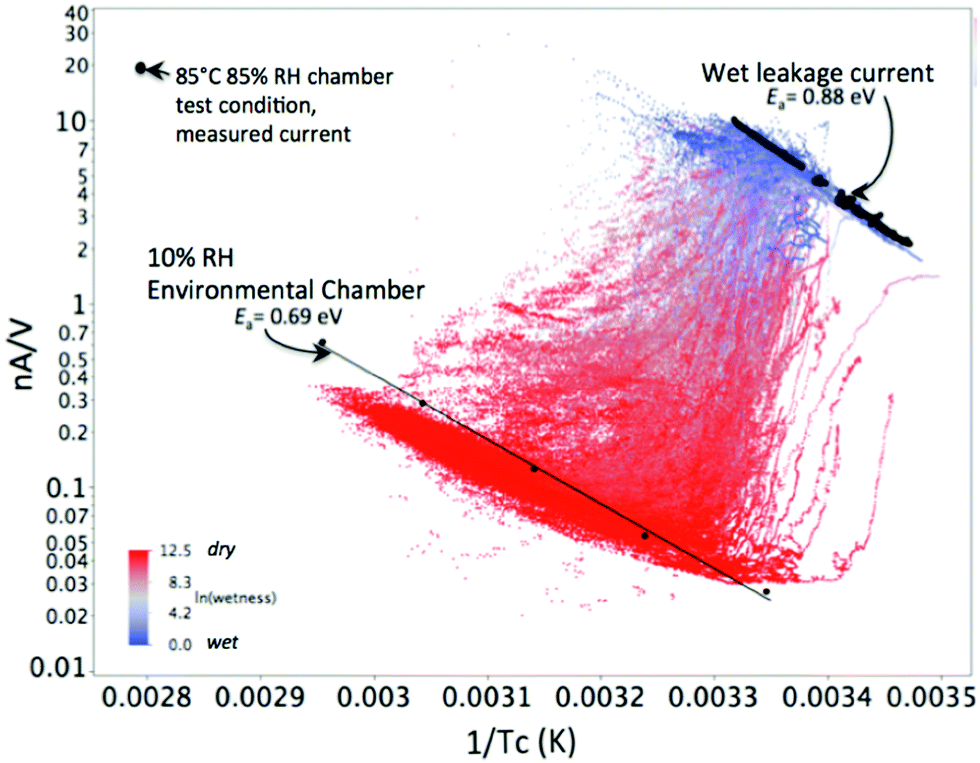 | ||
| Fig. 20 System voltage-normalized current over a period of about six months for a module held by edge clips (frameless) in Florida, USA (red-blue data, where blue is wet and red is dry according to the wetness sensor). Results in a dry chamber (10% RH, five lower points), wet leakage current tests (upper data), and for the 85 °C/85% RH chamber test conditions performed on a sister module are superimposed in black. Reprint from ref. 126. Copyright 2016, IEEE. | ||
Using a replica module of the module type shown in Fig. 20 current transferred as a function of temperature in a dry (10% RH) climate chamber, under the 85 °C/85% RH stress test condition, and again in a wet leakage current test apparatus applying −1000 V to the cell circuit are measured and superimposed on the outdoor data.126 Wet leakage current behavior matches well with the upper limit of current transferred outdoors, but there is some mismatch when the module is dry and hot. However, it is seen that the current transfer behavior of the two important extremes seen in the natural environment (wet and dry) can be quickly and easily characterized.126 When the current transfer from the module type in an environmental test chamber with test condition of 85 °C/85% RH is compared, the current transfer resembles that of periods the module is hot and wet in the natural environment, approximately 20 nA per volt of system voltage applied (nA V−1), though the current transfer paths may not necessarily be the same.
The determined relationships between current transfer and module conditions in Florida for regimes of (1) morning dew or rain, where a simple Arrhenius function when the module is wet can be used; (2), the morning, after the condensation has dried; and (3), the afternoon, were projected onto a module temperature and field meteorological data in Colorado, USA, to show the charge transferred for a year in Colorado in Fig. 21.126 Summing up the current transfer data for Florida (Fig. 20) and Colorado (Fig. 21), total charge transferred in Colorado are found to be lower, calculated to be overall 19% of that of Florida, primarily associated with minimal morning dew and lower humidity.
 | ||
| Fig. 21 Calculated current transfer from a module in Colorado, showing current transfer with Arrhenius relationship when the module is wet, and the result of the regression function derived from Florida data when humidity is uncondensed. Reprint from ref. 126.Copyright 2016, IEEE. | ||
5.6. Correlation between shunt resistance and PID-s
A direct result of PID-s in p-type c-Si PV modules is significant shunting in the solar cells. In the first approximation, the reciprocal of the shunt resistance is proportional to the power loss. Several publications have attempted to monitor the power loss due to PID-s by measuring the ohmic shunt resistance (Rsh) of PV modules and then simulating the module performance with the two-diode model assuming only a reduction in ohmic shunt resistance.36,62 Both Hacke et al. and Taubitz et al. reported that there is apparent discrepancy between the power loss measured by a solar simulator and simulated by the Rsh-based technique for full-size modules.36,62 To investigate the poor correlation, Hacke et al. fitted the dark current–voltage (I–V) curves with the two-diode model and concluded that J02 and n2 of the second diode term increased (recombination current or non-linear shunting) after PID-s.36 Taubitz et al. also drew the same conclusion, as modelling of the non-linear shunt yielded much better agreement between the measured and simulated results.62 More recently, this has been verified by the local I–V curve calculation through DLIT measurements.63,127 It was shown that the PID-s region exhibited a strongly increased J02 and an ideality factor n2 (larger than 2) due to increased recombination in the depletion region (Fig. 22).63 Therefore, assuming a reduction in ohmic shunt resistance alone is not sufficiently accurate to estimate module performance as PID-s progresses. The increase in J02 and n2 of the second diode term due to PID-s needs to be considered for better correlation. On the other hand, the mismatching effect between the solar cells that are degraded to different extents due to PID-s introduces additional errors to the Rsh-based technique when it is used for full-size modules. | ||
| Fig. 22 (a) EL image of a degraded solar cell; (b) DLIT image at −1 V; (c) J02 distribution calculated from DLIT measurements based on the method reported in ref. 128; (d) Ideality factor n2 distribution, scaled from 2 to 10. Reprint from ref. 63. Copyright 2014, IEEE. | ||
6. Preventive measures against PID in standard c-Si PV modules
Considering the catastrophic effects on PV modules, preventive measures have been developed to minimize PID effects on conventional p-type c-Si PV modules under outdoor conditions. In this section, the various PID-resistant or PID-free technologies for conventional p-type PV modules are summarized, which are categorized into three groups: a cell, a module and a system. Their advantages and disadvantages are also elaborated. At the cell level, the relevance of the properties of the SiNx AR coating on PID effects is discussed. PID-resistant cell technology can be achieved through modifications of the AR coating. It is also shown that additional pre-treatment steps prior to SiNx deposition can slow down PID effects. At the module level, PID can be minimized or avoided by judicious selection of the encapsulant and glass or superstate materials. Finally, at the system level, PID effects can be minimized with suitable system topologies. Some of these methods are also applicable to other types of module technologies (e.g. thin-film technologies) to inhibit PID effects, particularly at the module and system levels.6.1 Cell level
In addition, Nagel et al. compared the difference between two growth methods for the SiO2 film: ultraviolet (UV) oxidation and inline thermal oxidation.139 From their study, while both UV oxidized and thermally oxidized solar cells exhibited excellent PID stability, the thermally oxidized solar cells demonstrated a superior PID performance than those UV oxidized.139 Moreover, the thermally oxidized cells gained a 0.2% increase in efficiency, compared to the reference cells without oxidation prior to PID testing; but a 0.3% efficiency loss was observed in UV oxidized cells.139 The advantage of the UV oxidation process is that it can be retrofitted to existing cell production lines with minimal modifications in the system. They further fabricated modules with UV oxidized cells and stressed them under 85 °C, −2000 V conditions with Al foil on top of the cover glass.139 These modules suffered no power degradation for the first 6 days. However, they lost more than 10% of their initial power after 9 days.139 This could imply that the effect of the additional SiO2 delays PID-s rather than preventing it from occurring. Therefore, the long-term reliability of this technique has to be examined. It should also be noted that the SiO2 film in this section is intentionally grown, while the SiOx layer in Fig. 6 is the native oxide layer. The intentionally-grown layer is more likely to be thicker than the native oxide layer.
There is also another method reported in the literature to reduce PID-s sensitivity prior to SiNx deposition. Mehlich et al. applied a surface quality improvement technique, using energy-rich UV, to improve the reliability of solar cells under high-voltage stress.109,141 However, the fundamentals of the increased PID resistance were not discussed in their publications.
6.2. Module level
An alternative solution is to apply a coating on the glass to inhibit the ion migration and thus reduce the leakage current. Hacke and his coworkers tested PID sensitivity with commercially available glass coated with thin SiO2 film, which showed only modest PID resistance.15 Hara et al. deposited a thin TiO2 film on the cell side of the front soda-lime glass to suppress the drift of metal ions.144 The modules fabricated with these TiO2-coated glass sheets exhibited excellent protection against high-voltage stress (Fig. 23).144 A similar study was also conducted by Pop et al. using different coating materials.145 Their study also showed modestly improved PID resistance.145 However, the optical performance of these modules is reduced substantially, as the extra film reflects, scatters and absorbs the incident light. This leads to a reduced light intensity received by the active solar cells and hence a decreased module efficiency. There is also a third approach reported in the literature to resolve PID-s at the glass level in the literature. In this method, the PID effects are mitigated by disrupting the glass surface's conductivity under damp heat conditions106 with glass strips146 or chemical agents.147
 | ||
| Fig. 23 EL images of a standard module and the modules with the TiO2 coated cover glass before and after the PID test: (a) standard module, (b) module with a 50 nm-TiO2 film deposited on the cell side of the cover glass, and (c) module with a 100 nm-TiO2 deposited on the cell side of the cover glass. The standard module was seriously shunted after the PID test, while the module with 50 nm-TiO2 was less affected and the module with 100 nm-TiO2 appeared to be unaffected. Reprint from ref. 144. Copyright 2014, RSC Advances. | ||
In general, polyolefin, ionomer and silicone-based encapsulation materials possess a bulk resistivity that is 1 to 3 orders of magnitude higher than that of standard EVA materials at ambient temperature, see Table 1.42,149–151,154,158,159 It is also shown in Table 1 that they have a higher transmittance, compared to standard EVA. Therefore, these encapsulation materials can be used to substitute EVA to minimize PID effects at the module level without optical loss. This has already been verified in several reports,42,86,150,151,154,160 where modules fabricated with these materials exhibited high efficiency and negligible power degradation after PID testing in a harsh environment. Alternatively, instead of replacing EVA completely with other materials, Kapur et al. designed a bilayer structure of the ionomer (50/100/150 μm) and EVA (450 μm) to reduce the cost.155 For some types of ionomer, the 50 μm ionomer and 450 μm EVA configuration exhibited high PID sensitivity.155 However, when the thickness of the ionomer increased to 100 μm or 150 μm, this innovative design can significantly improve the PID resistance.149,155,157 In recent years, PID-resistant EVA materials were also developed with a higher bulk resistivity (in the order of 1015 Ω cm), and they have also shown improved PID-suppressing properties.42,149,154,155,161
| Encapsulant material | Volume resistivity (Ω cm) | Transmittance (%) | WVTR (g (m−2 day−1)) |
|---|---|---|---|
| EVA | 1.0 × 10¹⁴ | 91.0 | 34.00 |
| PVB | 4.8 × 10¹² | 91.0 | 40.05 |
| TPU | 2.7 × 10¹⁴ | 90.0 | |
| Silicone | 6.0 × 10¹⁵ | 98.9 | |
| Polyolefin | 2.0 × 10¹⁶ | 92.0 | 3.30 |
| Ionomer | 7.1 × 10¹⁶ | 93.4 | 0.19 |
The temperature effect on the bulk resistivity of encapsulation materials also has to be considered too. The operating temperature of solar panels in the fields may exceed 60 °C in hot climates,52 which leads to a reduced bulk resistivity of encapsulation materials (Arrhenius-type relationship).149,161 The bulk resistivity of standard EVA can drop to the range of 1011 to 1013 Ω cm under outdoor conditions, which is insufficient to prevent PID.42,149,151,161 However, polyolefin, ionomers and silicone-based encapsulation materials are less sensitive to the temperature. They still possess a bulk resistivity of above 1015 Ω cm under field-relevant conditions, which makes them more ideal for addressing PID at the module level.42,149,151
Furthermore, the moisture vapor transmission rate (MVTR) of encapsulation materials is a useful parameter for assessing the PID sensitivity. It is well known that moisture ingress will promote the progress of PID in PV modules.42,66,159 Encapsulation materials with a lower MVTR offer better protection against moisture penetration and are therefore favorable for reducing PID. This property will become more important when the modules are to be placed in humid environments. Reid et al. compared the PID-resistance of two polyolefin materials with the same bulk resistivity but different MVTR, and concluded that low MVTR can alleviate PID effects in the long term.154 However, a high MVTR does not necessarily mean that the material is PID sensitive. Berghold et al. revealed that a thermoplastic silicone elastomer material with high a MVTR value (38.5 g m−2 d−1) performed much better under high-voltage stress than the standard EVA (<10 g m−2 d−1).42 This was due to their different bulk resistivities.42 Therefore, it is not sufficient to assess the PID-suppressing property of encapsulation materials solely based on their MVTR. Instead, all three properties (bulk resistivity, temperature coefficient and WVTR) should be considered carefully when it comes to selecting proper encapsulation materials for PID-free PV modules. Moreover, production cost and other durability features such as adhesion, mechanical properties, UV-absorption need to be taken into careful consideration as well. These PID-resistant encapsulation materials have to be cost-competitive in order to gain market share.
The PID countermeasures at both the cell and module level can be explained consistently by a voltage divider model.134,135 It is based on the well-known assumption that the strength of the electric field in the SiNx layer is the driving force for the evolution of PID-s.134 A simplified model for the main leakage current path consists of a series connection of three ohmic resistors, one for each layer (glass, encapsulant foil, SiNx AR coating on the solar cell).134 In the first approximation, the leakage current is the same in all layers (path 1 in Fig. 2, see Section 2). According to Fig. 24, the voltage across the SiNx layer can be approximated by:134
 | (6) |
 | ||
| Fig. 24 Layer stack at the front of a c-Si solar module representing a voltage divider upon leakage currents. Each layer is modelled as a single resistor. | ||
6.3. System level
In a PV system, an inverter is an essential part of the balance of system (BOS), which converts the DC output into AC output. Based on the topologies, inverters can be broadly categorized into two groups: a transformer-based and a transformerless inverter.162,163 For the transformer-based inverter technology, either the negative or positive system pole has to be grounded, leading to either a positively-biased or negatively-biased solar cells relative to ground.12,13 As discussed in Sections 3.1.1 and 5.3, negatively-biased p-type c-Si PV modules are susceptible to PID-s, which are in general more detrimental to the module performance in the field. Therefore, a simple solution to PID-s for PV systems with a transformer-based inverter is to ground the negative system pole. This will ensure that all the modules will be positively biased, eliminating the PID-s in conventional p-type c-Si PV modules.However, there is a strong trend in the PV industry to use transformerless topologies.162,164–166 Not only are the transformerless inverters compact and light, more importantly this technology increases the conversion efficiency of PV systems by 1% to 2%.162 For a transformerless inverter, no galvanic isolation is present in the PV system and it also requires no grounding. This topology results in a floating potential, meaning that some cells are negatively biased and others are positively biased relative to ground.12,13 Therefore, the PID-s solution for the PV systems using transformer-based inverters is not applicable for those using transformerless inverters. A counter measure of PID-s problem for systems with transformerless inverters can be applying a reverse bias voltage (e.g. +1000 V) to the modules during night time.12,13,137 This can accelerate the recovery of the PV modules and regenerate the PV efficiency lost during the day time. This method is also applicable to systems with transformer-based inverters. However, the drawback is that it requires additional electronic components. Another innovative solution is the virtual DC bus concept for transformerless inverters.167 The topology allows the negative system pole to be virtually grounded and thereby shifting the solar cells' potential to the positive; hence the PV modules can be protected against PID-s.
There is also growing interest in the PV industry to use micro-inverters. These inverters are placed on every module such that the voltage of each module is optimized to the maximum power voltage,168 in the range of 30 V to 40 V for conventional c-Si PV modules. The driving force for PID in the field is then reduced, and modules that might show susceptibility at higher string voltages (600 V, 1000 V, 1500 V) could perform well with respect to PID over the long term at the much lower system voltage when controlled using a micro-inverter.59
7. PID recovery in standard c-Si PV modules
PID-s is detrimental to the performance of p-type c-Si PV modules. However, different from the TCO corrosion of thin-film modules, it has been found to be reversible.12,13 The underlying mechanism for PID-s recovery in conventional p-type c-Si PV modules was examined extensively by Lausch et al.72 In Fig. 25, EBIC images of a PID shunt before and after recovery are shown. The PID-shunted site has vanished after 2.5 hours of thermal recovery in a 250 °C environment. Out-diffusion of Na atoms from the stacking faults has been proposed to be responsible for PV efficiency regeneration. It is perceived that Na atoms slowly move out of the stacking faults into the oxide layer due to the concentration difference after the degradation process has stopped.72 The assumption is further supported by their investigation of the PID-shunted locations at the atomic level using high-angle annular dark field (HAADF) STEM.71,72 Before the recovery process, the crystal structure of the stacking fault could not be visualized clearly (the dark region around the stacking fault, Fig. 26a), as the silicon structure is strongly disturbed most likely by Na atoms within the Si matrix.71,72 However, a clean stacking fault was retained (Fig. 26b) after the recovery process and the disorder of the crystal structure could be easily visualized, indicating that Na atoms had diffused out of the stacking fault.71,72 Once the Na atoms diffuse out of the stacking fault, the electronic properties of the solar cells are restored.72 These findings again validate the stacking fault model for the PID-s in p-type c-Si PV modules. Moreover, it was previously discussed that the stacking fault may not exist in Si prior to PID stress,83 but after the recovery the extrinsic stacking fault did not vanish in one reported sample.63,71 This could imply that the recovered cells/modules may degrade at a faster rate during a second round of PID stress as stacking faults are already present in Si. The experimental data, however, show an opposite effect. After recovery in power from PID-s, following up with higher or longer PID-s stress levels results in less power loss than that associated with the first application of stress.32,43 Further study to explain these observations is required.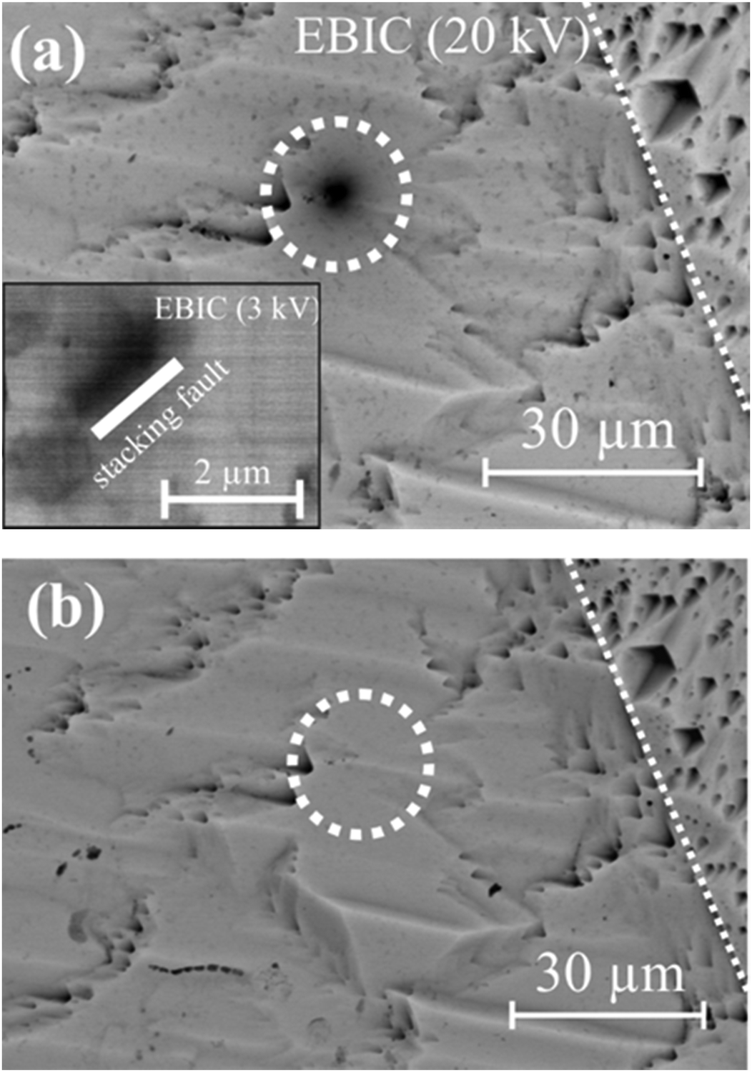 | ||
| Fig. 25 EBIC measurements (20 kV) at a PID shunt location before (a) and after (b) a thermal recovery process. The PID-s disappeared after recovery. The inset in (a) shows the PID-s defect before recovery at la low electron acceleration voltage (3 kV) and hence with an increased lateral resolution. The dotted line represents a grain boundary as guide to the eyes. Reprint from ref. 72. Copyright 2014, Elsevier. | ||
 | ||
| Fig. 26 HAADF STEM investigations of the Na-decorated stacking fault before (a) and after (b) thermal recovery. Before the recovery, the stacking fault is strongly disturbed, causing a dark region around the stacking fault. After recovery, the disorder of the stacking fault can be easily identified, which may be explained by the out-diffusion of Na during recovery. Reprint from ref. 72. Copyright 2014, Elsevier. | ||
Thermal recovery, reverse-biased voltage recovery and their combination have been identified to be able to recover the efficiency of p-type c-Si PV modules.12,13 These techniques are also applicable to other PV technologies (e.g. CIGS).91,137 Thermal recovery is temperature activated regeneration of the power lost due to PID-s. The rate of regeneration process increases with module temperature,62,116,120,122,169 but it is not observed that humidity accelerates the recovery.120 Taubitz et al. observed that the regeneration process is Arrhenius-like.62,169 This behavior agrees with the out-diffusion model, in which it is assumed that Na atoms diffuse out of the stacking faults due to the concentration difference (Fig. 27a).72 It is well known that diffusion is a temperature-controlled process;114 therefore, an increase in temperature will lead to a faster recovery rate. Even at room temperatures, PID-damaged modules can regain most of their initial power at STC after a long period of stabilization.137,143,170 This indicates that PID-affected modules in the fields can recover during the night-time when no bias voltage is applied. In addition, the regeneration process is also affected by the extent of the PID pre-damage.120 Hattendorf et al. stressed four full-size p-type c-Si PV modules to different extents under the same climatic conditions and with different bias voltages, prior to thermal recovery.120 Subsequently, these PID-affected modules were recovered under 70 °C and 50% RH conditions. It was found that the recovery process is dependent on the module's PID history;120 hence the amount of the previous PID damage plays a significant role.
 | ||
| Fig. 27 Schematic diagram of the proposed process for thermal recovery (a) and electrical recovery (b). The green dots represent the Na specie. Na diffuses out of the stacking faults, which leads to power regeneration. The movement of Na is marked by the white arrows. Reproduced from ref. 72. Copyright 2014, Elsevier. | ||
Another recovery method is to apply a reserve voltage (e.g. +1000 V) to the solar cells in the PID-damaged modules.12,13,137,143,170,171 This again can be explained by the out-diffusion model (Fig. 27b).72 When a reverse bias is applied, Na+ are driven away from the interface, creating a greater concentration gradient of Na between the Na-decorated stacking faults and the interface. As a result, the diffusion process will be accelerated. Even a nearly 100% percent power recovery at STC was observed,12,13 when p-type c-Si PV modules were subjected to a positive potential of 1000 V for less than 100 hours. Furthermore, this technique has been adopted in several industrial products (e.g. the SMA's PV offset box172 and the iLUMEN's PID box173) to prevent PID effects under the field conditions. These products apply a reverse voltage (e.g. +1000 V) to the module string during the night time to recover the PV power lost in the day, thereby preventing PID effects in the field. However, the method that applies a reverse bias at night when there is no sun to dry saturated modules also imparts stress leading to elevated leakage current in the opposite direction, which may over time lead to degradation of the module, such as by electrochemical corrosion.105
The recovery process may not be instantly initiated after the bias voltage has stopped. Taubitz et al. observed that the shunt resistance of a PID-affected mini-module continued to drop even after the voltage is stopped,62,169 and determined that there is a transition phase between the degradation and recovery, based on their shunt resistance measurements (Fig. 28).62,169 This may be explained by a concentration gradient-driven diffusion process of Na+ continuing into Si, which ends when the concentration gradient sufficiently dissipates. The duration of the transition phase was also found to be temperature dependent (Arrhenius-like).169 However, the transitional phase was not observed in another sample. It might be due to their different PID history, but the root cause was not investigated in the publications.169
 | ||
| Fig. 28 R sh measurements (normalized) of two one-cell modules during degradation and regeneration. One module exhibits the transition phase (marked by red) whereas the other module does not (marked by blue). The shunting phase (A), the transition phase (B) and the regeneration phase (C) are shown using different colours. The initial Rsh value (normalized) of both modules is more than 1 MΩ cm2, which is not shown in the figure. Reprint from ref. 62. Copyright 2013, WIP. | ||
Furthermore, incomplete recovery of PV efficiency at low irradiance levels and shunt resistance has also been reported, even after a long stabilization time and a near full recovery of power at STC.143,170 Oh et al. monitored the recovery process (room temperature and no reverse voltage) of a PID-affected sample for more than 200 days, but no complete recovery was obtained.143,170 It is suspected that residual Na remains in the stacking fault and causes the incomplete recovery.143,170 However, the assumption has yet to be verified with experimental evidence. Therefore, additional work is needed in the future to gain a better understanding of the recovery process.
8. Summary
In this paper, the most recent research progress in PID of PV modules is reviewed. Due to a high electrical potential difference, five leakage current pathways have been identified in PV modules. Their relative importance depends on the environmental conditions as well as the packaging materials. Significant progress has been made towards understanding the underlying principles causing the PV efficiency loss due to PID in different types of modules. Whether it is thin-film or c-Si based technologies, sodium ion (Na+) migration plays a crucial role in the evolution of PID. Electrochemical corrosion of the TCO layer, the surface polarization effect and PID-shunting (PID-s), respectively, are three of the most common PID mechanisms in thin-film modules, n-type c-Si modules and standard p-type c-Si modules, respectively. In particular, the Na-decorated stacking fault model provides an explanation for the PID effects often observed in p-type c-Si modules. Four types of test methods are available to evaluate the PID susceptibility at both the cell and module level. At a module level, chamber PID and Al PID tests are often used, while at a cell level, PID sensitivity can be examined by a corona discharge PID set-up or bias voltage application on a module-like layer stack.The majority of the PID studies performed so far dealt with standard p-type c-Si modules, as they dominate the present PV market. The progression of PID-s in standard c-Si modules depends on the applied voltage, humidity, and temperature. The leakage current shows an Arrhenius-type relationship with the temperature. Humidity and the applied voltage also affect the PID in multiple ways. Several kinetic models have been proposed to predict PID rates in p-type c-Si modules with meteorological data. Various methods have also been found to effectively prevent PID in p-type c-Si modules. At the cell level, the PID resistance can be improved by: (1) adjusting the Si/N ratio of the AR coating to a higher value to increase the electrical conductivity; (2) growing an interlayer (SiO2) between the Si and the SiNx AR coating; and (3) cleaning the cell surface with energy-rich UV prior to SiNx deposition. At the module level, PID can be prevented by using encapsulation materials or/and glass sheets with high bulk resistivity. At the system level, PID-s can be mitigated by ensuring that the active circuit of PV modules is not negatively biased relative to ground or applying a reverse voltage at night. Alternatively, it can be effectively prevented with application of micro-inverters. Moreover, PID-s in p-type c-Si PV modules were found to be reversible; thermal recovery, reverse-biased voltage recovery and their combination have been shown to be able to regenerate the PV efficiency loss. It has to be noted that most of the findings from p-type c-Si type modules are also applicable to other types of PV technologies (e.g. thin-film technology). For example, PID in thin-film modules can also be prevented by using an ionomer encapsulant.
Overall, an improved understanding of PID in PV modules has been obtained through continuous research in recent years. More PID-related research is anticipated to provide insights into the open questions that have yet to be fully understood. Some of the open questions are as follows: (1) there is relatively little understanding of the electronic structure of sodium (Na) contaminated stacking faults that have been attributed to shunting of the n+−p junction in conventional front-junction c-Si cells in several reports; (2) the partial recovery of power frequently observed for PID of the shunting type (PID-s) is yet not fully understood mechanistically; (3) while there are several published correlations between the chamber tests and the field results, more work is needed to correlate the test results with PID durability in specific climates so that appropriate PID-resistant modules can be designed; and (4) appropriate PID-resistant designs and materials whose performance, durability and cost requirements are still being explored. More importantly, the PV industry is facing a great challenge to prevent PID of PV modules, as many proposed solutions either compromise the efficiency or increase the cost. There is still a long way to go on the path towards developing completely PID-free PV technologies at low cost.
Acknowledgements
The work at the Solar Energy Research Institute of Singapore (SERIS) was sponsored by the National University of Singapore (NUS) and the National Research Foundation of Singapore through the Singapore Economic Development Board. The work at the National Renewable Energy Laboratory (Peter Hacke and Steven P. Harvey) was supported by the U.S. Department of Energy under Contract No. DE-AC36-08GO28308. Funding was provided by the SuNLaMP program of the Office of Energy Efficiency & Renewable Energy.References
- Solar Power Europe, Global market outlook for solar power 2016–2020, 2016.
- IEA, Snapshot of Global PV 2015, OECD/IEA, Paris, 2016 Search PubMed.
- IEA, Technology roadmap: solar photovoltaic energy, OECD/IEA, Paris, 2014 Search PubMed.
- D. C. Jordan and S. R. Kurtz, Prog. Photovoltaics, 2013, 21, 12–29 Search PubMed.
- D. Polverini, M. Field, E. Dunlop and W. Zaaiman, Prog. Photovoltaics, 2013, 21, 1004–1015 Search PubMed.
- A. Pozza and T. Sample, Prog. Photovoltaics, 2015, 24, 368–378 Search PubMed.
- T. Ishii, T. Takashima and K. Otani, Prog. Photovoltaics, 2011, 19, 170–179 CAS.
- V. Sharma and S. Chandel, Renewable Sustainable Energy Rev., 2013, 27, 753–767 CrossRef.
- A. Ndiaye, A. Charki, A. Kobi, C. M. Kébé, P. A. Ndiaye and V. Sambou, Sol. Energy, 2013, 96, 140–151 CrossRef.
- M. Munoz, M. Alonso-Garcia, N. Vela and F. Chenlo, Sol. Energy, 2011, 85, 2264–2274 CrossRef CAS.
- C. Dechthummarong, B. Wiengmoon, D. Chenvidhya, C. Jivacate and K. Kirtikara, Sol. Energy Mater. Sol. Cells, 2010, 94, 1437–1440 CrossRef CAS.
- J. Berghold, O. Frank, H. Hoehne, S. Pingel, B. Richardson and M. Winkler, Proceedings of the 25th European Photovoltaic Solar Energy Conference and Exhibition, Valencia, Spain, 2010, pp. 3753–3759 Search PubMed.
- S. Pingel, O. Frank, M. Winkler, S. Daryan, T. Geipel, H. Hoehne and J. Berghold, Proceedings of the 35th IEEE Photovoltaic Specialists Conference, Honolulu, HI, USA, 2010, pp. 2817–2822 Search PubMed.
- P. Hacke, K. Terwilliger, S. Glick, D. Trudell, N. Bosco, S. Johnston and S. Kurtz, Proceedings of the 35th IEEE Photovoltaic Specialists Conference, Honolulu, HI, USA, 2010, pp. 000244–000250 Search PubMed.
- P. Hacke, M. Kempe, K. Terwilliger, S. Glick, N. Call, S. Johnston, S. Kurtz, I. Bennett and M. Kloos, Proceedings of the 25th European Photovoltaic Solar Energy Conference and Exhibition, Valencia, Spain, 2010, pp. 3760–3765 Search PubMed.
- J. Berghold, S. Koch, S. Pingel, S. Janke, A. Ukar, P. Grunow and T. Shioda, Proceedings of SPIE, San Diego, CA, USA, 2015, vol. 9563, p. 95630A Search PubMed.
- E. Schneller, N. S. Shiradkar and N. G. Dhere, Proceedings of the 40th IEEE Photovoltaic Specialists Conference, Denver, CO, USA, 2014, pp. 3216–3219 Search PubMed.
- R. Malachi, S. Schönberger, J. Mayer and M. Kasemann, Proceedings of the 29th European Photovoltaic Solar Energy Conference and Exhibition, Amsterdam, The Netherlands, 2014, pp. 2323–2326 Search PubMed.
- G. Mon, L. Wen, R. Ross and D. Adent, Proceedings of the 18th IEEE Photovoltaic Specialists Conference, Las Vegas, NV, USA, 1985, pp. 1179–1185 Search PubMed.
- G. Mon and R. Ross, Proceedings of the 18th IEEE Photovoltaic Specialists Conference, Las Vegas, NV, USA, 1985, pp. 1142–1149 Search PubMed.
- D. Carlson, R. Romero, F. Willing, D. Meakin, L. Gonzalez, R. Murphy, H. Moutinho and M. Al Jassim, Prog. Photovoltaics, 2003, 11, 377–386 CAS.
- C. Osterwald, T. McMahon and J. Del Cueto, Sol. Energy Mater. Sol. Cells, 2003, 79, 21–33 CrossRef CAS.
- J. Del Cueto and T. McMahon, Prog. Photovoltaics, 2002, 10, 15–28 CAS.
- N. G. Dhere, S. M. Bet and H. P. Patil, Proceedings of 3rd World Conference on Photovoltaic Energy Conversion, Osaka, Japan, 2003, vol. 2, pp. 1923–1926 Search PubMed.
- N. G. Dhere, M. B. Pandit, A. H. Jahagirdar, V. S. Gade, A. A. Kadam, S. S. Kulkarni, N. S. Mehta, S. M. Bet and H. P. Patil, Proceedings of NCPV program Review Meeting, Lakewood, CO, USA, 2001, pp. 313–314 Search PubMed.
- T. McMahon and G. Jorgensen, Proceedings of 2001 NCPV Program Review Meeting, Lakewood, CO, USA, 2001, pp. 137–138 Search PubMed.
- R. Swanson, M. Cudzinovic, D. DeCeuster, V. Desai, J. Jürgens, N. Kaminar, W. Mulligan, L. Barbarosa, D. Rose and D. Smith, Proceedings of 15th International Photovoltaic Science and Engineering Conference, Shanghai, China, 2005, pp. 410–411 Search PubMed.
- I. Rutschmann, Photon, 2008, 1, 122–123 Search PubMed.
- I. Rutschmann, Photon, 2008, 8, 124–125 Search PubMed.
- P. Hacke, R. Smith, K. Terwilliger, S. Glick, D. Jordan, S. Johnston, M. Kempe and S. Kurtz, Proceedings of 2013 IEEE International Reliability Physics Symposium (IRPS), Anaheim, CA, USA, 2013, pp. 4B.1.1–4B.1.5 Search PubMed.
- P. Hacke, R. Smith, K. Terwilliger, G. Perrin, B. Sekulic and S. Kurtz, Prog. Photovoltaics, 2014, 22, 775–783 Search PubMed.
- P. Hacke, K. Terwilliger, R. Smith, S. Glick, J. Pankow, M. Kempe, S. K. I. Bennett and M. Kloos, Proceedings of the 37th IEEE Photovoltaic Specialists Conference, Seattle, WA, USA, 2011, pp. 000814–000820 Search PubMed.
- V. Naumann, C. Hagendorf, S. Grosser, M. Werner and J. Bagdahn, Energy Procedia, 2012, 27, 1–6 CrossRef CAS.
- V. Naumann, D. Lausch, S. Großer, M. Werner, S. Swatek, C. Hagendorf and J. Bagdahn, Energy Procedia, 2013, 33, 76–83 CrossRef CAS.
- V. Naumann, D. Lausch, A. Graff, M. Werner, S. Swatek, J. Bauer, A. Hähnel, O. Breitenstein, S. Großer and J. Bagdahn, Phys. Status Solidi RRL, 2013, 7, 315–318 CrossRef CAS.
- P. Hacke, R. Smith, K. Terwilliger, S. Glick, D. Jordan, S. Johnston, M. Kempe and S. Kurtz, Proceedings of the 38th IEEE Photovoltaic Specialists Conference, Austin, TX, USA, 2012, pp. 1–8 Search PubMed.
- M. Gossla, T. Hälker, S. Krull, F. Rakusa, F. Roth and I. Sinicco, Proc. SPIE, San Diego, CA, USA, 2010, vol. 7773, p.77730O Search PubMed.
- S. Voswinckel, P. Manz, C. Schmidt, V. Wesselak, E. Fokuhl and B. Trautmann, Proceedings of the 28th European Photovoltaic Solar Energy Conference and Exhibition, Paris, France, 2013, pp. 2478–2483 Search PubMed.
- T. M. Walsh, Z. Xiong, Y. S. Khoo, A. A. Tay and A. G. Aberle, Energy Procedia, 2012, 15, 388–395 CrossRef.
- Z. Xiong, T. M. Walsh and A. G. Aberle, Energy Procedia, 2011, 8, 384–389 CrossRef CAS.
- V. Fjällström, P. Salomé, A. Hultqvist, M. Edoff, T. Jarmar, B. Aitken, K. Zhang, K. Fuller and C. K. Williams, IEEE Journal of Photovoltaics, 2013, 3, 1090–1094 CrossRef.
- J. Berghold, S. Koch, B. Frohmann, P. Hacke and P. Grunow, Proceedings of the 40th IEEE Photovoltaic Specialists Conference, Denver, CO, USA, 2014, pp. 1987–1992 Search PubMed.
- M. Schütze, M. Junghänel, M. Koentopp, S. Cwikla, S. Friedrich, J. Müller and P. Wawer, Proceedings of the 37th IEEE Photovoltaic Specialists Conference, Seattle, WA, USA, 2011, pp. 000821–000826 Search PubMed.
- N. G. Dhere, N. S. Shiradkar and E. Schneller, IEEE Journal of Photovoltaics, 2014, 4, 654–658 CrossRef.
- M. B. Koentopp, M. Krober and C. Taubitz, IEEE Journal of Photovoltaics, 2016, 6, 252–257 CrossRef.
- P. Hacke, K. Terwilliger, S. Glick, G. Tamizhmani, S. Tatapudi, C. Stark, S. Koch, T. Weber, J. Berghold and S. Hoffmann, IEEE Journal of Photovoltaics, 2015, 5, 94–101 CrossRef.
- P. Hacke, P. Burton, A. Hendrickson, S. Spataru, S. Glick and K. Terwilliger, Proceedings of the 42nd IEEE Photovoltaic Specialists Conference, New Orleans, LA, USA, 2015, pp. 1–4 Search PubMed.
- N. G. Dhere, N. S. Shiradkar and E. Schneller, Appl. Phys. Lett., 2014, 104, 112103 CrossRef.
- M. Schütze, M. Junghänel, O. Friedrichs, R. Wichtendahl, M. Scherff, J. Müller and P. Wawer, Proceedings of the 26th European Photovoltaic Solar Energy Conference and Exhibition, Hamburg, Germany, 2011, pp. 3097–3102 Search PubMed.
- N. Shiradkar, E. Schneller and N. G. Dhere, Proc. SPIE, San Diego, CA, USA, 2013, vol. 8825, p. 88250G Search PubMed.
- S. Hoffmann and M. Koehl, Prog. Photovoltaics, 2014, 22, 173–179 CAS.
- S. Hoffmann and M. Köhl, Proceedings of the 28th European Photovoltaic Solar Energy Conference and Exhibition, Paris, France, 2013, pp. 3336–3339 Search PubMed.
- A. McEvoy, T. Markvart, L. Castañer, T. Markvart and L. Castaner, Practical handbook of photovoltaics: fundamentals and applications, Elsevier, 2003 Search PubMed.
- T. McMahon, Prog. Photovoltaics, 2004, 12, 235–248 CAS.
- N. G. Dhere, V. V. Hadagali and S. M. Bet, Proceedings of the 19th European Photovoltaic Solar Energy Conference and Exhibition, Paris, France, 2004 Search PubMed.
- S. Voswinckel, V. Wesselak, E. Fokuhl, C. Schmidt and K. Watzlawik, Proceedings of the 31st European Photovoltaic Solar Energy Conference and Exhibition, Hamburg, Germany, 2015, pp. 2508–2512 Search PubMed.
- P. Manz, V. Wesselak, S. Voswinckel, B. Trautmann, E. Fokuhl and C. Schmidt, Proceedings of the 29th European Photovoltaic Solar Energy Conference and Exhibition, Amsterdam, The Netherlands, 2014, pp. 3194–3199 Search PubMed.
- P. Lechner, S. Hummel, D. Geyer and H. Mohring, Proceedings of the 28th European Photovoltaic Solar Energy Conference and Exhibition, Paris, France, 2013, pp. 2810–2815 Search PubMed.
- H. Nagel, A. Metz and K. Wangemann, Proceedings of 26th European Photovoltaic Solar Energy Conference and Exhibition, Hamburg, Germany, 2011, pp. 3107–3112 Search PubMed.
- N. G. Dhere, S. A. Pethe and A. Kaul, Proc. SPIE, San Diego, CA, USA, 2011, vol. 8112, p. 81120O Search PubMed.
- G. Mathiak, S. Kammer, M. Schweiger and W. Herrmann, Proceedings of the 28th European Photovoltaic Solar Energy Conference and Exhibition, Paris, France, 2013, pp. 3332–3335 Search PubMed.
- C. Taubitz, M. Schütze and M. B. Koentopp, Proceedings of the 27th European Photovoltaic Solar Energy Conference and Exhibition, Frankfurt, Germany, 2012, pp. 3172–3176 Search PubMed.
- D. Lausch, V. Naumann, O. Breitenstein, J. Bauer, A. Graff, J. Bagdahn and C. Hagendorf, IEEE Journal of Photovoltaics, 2014, 4, 834–840 CrossRef.
- J. Bauer, V. Naumann, S. Großer, C. Hagendorf, M. Schütze and O. Breitenstein, Phys. Status Solidi RRL, 2012, 6, 331–333 CrossRef CAS.
- V. Naumann, D. Lausch, A. Hähnel, J. Bauer, O. Breitenstein, A. Graff, M. Werner, S. Swatek, S. Großer and J. Bagdahn, Sol. Energy Mater. Sol. Cells, 2014, 120, 383–389 CrossRef CAS.
- S. Koch, C. Seidel, P. Grunow, S. Krauter and M. Schoppa, Proceedings of the 26th European Photovoltaic Solar Energy Conference and Exhibition, Hamburg, Germany, 2011, pp. 1726–1731 Search PubMed.
- U. K. Krieger and W. A. Lanford, J. Non-Cryst. Solids, 1988, 102, 50–61 CrossRef CAS.
- V. Naumann, D. Lausch and C. Hagendorf, Energy Procedia, 2015, 77, 397–401 CrossRef CAS.
- A. Raykov, H. Hahn, K. H. Stegemann, M. Kutzer, O. Storbeck, H. Neuhaus and W. Bergholz, Proceedings of the 28th European Photovoltaic Solar Energy Conference and Exhibition, Paris, France, 2013, pp. 2998–3002 Search PubMed.
- P. Saint-Cast, H. Nagel, D. Wagenmann, J. Schön, P. Schmitt, C. Reichel, S. W. Glunz, M. Hofmann, J. Rentsch and R. Preu, Proceedings of the 28th European Photovoltaic Solar Energy Conference and Exhibition, Paris, France, 2013, pp. 789–792 Search PubMed.
- V. Naumann, D. Lausch, A. Hähnel, O. Breitenstein and C. Hagendorf, Phys. Status Solidi C, 2015, 12, 1103–1107 CrossRef CAS.
- D. Lausch, V. Naumann, A. Graff, A. Hähnel, O. Breitenstein, C. Hagendorf and J. Bagdahn, Energy Procedia, 2014, 55, 486–493 CrossRef CAS.
- B. Ziebarth, M. Mrovec, C. Elsässer and P. Gumbsch, J. Appl. Phys., 2014, 116, 093510 CrossRef.
- S. Steingrube, O. Breitenstein, K. Ramspeck, S. Glunz, A. Schenk and P. P. Altermatt, J. Appl. Phys., 2011, 110, 014515 CrossRef.
- S. P. Harvey, J. Aguiar, P. Hacke, H. Guthrey, S. Johnston and M. Al-Jassim, IEEE Journal of Photovoltaics, 2016, 6, 1440–1445 CrossRef.
- A. Armigliato, M. Servidori, S. Solmi and I. Vecchi, J. Appl. Phys., 1977, 48, 1806–1812 CrossRef CAS.
- W. Tseng, S. Lau and J. Mayer, Phys. Lett. A, 1978, 68, 93–94 CrossRef.
- V. Ravi, Philos. Mag., 1974, 30, 1081–1090 CrossRef.
- S. Hu, J. Appl. Phys., 1974, 45, 1567–1573 CrossRef CAS.
- A. M. R. Lin, R. W. Dutton, D. A. Antoniadis and W. A. Tiller, J. Electrochem. Soc., 1981, 128, 1121–1130 CrossRef CAS.
- J. Hornstra, J. Phys. Chem. Solids, 1958, 5, 129–141 CrossRef CAS.
- O. Krivanek and D. Maher, Appl. Phys. Lett., 1978, 32, 451–453 CrossRef CAS.
- V. Naumann, C. Brzuska, M. Werner, S. Großer and C. Hagendorf, Energy Procedia, 2016, 92, 569–575 CrossRef CAS.
- A. Halm, A. Schneider, V. D. Mihailetchi, L. J. Koduvelikulathu, L. M. Popescu, G. Galbiati, H. Chu and R. Kopecek, Energy Procedia, 2015, 77, 356–363 CrossRef CAS.
- K. Hara, S. Jonai and A. Masuda, Sol. Energy Mater. Sol. Cells, 2015, 140, 361–365 CrossRef CAS.
- S. Yamaguchi, A. Masuda and K. Ohdaira, Sol. Energy Mater. Sol. Cells, 2016, 151, 113–119 CrossRef CAS.
- V. Naumann, T. Geppert, S. Großer, D. Wichmann, H.-J. Krokoszinski, M. Werner and C. Hagendorf, Energy Procedia, 2014, 55, 498–503 CrossRef CAS.
- S. Yamaguchi, S. Jonai, K. Hara, H. Komaki, Y. Shimizu-Kamikawa, H. Shibata, S. Niki, Y. Kawakami and A. Masuda, Jpn. J. Appl. Phys., 2015, 54, 08KC13 CrossRef.
- S. Voswinckel, P. Manz, C. Schmidt and V. Wesselak, Energy Procedia, 2014, 57, 56–64 CrossRef CAS.
- K. Jansen and A. Delahoy, Thin Solid Films, 2003, 423, 153–160 CrossRef CAS.
- V. Fjällström, P. Szaniawski, B. Vermang, P. M. Salome, F. Rostvall, U. Zimmermann and M. Edoff, IEEE Journal of Photovoltaics, 2015, 5, 664–669 CrossRef.
- P. Hacke, S. Spataru, S. Johnston, K. Terwilliger, K. VanSant, M. Kempe, J. Wohlgemuth, S. Kurtz, A. Olsson and M. Propst, IEEE Jounal of Photovoltaics, 2016, 6, 1635–1640 CrossRef.
- N. G. Dhere, V. V. Hadagali and K. Jansen, Proceedings of the 31st IEEE Photovoltaic Specialists Conference, Orlando, FL, USA, 2005, pp. 507–510 Search PubMed.
- C. Osterwald, T. McMahon, J. del Cueto, J. Adelstein and J. Pruett, National Center Photovoltaics Solar Program Review Meeting, Denver, CO, USA, 2003 Search PubMed.
- K. Sato, Y. Matsui, K. Adachi, Y. Gotoh, Y. Hayashi and H. Nishimura, Conference Record of the 23rd IEEE Photovoltaic Specialists Conference, Louisville, KY, USA, 1993, pp. 855–859 Search PubMed.
- IEC 61215, Second edition, 2005.
- IEC 61646, 2008.
- P. Hacke, K. Terwilliger, S. Koch, T. Weber, J. Berghold, S. Hoffmann, M. Koehl, S. Dietrich, M. Ebert and G. Mathiak, Results of IEC 62804 draft round robin testing, 2013 Search PubMed, http://www.nrel.gov/docs/fy13osti/60493.pdf, accessed 11/03, 2016.
- IEC TS 62804-1, Edition 1.0, 2015.
- IEC NP 62804-2 TS, 2015.
- F. A. Lindholm, J. G. Fossum and E. L. Burgess, IEEE Trans. Electron Devices, 1979, 26, 165–171 CrossRef.
- S. Spataru, P. Hacke, D. Sera, C. Packard, T. Kerekes and R. Teodorescu, Prog. Photovoltaics, 2015, 23, 1536–1549 Search PubMed.
- J. Berghold, P. Grunow, P. Hacke, W. Herrmann, S. Hoffmann, S. Janke, B. Jaeckel, S. Koch, M. Köhl and G. Mathiak, Proceedings of the 28th European Photovoltaic Solar Energy Conference and Exhibition, Paris, France, 2013, pp. 3003–3011 Search PubMed.
- K. Morita and K. Ohnaka, Ind. Eng. Chem. Res., 2000, 39, 4684–4688 CrossRef CAS.
- P. Hacke, K. Terwilliger, S. Glick, R. Smith, G. Perrin, S. Kurtz, N. Bosco and J. Wohlgemuth, Proceedings of 40th IEEE Photovoltaic Specialist Conference, Denver, CO, USA, 2014, pp. 0930–0936 Search PubMed.
- F. Ebneali, S. Tatapudi and G. TamizhMani, Proceedings of the 39th IEEE Photovoltaic Specialists Conference, Tampa, FL, USA, 2013, pp. 1548–1553 Search PubMed.
- H.-C. Liu, C.-T. Huang, W.-K. Lee and M.-H. Lin, Energy Power Eng., 2013, 5, 455 CrossRef.
- S. Pingel, S. Janke, J. Seydewitz, R. Alam, S. Koch, J. Kupke and J. Berghold, Proceedings of the 29th European Photovoltaic Solar Energy Conference and Exhibition, Amsterdam, The Netherlands, 2014, pp. 2335–2341 Search PubMed.
- H. Mehlich, D. Decker, U. Scheit, M. Uhlig, S. Frigge, M. Runge, B. Heinze, H.-P. Sperlich, J. Mai, H. Schlemm, E. Vetter, J. Höhne, S. Reichel and W. Stein, Proceedings of the 27th European Photovoltaic Solar Energy Conference and Exhibition, Frankfurt, Germany, 2012, pp. 3411–3413 Search PubMed.
- V. Naumann, D. Lausch, K. Ilse, O. Breitenstein, J. Bauer, S. Grosser, J. Bagdahn and H. C. Golden, Proceedings of NREL PV Module Reliability Workshop, Denver, CO, USA, 2014 Search PubMed.
- J. Bagdahn, Proceedings of the 43rd IEEE Photovoltaic Specialists Conference (in press), Portland, OR, USA, 2016 Search PubMed.
- M. Koentopp, Hanwha Q-cells, personal communication.
- H. Nagel, Patent, WO 2012168249 A3, 2012 Search PubMed.
- H. Mehrer, Diffusion in solids: fundamentals, methods, materials, diffusion-controlled processes, Springer Science & Business Media, 2007 Search PubMed.
- J. Del Cueto and S. Rummel, Proc. SPIE, San Diego, CA, USA, 2010, vol. 7773, p. 77730J Search PubMed.
- A. Raykov, H. Nagel, D. Amankwah and W. Bergholz, Proceedings of the 27th European Photovoltaic Solar Energy Conference and Exhibition, Frankfurt, Germany, 2012, pp. 3399–3404 Search PubMed.
- Z. Boksay, M. Varga and A. Wikby, J. Non-Cryst. Solids, 1975, 17, 349–358 CrossRef CAS.
- M. D. Kempe, Sol. Energy Mater. Sol. Cells, 2006, 90, 2720–2738 CrossRef CAS.
- J. Hattendorf, R. Loew, W. Gnehr, L. Wulff, M. Koekten, D. Kosnisharov, A. Blauaermel and J. Esquivel, Proceedings of the 27th European Photovoltaic Solar Energy Conference and Exhibition, Frankfurt, Germany, 2012, pp. 3405–3410 Search PubMed.
- J. Hattendorf, W. Gnehr, R. Löw, R. Roth, D. Kosnisharov and M. Zentgraf, Proceedings of the 28th European Photovoltaic Solar Energy Conference and Exhibition, Paris, France, 2013, pp. 3303–3308 Search PubMed.
- P. Hacke, S. Spataru, K. Terwilliger, G. Perrin, S. Glick, S. Kurtz and J. Wohlgemuth, IEEE Journal of Photovoltaics, 2015, 5, 1549–1553 CrossRef.
- C. Taubitz, M. Schütze, M. Kröber and M. B. Koentopp, Proceedings of the 29th European Photovoltaic Solar Energy Conference and Exhibition, Amsterdam, The Netherlands, 2014, pp. 2490–2494 Search PubMed.
- S. Koch, J. Berghold, B. Abdullah, C. Hinz and P. Grunow, Proceedings of the 29th European Photovoltaic Solar Energy Conference and Exhibition, Amsterdam, The Netherlands, 2014, pp. 3327–3333 Search PubMed.
- C. Taubitz, M. Kröber, D. Buß and M. B. Köntopp, Proceedings of the 31st European Photovoltaic Solar Energy Conference and Exhibition, Hamburg, Germany, 2015, pp. 1807–1812 Search PubMed.
- T. Weber, J. Berghold, F. Heilmann, M. Roericht, S. Krauter and P. Grunow, Proceedings of the 28th European Photovoltaic Solar Energy Conference and Exhibition, Paris, France, 2013, pp. 3324–3331 Search PubMed.
- P. Hacke, R. Smith, S. Kurtz, D. Jordan and J. Wohlgemuth, Proceedings of the 43rd IEEE Photovoltaic Specialists Conference (in press), Portland, OR, USA, 2016 Search PubMed.
- O. Breitenstein, Sol. Energy Mater. Sol. Cells, 2011, 95, 2933–2936 CrossRef CAS.
- S. Koch, D. Nieschalk, J. Berghold, S. Wendlandt, S. Krauter and P. Grunow, Proceedings of the 27th European Photovoltaic Solar Energy Conference and Exhibition, Frankfurt, Germany, 2012, pp. 1985–1990 Search PubMed.
- X. Gou, X. Li, S. Zhou, S. Wang, W. Fan and Q. Huang, Int. J. Photoenergy, 2015, 2015, 863248 CrossRef.
- K. Mishina, A. Ogishi and K. Ueno, Proceedings of the 28th European Photovoltaic Solar Energy Conference and Exhibition, Paris, France, 2013, pp. 1139–1143 Search PubMed.
- T.-M. Kuan, C.-C. Huang, L.-G. Wu, Y.-C. Chan and C.-Y. Yu, Proceedings of the 39th IEEE Photovoltaic Specialists Conference, Tampa, FL, USA, 2013, pp. 2224–2226 Search PubMed.
- S. C. Pop, R. Schulze, X. Wang, H. Wang, J. Nee, D. Inns, A. Meisel, J. Kapur and H. Antoniadis, Proceedings of the 31st European Photovoltaic Solar Energy Conference and Exhibition, Hamburg, Germany, 2015, pp. 15–19 Search PubMed.
- M. Wilson, A. Savthouck, J. D'Amico, J. Lagowski, S. Schmitt, A. Schneider and S. Olibet, Proceedings of the 39th IEEE Photovoltaic Specialists Conference, Tampa, FL, USA, 2013, pp. 0218–0222 Search PubMed.
- V. Naumann, K. IIse and C. Hagendorf, Proceedings of the 28th European Photovoltaic Solar Energy Conference and Exhibition, Paris, France, 2013, pp. 2994–2997 Search PubMed.
- R. M. Swanson, D. De Ceuster, V. Desai, D. H. Rose, D. D. Smith and N. Kaminar, Patent, US7554031 B2, 2009 Search PubMed.
- W. Soppe, H. Rieffe and A. Weeber, Prog. Photovoltaics, 2005, 13, 551–569 CAS.
- S. Pingel, S. Janke and O. Frank, Proceedings of the 27th European Photovoltaic Solar Energy Conference and Exhibition, Frankfurt, Germany, 2012, pp. 3379–3383 Search PubMed.
- W. Han, W. Shan, X. Niu, Q. Jiang, Y. Li, C. Lu, Z. Qiu and J. Li, Proceedings of the 28th European Photovoltaic Solar Energy Conference and Exhibition, Paris, France, 2013, pp. 3309–3312 Search PubMed.
- H. Nagel, P. Saint-Cast, M. Glatthaar and S. Glunz, Proceedings of the 29th European Photovoltaic Solar Energy Conference and Exhibition, Amsterdam, The Netherlands, 2014, pp. 2351–2355 Search PubMed.
- J. D. Moschner, H. Nagel, A. Lachowicz and M. Fiedler, Patent, US20150064835 A1, 2015 Search PubMed.
- http://www.meyerburger.com/en/products-systems/competences/coating/photovoltaics/industrial-coating-systems/sqi/, accessed 15/07, 2016.
- M. Kambe, K. Hara, K. Mitarai, S. Takeda, M. Fukawa, N. Ishimaru and M. Kondo, Proceedings of 42nd IEEE Photovoltaic Specialist Conference, Tampa, FL, USA, 2013, pp. 3500–3503 Search PubMed.
- J. Oh, S. Bowden and G. TamizhMani, IEEE Journal of Photovoltaics, 2015, 5, 1540–1548 CrossRef.
- K. Hara, H. Ichinose, T. N. Murakami and A. Masuda, RSC Adv., 2014, 4, 44291–44295 RSC.
- S. C. Pop, R. Schulze, B. Brophy, S. Maghsoodi, Y. S. Yang, Z. R. Abrams and P. Gonsalves, Proceedings of 42nd IEEE Photovoltaic Specialist Conference, New Orleans, LA, USA, 2015, pp. 1–6 Search PubMed.
- J. Oh, G. TamizhMani, S. Bowden and S. Garner, Proceedings of 42nd IEEE Photovoltaic Specialist Conference, New Orleans, LA, USA, 2015, pp. 1–4 Search PubMed.
- T. Yoshida and T. Hirano, Proceedings of the 31st European Photovoltaic Solar Energy Conference and Exhibition, Hamburg, Germany, 2015, pp. 146–148 Search PubMed.
- A. Luque and S. Hegedus, Handbook of photovoltaic science and engineering, John Wiley & Sons, 2011 Search PubMed.
- J. Kapur, K. M. Stika, C. S. Westphal, J. L. Norwood and B. Hamzavytehrany, IEEE Journal of Photovoltaics, 2015, 5, 219–223 CrossRef.
- M. López-Escalante, L. J. Caballero, F. Martín, M. Gabás, A. Cuevas and J. Ramos-Barrado, Sol. Energy Mater. Sol. Cells, 2016, 144, 691–699 CrossRef.
- K. Nanjundiah, J. Naumovitz, M. White and T. Burns, Proceedings of the 27th European Photovoltaic Solar Energy Conference and Exhibition, Frankfurt, Germany, 2012, pp. 3384–3387 Search PubMed.
- S.-H. Schulze, A. Apel, R. Meitzner, M. Schak, C. Ehrich and J. Schneider, Proceedings of the 28th European Photovoltaic Solar Energy Conference and Exhibition, Paris, France, 2013, pp. 503–507 Search PubMed.
- S. Koch, J. Berghold, O. Okoroafor, S. Krauter and P. Grunow, Proceedings of the 27th European Photovoltaic Solar Energy Conference and Exhibition, Frankfurt, Germany, 2012, pp. 1991–1995 Search PubMed.
- C. G. Reid, S. A. Ferrigan, J. I. F. Martinez and T. Woods, Proceedings of the 28th European Photovoltaic Solar Energy Conference and Exhibition, Paris, France, 2013, pp. 3340–3346 Search PubMed.
- J. Kapur, A. Bennett, J. Norwood, B. Hamzavytehrany and I. Kueppenbender, Proceedings of the 28th European Photovoltaic Solar Energy Conference and Exhibition, Paris, France, 2013, pp. 476–479 Search PubMed.
- G. Stollwerck, W. Schoeppel, A. Graichen and C. Jaeger, Proceedings of the 28th European Photovoltaic Solar Energy Conference and Exhibition, Paris, France, 2013, pp. 3318–3320 Search PubMed.
- S. C. Pop, R. Schulze, X. Wang, B. Yuan, J. Kapur, K. M. Stika, C. Westphal, H. Antoniadis and A. Meisel, Proceedings of the 29th European Photovoltaic Solar Energy Conference and Exhibition, Amsterdam, The Netherlands, 2014, pp. 152–157 Search PubMed.
- M. Schwark, K. Berger, R. Ebner, G. Ujvari, C. Hirschl, L. Neumaier and W. Muhleisen, 39th Annual Conference of the IEEE Industrial Electronics Society (IECON), Vienna, 2013, pp. 8090–8097 Search PubMed.
- M. Kempe, Proceedings of the 37th IEEE Photovoltaic Specialist Conference, Seattle, WA, Untied States, 2011, pp. 000085–000090 Search PubMed.
- Y.-H. Lee, M.-A. Tsai, K.-W. Lu, W.-L. Yang, S.-H. Chen, M.-F. Lin, H.-Y. Sung and H.-S. Wu, Proceedings of the 29th European Photovoltaic Solar Energy Conference and Exhibition, Amsterdam, The Netherlands, 2014, pp. 3357–3359 Search PubMed.
- C. Liciotti, M. Cardinali and J. D. Lavandera Antolin, Proceedings of the 29th European Photovoltaic Solar Energy Conference and Exhibition, Amsterdam, The Netherlands, 2014, pp. 3093–3099 Search PubMed.
- T. Kerekes, R. Teodorescu, P. Rodríguez, G. Vázquez and E. Aldabas, IEEE Trans. Ind. Electron., 2011, 58, 184–191 CrossRef.
- J. M. Carrasco, L. G. Franquelo, J. T. Bialasiewicz, E. Galván, R. C. P. Guisado, M. Á. M. Prats, J. I. León and N. Moreno-Alfonso, IEEE Trans. Ind. Electron., 2006, 53, 1002–1016 CrossRef.
- S. V. Araújo, P. Zacharias and R. Mallwitz, IEEE Trans. Ind. Electron., 2010, 57, 3118–3128 CrossRef.
- I. Patrao, E. Figueres, F. González-Espín and G. Garcerá, Renewable Sustainable Energy Rev., 2011, 15, 3423–3431 CrossRef.
- M. Islam, S. Mekhilef and M. Hasan, Renewable Sustainable Energy Rev., 2015, 45, 69–86 CrossRef.
- Y. Gu, W. Li, Y. Zhao, B. Yang, C. Li and X. He, IEEE Transactions on Power Electronics, 2013, 28, 793–805 CrossRef.
- H. P. Ikkurti and S. Saha, Renewable Sustainable Energy Rev., 2015, 47, 997–1006 CrossRef CAS.
- C. Taubitz, M. Schütze, M. Kröber and M. B. Koentopp, Proceedings of the 28th European Photovoltaic Solar Energy Conference and Exhibition, Paris, France, 2013, pp. 3321–3323 Search PubMed.
- J. Oh, S. Bowden and G. Tamizhmani, Proceedings of the 40th IEEE Photovoltaic Specialists Conference, Denver, CO, USA, 2014, pp. 0925–0929 Search PubMed.
- B. Jaeckel, M. Cosic and J. Arp, Proceedings of the 29th European Photovoltaic Solar Energy Conference and Exhibition, Amsterdam, the Netherlands, 2014, pp. 3350–3354 Search PubMed.
- PID - The Problem and How to Solve it, http://files.sma.de/dl/7418/PID-PVOBox-TI-en-10.pdf, accessed 14/03, 2016.
- http://www.ilumen.be/en/all-products/pid-box-mini/, accessed 20/07, 2016.
| This journal is © The Royal Society of Chemistry 2017 |