
 Open Access Article
 This Open Access Article is licensed under a
 Creative Commons Attribution 3.0 Unported Licence
Surface point defects on bulk oxides: atomically-resolved scanning probe microscopy
Martin
Setvín
,
Margareta
Wagner
,
Michael
Schmid
,
Gareth S.
Parkinson
and
Ulrike
Diebold
 *
*
Institute of Applied Physics, TU Wien, Wiedner Hauptstrasse 8-10/134, A-1040 Vienna, Austria. E-mail: diebold@iap.tuwien.ac.at; Tel: +43 1 58801 13425
First published on 17th March 2017
Abstract
Metal oxides are abundant in nature and they are some of the most versatile materials for applications ranging from catalysis to novel electronics. The physical and chemical properties of metal oxides are dramatically influenced, and can be judiciously tailored, by defects. Small changes in stoichiometry introduce so-called intrinsic defects, e.g., atomic vacancies and/or interstitials. This review gives an overview of using Scanning Probe Microscopy (SPM), in particular Scanning Tunneling Microscopy (STM), to study the changes in the local geometric and electronic structure related to these intrinsic point defects at the surfaces of metal oxides. Three prototypical systems are discussed: titanium dioxide (TiO2), iron oxides (Fe3O4), and, as an example for a post-transition-metal oxide, indium oxide (In2O3). Each of these three materials prefers a different type of surface point defect: oxygen vacancies, cation vacancies, and cation adatoms, respectively. The different modes of STM imaging and the promising capabilities of non-contact Atomic Force Microscopy (nc-AFM) techniques are discussed, as well as the capability of STM to manipulate single point defects.
 From left to right: Martin Setvín, Margareta Wagner, Michael Schmid, Ulrike Diebold and Gareth S. Parkinson | The authors of this tutorial review, from the left, Martin Setvín, Margareta Wagner (here skyping in from a research stay abroad), Michael Schmid, Ulrike Diebold, and Gareth S. Parkinson. They are members of the surface physics group at TU Wien, a university centrally located in Vienna, Austria. The surface physics group has a strong focus on the atomic-scale properties of metal oxides. Investigations are geared towards understanding the fundamental microscopic mechanisms and processes that underlie energy-related conversion schemes in, e.g., catalysts, photo-electrochemical or fuel cells. Experiments with scanning probe techniques are supported by area-averaging spectroscopies, and supplemented by collaborations with theorists. In addition to work on bulk single crystals, the group is also interested in the controlled growth of (ultra-) thin oxide films, oxide-based surface chemistry, and liquid–oxide interfaces. Martin Setvín's main research interests are the surfaces of titania, and the behavior of charge carriers. He is also an expert in non-contact AFM. Margareta Wagner is interested in the interaction of organic molecules with surfaces, especially with indium oxide. Gareth Parkinson has extensively published on the surface science of iron oxides, and has a strong research interest in single-atom catalysis. Ulrike Diebold and Michael Schmid jointly lead the group. |
Key learning points• On metal oxide surfaces, small changes in stoichiometry give rise to point defects. These can be ideally studied with local probes such as Scanning Tunneling Microscopy (STM) and non-contact Atomic Force Microscopy (nc-AFM).• For meaningful results, STM measurements are best performed on ‘model systems’, i.e., reproducibly-prepared, macroscopic single crystals and under ultrahigh vacuum conditions (UHV). • Depending on the material, oxygen vacancies, cation vacancies, and excess cations form preferentially when treated in UHV. For Fe3O4 magnetite, for example, typical preparation conditions are oxidizing, which results in ordered, subsurface cation vacancies. • Point defects such as O vacancies in TiO2 can be manipulated with an STM tip, providing insights into mechanisms that underlie applications in solid state-ionics, e.g., the emerging field of memristive switching. • First-principles theory and atomically resolved experiments on metal oxides necessitate each other. Theory is needed to interpret experimental results, and atomically resolved data are needed to ensure that input structures are the ones that are indeed present at oxide surfaces. |
1. Introduction
Metal oxides are the most common inorganic materials on Earth and they play a major role in a variety of technologies, from catalysis (photo-, electro-, and heterogeneous catalysis) and chemical sensing, via energy-related applications (batteries, fuel cells, or electrolyzers) to emerging concepts in data storage. In virtually all of these applications the surfaces and interfaces of metal oxides play a decisive role. It is no wonder, then, that metal oxides have been studied for decades by chemists, physicists, and engineers with the goal to understand their properties and, more importantly, tailor them to the specific needs of a certain application. Here a particularly intriguing aspect is ‘defect engineering’, i.e., utilizing the fact that the many metal oxides can change their chemical and physical properties significantly when imperfections are introduced into the lattice. Everyone is familiar with the beautiful colors of minerals, which are caused by traces of foreign elements. These produce localized electrons, which introduce defect states in the band gap that can be excited optically; a more modern variety is to ‘defect engineer’ semiconducting metal oxides so that they can absorb more of the solar spectrum when they are used as photocatalysts.Even without the addition of foreign elements (i.e., dopants or ‘extrinsic’ defects) the properties of an oxide can be altered significantly if the material is made non-stoichiometric. The resulting, so-called ‘intrinsic’ defects (vacancies at either the O or a metal site, VO or VM,† respectively, or interstitials of both types, Oi or Mi), alter the number of electronic charge carriers (electrons or holes), which can change the electronic conductivity by orders of magnitude. For the bulk this is shown in compact form in so-called ‘defect diagrams’. An example for a prototypical metal oxide, TiO2, is given in Fig. 1; for a more in-depth discussion how such diagrams are constructed and interpreted, see ref. 1. This ‘intrinsic doping’ changes not only the electronic properties of a material, but can also alter the optical, chemical, and even magnetic characteristics. In this review, we will focus on such intrinsic defects of bulk oxide materials, how they manifest themselves on the surface, and, specifically, what one we can learn about them using Scanning Probe Microscopy (SPM).
 | ||
| Fig. 1 Defect (Brouwer) diagram of rutile TiO2 at T = 1273 K. Reprinted with permission from ref. 24. Copyright 2010 American Chemical Society. | ||
Defects change both the geometric and electronic structure. Thus Scanning Tunneling Microscopy (STM), which investigates both properties at the atomic scale, is an ideal tool to visualize and study point defects in a rather direct manner. It needs to be emphasized, however, that STM investigations are only meaningful for so-called ‘model systems’, i.e., well-characterized, usually single-crystalline surfaces, and under tightly controlled environments, normally in ultrahigh vacuum (UHV). Applying the ‘surface science’ approach to metal oxides started to take off in the early 1990's. The influential book “The surface science of metal oxides” by Henrich and Cox2 was soon followed by many original works. These are summarized in reviews that have appeared over the years,3,4 many devoted to specific oxide materials such as, e.g., TiO2,5–7 ZnO,8 SnO2,9 ceria,10 and vanadium11 or iron oxides.12 Of particular note to the interested reader is the recent book13 on surface defects on oxides, edited by Jupille and Thornton that summarizes the state of the art with much detail.
One of the major strengths of surface-science studies in general, and of STM of oxides in particular, is the tight interaction with theory. Density functional theory (DFT) studies and STM measurements not only assist each other in understanding nature better, but are mutually interdependent: without theory, it is often impossible to correctly interpret atomically resolved images that are dominated by electronic structure effects. Conversely, it is essential for DFT to have the correct input concerning the surface structure. For example, it is often assumed that defects on metal oxides constitute themselves as oxygen vacancies. As this review points out, VOs are not always the most common surface defects that need to be considered. There are many DFT studies in the literature, where the presence of VOs is automatically assumed; as we clearly show below, other types of intrinsic defects, e.g., cation vacancies or excess cations at the surface, can be prevalent for many oxide materials.
As useful as STM is, there are clear limitations as to the types of samples that can be investigated. Meaningful atomically-resolved STM images (and those are the relevant ones if point defects are the topic of interest) can only be achieved if the surfaces are (a) reasonably flat so as to avoid tip convolution effects; (b) sufficiently clean to evade interaction with loosely-bound adsorbates; and (c) electrically conductive. The latter constraint, (c), is somewhat relieved with the advent of atomically-resolved atomic force microscopy (AFM),14–16 and rather interesting possibilities are emerging, as we shall discuss below. As already mentioned, to address (b), most SPM investigations have been conducted under ultrahigh vacuum (UHV) conditions that are standard in surface science studies, i.e., at pressures in the low 10−10 mbar range. The key issue for atomically resolved STM, however, is the preparation of ‘model systems’, i.e., flat, macroscopic‡ single crystalline surfaces.
The most straightforward approach for studying a well-defined surface is to use a cut/oriented bulk single crystal and prepare it with common surface-science techniques, i.e., bombarding with rare-gas ions with an energy of a few keV (termed ‘sputtering’ or ‘ion etching’) with subsequent annealing to remediate the induced damage on the surface. For oxides, both procedures invariably result in the loss of O from the near-surface region. The preparation conditions have to be adjusted so as not to disrupt the surface by the cleaning procedure. Even stoichiometric surfaces often form a reconstruction, i.e., a surface structure with a symmetry different from the one expected if one simply terminated the bulk, to reduce the surface energy. This is particularly true for polar surfaces; i.e., terminations with an intrinsic dipole moment that are unstable and undergo various compensation mechanisms that can severely affect surface properties. Surface polarity is an important concept in the surface science of metal oxides, and the reader is referred to the excellent review article18 by Noguera.
Some metal oxides are very insulating, and even the introduction of intrinsic or extrinsic dopants does not increase the conductivity. This is because charge carriers are localized, and the activation energy for hopping from one lattice site to the next one is too high. The nature of excess charge carriers in oxides is an interesting and important research topic in itself. When electrons or holes are introduced into an ionic material, they polarize the surroundings. The resulting quasiparticles, where the lattice distortion moves together with the charge carriers, are called polarons, and give rise to a multitude of fascinating phenomena.19 Since charge (de-)localization is a key issue in both, ionic materials and DFT calculations, combined STM an DFT investigations are very useful in exploring the polaronic behavior,20 and in finding the best approximations to describe metal oxides in DFT.21
For wide-band-gap materials that are too insulating for STM (and for the many other surface-science techniques that typically utilize electrons or ions), a popular approach is to grow an oxide film with a thickness of a few monolayers on an appropriate metal substrate. Such ultrathin metal oxides have been used extensively in surface science, for an overview see ref. 11 and 22.
Since here we are mainly concerned with SPM studies of intrinsic defects, where exchange of ions between surface and bulk is particularly critical, we will focus on bulk single crystals. The first material, TiO2, is a perfect example for O vacancies, and for investigating the many instances where VOs play a role. Because much of the early surface science work was done on this system, it has also shaped the surface scientists’ view of defect structures on metal oxides. To contrast the misconception that only VOs are relevant, we next discuss Fe3O4, where, under UHV conditions, the most stable modification of the (001) surface exhibits a reconstruction with ordered subsurface cation vacancies. The last example, In2O3, is a newcomer in surface science, and one of the materials where the technical relevance far outweighs the available information on how its surfaces look like at the atomic scale;23 it came as a surprise that reducing the sample results in isolated In adatoms at the surface. Indium oxide is also an interesting example of a post-transition metal oxide, a class of materials that is (with the notable exception of ZnO8) far less investigated than transition metal oxides, but has particularly intriguing properties, e.g., electrical conductivity paired with optical transparency.
2. Titanium dioxide
2.1. Bulk defects
We will first illustrate the basic mechanisms on the prototypical system rutile TiO2, which is one the most investigated metal oxides. The equilibrium defect concentration is determined by the oxygen chemical potential, thus the partial O2 pressure in the surrounding environment. At sufficiently high temperatures, a low O2 pressure results in the loss of oxygen from the lattice (formation of TiO2−x). Here the point defects are oxygen vacancies (VO) and Ti interstitials (Tii). Both types act as n-type dopants: each oxygen vacancy can donate two electrons to the material and Ti interstitials donate up to four electrons, resulting in positively charged and
and  , respectively;1 although
  is observed under conditions where most surface investigations have been performed. Annealing the material in high O2 pressures results in formation of an oxygen-rich material (TiO2+x). Here the main defects are Ti vacancies (VTi) and O interstitial atoms (Oi), which act as p-type dopants. It needs to be pointed out that point defects prevail only when the oxide is close to its stoichiometric state; stronger deviations from the stoichiometry (>0.1%) in the reducing regime result in aggregation of point defects, for example the formation of crystallographic shear planes, and Magnéli phases.
Fig. 1 is a defect diagram calculated for rutile TiO2, showing the point defect concentrations as a function of the oxygen pressure.24 The thick, black line denotes the equilibrium concentration of n-type charge carriers (excess electrons), and the thick dashed line represents p-type carriers (holes). An important situation evolves at the crossing of the two curves: here the equilibrium defect concentration reaches its minimum. At the corresponding O2 pressure the material is close to its stoichiometry: a semiconductor with a band gap of 3 eV, and the Fermi level in the middle of the band gap. Such a sample is optically transparent and electrically insulating at room temperature. The O2 partial pressure required for preparing stoichiometric rutile TiO2 lies in the range from 102 to 104 Pa (1 to 100 mbar). While this pressure shows some dependence on the temperature, the applicable range is restricted. At the lower end it only makes sense to consider temperatures where diffusion of bulk defects is sufficiently facile to reach thermodynamic equilibrium. At the high-temperature side, the limit is given by the stability of the material.
A direct manifestation of the defect diagram is shown in Fig. 2. Here a stoichiometric rutile crystal (originally transparent like cube 5) was cut into pieces and annealed in a furnace under Ar atmosphere to increasingly longer times and higher temperatures.25 The annealing results in the loss of lattice O, which is reflected in the crystal color. (The darker color indicates energy levels in the band gap, which are induced by defects, and is reflective of their polaronic nature.) Cube 5 was first strongly reduced and then annealed in air. This results in bulk re-oxidation of the material, and transition back to the transparent (insulating) state; air has the appropriate partial pressure of oxygen.§
 | ||
| Fig. 2 Rutile single crystals heated in reducing atmosphere at different conditions (as marked in the image). Reprinted with permission from ref. 25. Copyright 2000 American Chemical Society. | ||
For a comparison, in SrTiO3 the equilibrium between n-type and p-type doping occurs at pressures from 10−4 to 10−8 mbar.26 These pressures are typically used during epitaxial PLD growth of SrTiO3, and provide the best (stoichiometric) layers. For Fe3O4 surfaces, as is discussed below, the relevant pressure is very low.12
2.2. SPM imaging
For illustrating the basic concepts of SPM imaging of oxides we first discuss the prototypical TiO2 rutile(110) surface. This was the first oxide material where STM imaging with atomic resolution was demonstrated, and where isolated point defects were detected. The material soon became very popular in the field of SPM, as rutile single crystals are cheap, readily available, and the rutile(110) surface is easily and reproducibly prepared by cycles of ion sputtering and annealing; reviews of surface studies on TiO2 are given in ref. 5–7. | ||
| Fig. 3 STM and nc-AFM imaging of the rutile TiO2(110) surface. The same area of the sample is shown with (a) empty-states STM, (b) filled-states STM, and (c) AFM. All images were measured at a sample temperature T = 78 K. (d) A structural model of the surface. The STM and AFM images were measured in the constant height mode. | ||
The bright spots in the rows of O2c atoms in Fig. 3c are surface oxygen vacancies (marked by arrows). Each  is a donor and provides two excess electrons to the material. The
  concentration is directly linked to the reduction state of the sample: stoichiometric samples are transparent, with a very low surface
  concentration in order of a few percent of the surface O2c sites. Medium-reduced samples are blue, and strongly reduced samples are black (see Fig. 2), with a
  concentration on the surface approaching 16–18%.¶ It should be emphasized that there are likely also interstitial Ti atoms, Tii, present in the near-surface region of reduced TiO2 rutile crystals. While it is more difficult to directly observe these species, their influence on the local reactivity has clearly been identified in STM measurements.28
 are not localized at the vacancy, but move to adjacent Ti5c sites and form small (i.e., localized) polarons. Due to their localization, these excess electrons are responsible for the formation of a distinct Ti3+ peak in the Ti 2p core spectra, and they appear as deep states (∼1 eV below the Fermi level) in the UPS or STS spectroscopies.21,30 The electrons are localized, but thermally activated to hop between different lattice sites and thus contribute to electrical conductivity of the sample. These polarons also give rise to absorption of visible light, causing the blue color of the crystals (Fig. 2).
Imaging the filled states of oxides is technically more challenging than imaging the empty states. The density of states is significantly smaller, as it only originates from dopants; also the hole mobility is usually far below that of electrons, as the O 2p-derived valence bands are typically rather flat. Further, there may be electron-poor regions, where the current-based feedback loop that steers the tip clear of the sample cannot be used. Last, the height of the tunneling barrier is higher at negative sample bias, which implies that a closer tip-sample distance is necessary for an appreciable tunneling current. STM images such as in Fig. 3b are thus typically acquired in constant-height rather than in constant-current mode.
A seminal paper on CeO2 by Esch et al.31 exemplifies the value of taking STM images with both positive and negative sample bias. Ceria is an important material in catalysis,10 and Esch et al. compared filled and empty-states STM images to identify surface and subsurface VOs. It should be pointed out, however, that their assignment of the atomic-scale features was recently questioned,32 and fluorine impurities were invoked. It is always a good idea to combine STM studies with as many spectroscopic techniques as possible to obtain a full picture of the surface composition.
One of the advantages of the AFM for metal oxides is its higher sensitivity to the oxygen lattice of the material.16,35 Oxygen atoms typically protrude from the surfaces, and AFM probes not only states that are close to the Fermi level. An example of probing the O lattice is shown in Fig. 3c. Here the surface O2c atoms are imaged in the constant-height mode, and the VOs appear as missing spots. This image was taken with a tip that was purposely functionalized by an O adatom, and the O2c atoms were measured in the repulsive regime.
AFM can provide invaluable information for oxide surface science. A combined STM/AFM instrument can be operated in the standard STM mode, while the force is obtained as a “bonus”. AFM does not need tunneling current, which opens the possibility to study fully insulating samples, or systems sensitive to electron injection. Another attractive application is conductive AFM (c-AFM), i.e., measuring the STM current while performing AFM measurements.36 As pointed out above, filled-states STM is often only possible in constant-height mode, so only atomically flat parts of the sample can be investigated. Steps, on the other hand, are interesting line defects in their own right. By using the AFM signal in the feedback loop, and guiding the tip across step edges it has been shown that these are traps for excess electrons in the TiO2 polymorph anatase(101).37 Last but not least, AFM opens up the possibility of advanced spectroscopic techniques such the Kelvin probe spectroscopy, i.e., mapping of the surface potential; for point defects in oxides, this is ideally done at the atomic scale.
At this point, however, several challenges are slowing down the use of AFM in the field. Oxide surfaces are quite inert, and the forces acting on the tip are thus relatively small. This puts stringent requirements on the signal-to-noise performance of the instrument. Further, the image contrast obtained by AFM strongly depends on the tip termination. For other systems well-established procedures of tip functionalization exist; organic molecules are nowadays routinely imaged with CO-terminated tips, while semiconductor surfaces are imaged with Si-terminated tips. In the field of oxides, such a universal tip termination is still under development.
 | ||
| Fig. 4 Tip-induced vacancy motion on the TiO2 rutile(110) surface. Top: Filled-states and bottom: empty-states STM images. (a and b) The same region; the vacancy was moved by a series of high-voltage pulses. (c) A pair of VOs, brought together by the tip. (d) Cluster of three VOs, Tsample = 7 K. Reproduced from ref. 20, with permission from the American Physical Society, copyright 2016. | ||
 | ||
| Fig. 5 Tip-induced vacancy migration at the TiO2 anatase(101) surface. (a) Empty-states STM; before taking this image the central region was scanned at Vsample = +5.2 V. This high-bias scanning resulted in the appearance of VOs at the surface. (b) A detail of the surface VOs. (c) Surface with VOs (created by electron bombardment) after annealing to 340 K; single VOs have migrated subsurface and have formed vacancy clusters (C2, C3). (d) The same region is imaged after a high-bias scan in (d); here the vacancy clusters are converted into groups of VOs arranged in characteristic patterns. Adapted from ref. 38 and 39 with permission from AAAS, copyright 2013, and with permission from American Physical Society, copyright 2015, respectively. | ||
Scanning the rutile(110) surface at an increased sample bias of ∼+5 V results in lateral movement of the oxygen vacancies. Recently20 this capability was used to move single VOs by applying voltage pulses at precisely defined positions (Fig. 4). These defect structures were engineered to demonstrate the behavior of electron–polarons in rutile, and to evaluate the attractive potential between the VO and the excess electrons. The empty and filled-states STM images in Fig. 4 were taken at a temperature of 7 K, where the available thermal energy is comparable to the electron-VO attractive interaction, consequently an increased density of states was observed in the vicinity of the VO. (In contrast, the STM measurements in Fig. 3 were performed at a temperature of 78 K, where the polarons have enough thermal energy to move through the lattice.) The tip-induced VO manipulation was also used to build clusters of two, three or four VOs (Fig. 4c and d, and ref. 20), and to investigate the behavior of excess electrons donated by these configurations.
Similar VO manipulation has been demonstrated on anatase, another TiO2 polymorph, see Fig. 5. The anatase(101) surface does not contain any surface VOs after standard preparation in UHV (sputter/anneal cycles). The VOs are energetically unfavorable at the surface; when they are generated artificially (e.g., by bombarding with energetic electrons), they migrate to the subsurface at temperatures as low as 200 K. It is possible, however, to pull the VOs back towards the surface by applying a high sample bias of ∼+5 V; similar to the conditions used on rutile. This is shown in Fig. 5a. A clean surface was prepared, and the central region of the image was scanned at a high sample bias. This results in the appearance of the VOs in this region; a detail is shown in Fig. 5b.
In order to prove that this phenomenon is indeed based on tip-induced VO migration from subsurface layers to the surface, the process was studied in detail in ref. 39. Surface VOs were created by electron bombardment, and the sample was annealed to an intermediate temperature of 340 K. In this case the VOs migrate to subsurface layers, and form clusters with characteristic appearances (marked C2 and C3 in Fig. 5c). When these clusters are scanned with the STM at a suitable sample bias, the vacancies move back towards the surface; clusters C2 and C3 were consistently converted into characteristic arrangements consisting of two and three surface VOs, respectively (Fig. 5d). Ref. 39 reports a systematic investigation of the dependence of VO motion on the applied bias voltage, tunneling current, and z-position of the tip. These parameters are mutually interdependent in STM, for example the bias influences both the field and the excited states that are accessed by the tunneling electrons. It was concluded39 that electron injection into a specific electron state is important for the VO mobility, and that the applied field also plays a role. Such systematic and quantitative measurements of tip-induced defect manipulation could go a long way in unravelling the physical mechanisms underlying memristors.
3. Materials with cation vacancies: iron oxides
Next we turn our attention to a metal oxide in which cation defects dominate the surface properties, taking magnetite (Fe3O4) as a prototypical material. The rich surface and materials science of iron oxides has been recently reviewed in ref. 12. A key to understanding the (defect) structure of Fe3O4 is again the bulk defect chemistry. When Fe3O4 is reduced, the non-stoichiometry is accommodated through Fe interstitials, and when it is oxidized, Fe vacancies are created. The spinel structure of Fe3O4 can accommodate a broad range of stoichiometries, and the eventual transformation into wüstite (Fe1−xO) or maghemite (γ-Fe2O3) occurs within the same fcc oxygen sublattice. Essentially, these compounds differ in how much Fe there is, its oxidation state, and how it is distributed between octahedral (Feoct) and tetrahedral (Fetet) interstitial sites, see Fig. 6. In what follows, we will discuss how aspects of the bulk defect chemistry can be used to understand the surface properties of iron oxides. | ||
Fig. 6 (a) The Fe–O phase diagram. Reproduced from ref. 40 with permission of the PCCP Owner Societies. (b) The iron oxides can be understood as a close-packed oxygen lattice in which Fe cations are distributed between octahedral (Feoct) and tetrahedral (Fetet) interstitial sites. (c) Wüstite (Fe1−xO) takes the rocksalt structure, with Fe2+ cations in octahedral interstitial sites. Fe1−xO always contains so-called 4![[thin space (1/6-em)]](https://www.rsc.org/images/entities/char_2009.gif) :1 defect clusters in which 4Feoct cations are missing (black spheres) and are replaced by an Fetet interstitial.41 One example is shown in the model. (d) Magnetite (Fe3O4) contains Fe3+ in tetrahedral sites, and a 50:50 mixture of Fe2+ and Fe3+ in octahedral sites. (e) Maghemite (γ-Fe2O3) is obtained through the oxidation of Fe3O4, and maintains the spinel structure with randomly distributed Feoct vacancies. All Fe is in the Fe3+ oxidation state. Note that γ-Fe2O3 is unstable against conversion into α-Fe2O3 (not shown). :1 defect clusters in which 4Feoct cations are missing (black spheres) and are replaced by an Fetet interstitial.41 One example is shown in the model. (d) Magnetite (Fe3O4) contains Fe3+ in tetrahedral sites, and a 50:50 mixture of Fe2+ and Fe3+ in octahedral sites. (e) Maghemite (γ-Fe2O3) is obtained through the oxidation of Fe3O4, and maintains the spinel structure with randomly distributed Feoct vacancies. All Fe is in the Fe3+ oxidation state. Note that γ-Fe2O3 is unstable against conversion into α-Fe2O3 (not shown). | ||
It is important to realize that the UHV environment is not intrinsically reducing for Fe3O4.12 Indeed, the Fe–O phase diagram40 (Fig. 6a) reveals that Fe2O3 is, in fact, the most stable phase at room temperature in all reasonable O2 partial pressures. Of course, the conversion kinetics must be extremely slow at room temperature otherwise Fe3O4 would not exist in such large quantities in the natural environment. The relevant conditions in the context of a surface science experiment are those used for in situ sample preparation. As mentioned above, to prepare a single crystal sample, most groups sputter with rare gas ions to remove contaminants; a process, which also preferentially removes oxygen anions. Thereafter, a high-temperature anneal is used to repair the damage. The anneal is typically performed in the range of 800–1000 K, and either in UHV or in an O2 partial pressure up to 10−6 mbar. The corresponding O2 chemical potential is close to the Fe3O4/Fe2O3 border (i.e., oxidizing for the sample), so it should not be surprising that any surface reconstruction might be an oxidized structure. Based on the bulk defect chemistry, one would then expect it to contain cation vacancies, VFe.
As an example, we consider the Fe3O4(001) surface (see Fig. 7).42 When such a single crystal is prepared in vacuum by sputter/anneal cycles, a (√2 × √2) symmetry is observed in LEED, and STM images of the surface exhibit rows of protrusions running in the 〈110〉 directions, consistent with the Feoct atoms within the Feoct–O plane. Here, again, the O atoms are not imaged in STM, because they have no density of states in the vicinity of the Fermi level. The (√2 × √2)R45° periodicity appears as an undulation of the Fe atoms along the row, and is caused by a rearrangement of the cations in the subsurface layers – the so-called ‘subsurface cation vacancy’ (SCV) structure.42 Specifically, two Feoct cations from the third layer are replaced by an Fetet interstitial in the second layer (labeled Feint in Fig. 7a); a net removal of one Fe cation per unit cell. The reconstruction can thus be seen as an oxidized skin that forms on Fe3O4(001) in response to the O2 chemical potential, and angle-resolved XPS experiments show that the surface is indeed strongly enriched in Fe3+ compared to the bulk. Whereas the bulk is restricted to the stable Fe3O4 and Fe2O3 structures, the lack of 3D periodicity at the surface permits an alternative arrangement of the Fe cations and an intermediate Fe11O16 stoichiometry. It is interesting to note that a conceptually similar process underlies the oxidation of Fe1−xO into Fe3O4. In so-called 4:1 defect clusters (Fig. 6c), four Feoct2+ cations are replaced by one Fetet3+ interstitial.41 Using this terminology, the SCV reconstruction can be viewed as an ordered array of subsurface 2:1 defect clusters.
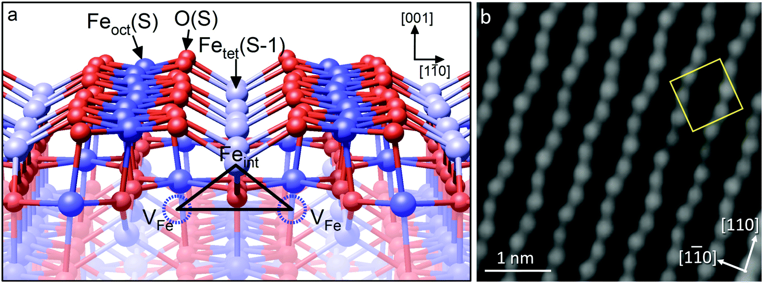 | ||
| Fig. 7 (a) The subsurface cation vacancy (SCV) structure of the reconstructed Fe3O4(001)-(√2 × √2)R45°. In each unit cell, two Feoct atoms in the third layer (labelled VFe) are replaced by an interstitial Fetet atom, labelled Feint, in the second layer. The cation redistribution distorts the otherwise bulk-like surface layer. (b) The distorted rows of Feoct atoms are visible in STM images. The (√2 × √2)R45° unit cell is indicated by the yellow square in the image. Adapted with permission from ref. 43. | ||
The cation-deficient structure at the Fe3O4(001) surface has particularly important consequences for the adsorption of 3d transition metals. For example, Ti, Mn, Co and Ni diffuse into the subsurface at room temperature and occupy Feoct vacancies.43 This behavior is straightforward to understand because such metals form stable ferrite compounds (MexFe3−xO4, Me = metal) based on the spinel structure. The interaction of the Fe3O4(001) surface with molecules is not directly affected by the subsurface vacancies. In fact, the adsorption of organics has many parallels with TiO2(110), due to the close proximity of undercoordinated anion/cation pairs. Formic acid, for example, dissociates on both surfaces to produce formate and hydroxyl groups, but methanol, a weaker acid, does not dissociate on the pristine surface.44 In both cases, methanol reactivity is restricted to point defects. However, whereas VOs are the responsible defects on TiO2(110), the relevant point defects on Fe3O4(001) are excess Fe cations. DFT-based calculations reveal that the energetic cost of accommodating an Fe atom in a two-fold-coordinated adatom geometry is similar to that of incorporating the atom in the subsurface and locally repairing a 2:1 defect cluster of the SCV structure. The adatom is active for adsorption because it is highly undercoordinated, whereas the reparation of the 2:1 defect cluster leads to a Fe3O4-like electronic structure containing Fe2+.
Although DFT+U calculations predict the SCV reconstruction to be energetically favorable across the entire range of oxygen chemical potentials accessible in a UHV experiment, Fe-rich terminations of Fe3O4(001) have been frequently reported.12,45,46 In practice, two main factors determine the amount of excess Fe present at the surface: the sample stoichiometry and the preparation conditions. If the selvedge becomes reduced through the preferential sputtering of O, excess Fe accumulates at the surface. If the annealing temperature is sufficient to allow surface diffusion, yet insufficient to facilitate surface-bulk diffusion and establish defect equilibrium, then metastable, Fe-rich terminations can be formed.
An elegant demonstration of the link between sample stoichiometry and surface termination was recently published by Davis et al.46 In this work, Fe3O4 samples were prepared by evaporating Fe onto a Pt(100) substrate in an O2 partial pressure of ≈5 × 10⁻⁶ mbar. As had been found previously,45 first depositing a buffer layer of Fe(100) avoids the formation of FeO(111) at the Pt interface. This is important because an FeO(111) layer sets the basal plane of the oxide lattice, and enforces growth of an Fe3O4(111) facet. When a buffer layer of 4 nm was used, an Fe3O4(001) surface exhibiting the SCV termination was formed. When 50 nm Fe was used, a well-ordered “Fe-dimer” termination was observed (see Fig. 8). Here two additional Fe atoms are located between the Feoct rows ordered with (√2 × √2) periodicity; the additional Fe donates charge into the surface, which becomes strongly enriched in Fe2+. (While the term “Fe-dimer” is often used in the literature, it is, in fact, a misnomer; the distance between two Fe in a five-fold coordinated, Feoct-like geometry (≈3 Å) is too far for a metal–metal bond.) For Fe buffer layers between 4 nm and 50 nm, several metastable Fe-rich terminations were formed depending on the layer thickness, and the extent of post annealing. The thickness dependence occurs because Fe from the buffer layer diffuses into the Fe3O4 film at the post-annealing temperatures of 700–1020 K, which, given the lack of a semi-infinite bulk, has a significant effect on the sample stoichiometry. The extent of the Fe excess in the film is reflected in the concentration of Fe at the surface.
 | ||
| Fig. 8 An Fe3O4(001) thin film on Pt(100) exhibiting the Fe-dimer termination due to the presence of an Fe(100) buffer layer. (a) Large-scale STM image and (inset) LEED pattern at 95 eV with (√2 × √2)R45° symmetry. (b) High-resolution images show a high density of protrusions ordered with (√2 × √2)R45° symmetry. (inset) In atomically resolved images, the pairs of Fe atoms characteristic of the “Fe-dimer” termination are clearly observed. Reprinted from ref. 46 with permission from Elsevier, copyright 2015. | ||
4. Post-transition metal oxides: In2O3
The oxides of post-transition metals exhibit far fewer polymorphs and cationic oxidation states than those of the d-elements. Their electronic structure, as well as the transport mechanism of excess charge carriers, are also distinctly different from those of transition metal oxides: the more parabolic conduction band gives rise to a low effective mass and high mobility of excess electrons. Again, these materials are often n-doped; reliable p-doping has remained elusive and has hampered the application of, e.g., ZnO in electronic devices. Nevertheless ZnO is heavily used in numerous other applications, including heterogeneous catalysis, and was the subject of many surface studies, see ref. 8 and references therein.The good electrical conductivity that results from the high electron mobility has made post-transition metals ideal candidates for applications where electronics is combined with chemistry, e.g., in chemical sensing. The prototypical gas sensor material is SnO2, and clearly, information about its surface properties can help with understanding the underlying physico-chemical properties; for a review of this material consult ref. 9. The free-electron-like properties of excess charge carriers also imply that polaronic effects are less prominent, and many post-transition metal oxides remain optically transparent even when highly doped. This is a sought-after property for many devices that combine light with electronics, e.g., in solar cells or LEDs. The prototypical transparent conducting oxide (TCO) is indium oxide, In2O3, usually doped with Sn and then referred to as ITO.
Coming back to intrinsic point defects, recent studies clearly show how reducing conditions affect the surface structure of In2O3(111).47,48 (For a recent review on the surfaces of In2O3 and ITO, see the work by Edgell.23) The non-polar In2O3(111) surface is the thermodynamically most stable facet of this material. A (1 × 1) surface with a relaxed, bulk-terminated structure results when an In2O3 single crystal is oxidized under UHV conditions, see the left side of Fig. 9d.
 | ||
| Fig. 9 Comparison of stoichiometric and reduced In2O3(111). (a1) Empty-states STM images of the stoichiometric surface, which is essentially a simple truncation of the bulk; the (1 × 1) unit cell is marked in white. (a2) STM images of the reduced surface, which is characterized by single In adatoms. Each of these adatoms sits at one specific site in the unit cell, in the middle of the triangles marked in yellow. (b1) Height profile along a high-symmetry direction of the stoichiometric surface across a single-layer step of 290 pm. (b2) Height profile across several In adatoms of the reduced surface. (c1 and c2) Calculated STM images of the stoichiometric and reduced surfaces, respectively. (d) Atomic model of the relaxed bulk termination (left) and reduced surface (right). (Reprinted from ref. 47 with permission from John Wiley and Sons, copyright 2014). | ||
The panels in Fig. 9a and b show STM images of In2O3(111), prepared in stoichiometric and reduced form by annealing at 450 °C in ∼5 × 10⁻⁷ mbar O2 and in UHV, respectively. In early DFT calculations,49 VOs have been considered; it is easiest to remove the O3c atoms surrounding the In6c on the surface (shaded as light red and blue balls in Fig. 9d, respectively). However, surface VOs have not been observed in SPM. As seen in Fig. 9b, a surface with single In adatoms forms instead. These adatoms assume specific positions in the unit cell: referring to the model in Fig. 9d they are located at position ‘B’ on top of the region with the O3c atoms, which appears as a dark depression in STM images of the stoichiometric surface (marked by yellow triangles in Fig. 9). The preferred location for the excess In gives rise to a remarkably well-ordered adatom array that covers the whole surface. The adatom formation is reversible; upon heating in O2 at elevated temperatures the In atoms react with the oxygen and form small, stoichiometric In2O3 islands. The propensity for adatom formation is in excellent agreement with more recent DFT calculations,47 which confirm that an In-rich surface is energetically most favorable over wide range of O chemical potentials, and where the STM contrast is quantitatively reproduced (see Fig. 9c). According to these DFT results, very low O chemical potentials never result in VO formation but favor In dimers and trimers. This is also observed in STM images after annealing to higher temperatures, where small clusters of adatoms start to appear in the dark triangles.
Interestingly, the In-adatom surface also forms when the system interacts with a reactive metal.48 Vapor deposition of small amounts of Fe at room temperature on the stoichiometric In2O3(111) surface leads to adatoms; in STM these show an identical appearance and height to the adatoms that form by thermal reduction. DFT calculations show a clear preference for Fe to be incorporated into the topmost In2O3 layer, where it replaces an In that then moves as an adatom to the surface. Such a process can be viewed as a solid-state redox reaction, where the incorporated Fe is oxidized to Fe3+ (the same oxidation state as In), but reduces the In atom. It has been argued48 that the reason for expelling the excess In atom to the surface rather than keeping it subsurface as interstitials is related to the differences between the ionic and neutral radii of the atoms. Moreover, Fe2O3 is more stable then In2O3 and the reaction is exothermic.
The behavior of reduced In2O3 has parallels to the one observed for iron-rich Fe3O4; in both cases excess metal atoms appear on the surface, and are located at specific sites in the unit cell (compare Fig. 8 and 9). While for the iron oxides there is a clear relation to the bulk (where, as pointed out above, cation vacancies govern the structural transitions between the different iron oxide polymorphs), VOs are generally considered as defects in the reducing regime for intrinsic and doped In2O3;50 the cubic bixbyite structure of In2O3 is essentially a flourite-type lattice with ordered VOs. The In-adatom phase observed with STM in Fig. 9 is thus quite surprising, and a shining example how STM studies can help obtaining a more truthful picture of the defect chemistry of oxides.
5. Conclusion and outlook
As this short review shows, the direct study of point defects with SPM techniques has made great strides in recent decades. The concepts of defect equilibria, established with macroscopic techniques, are now supplemented and enhanced by microscopic insights that stem from such surface science experiments. For example oxygen vacancies, a key concept in catalysis and solid-state chemistry, can be directly inspected and even manipulated with SPM techniques, and their effect on relevant catalytic processes can be evaluated in a rather direct manner. This is a prime example of how distinct fields of science can learn from each other. Such interdisciplinary exchange will be even more important in the future as we search for appropriate materials for more energy-efficient catalysts and energy conversion schemes. In this context, it is worth pointing out that the atom-by-atom control exemplified here has only been established for a relatively small set of binary oxides. Little work is available on point defects on very promising materials such as, e.g., ternary oxides in the form of perovskites or spinels. Here surface structures are more complex and adapt strongly to changes in stoichiometry, which makes the identification of atomic-sized defects quite challenging. On the other hand the ease of doping and the richness in their electronic properties makes these materials prime candidates for energy-related applications.Wide-band-gap insulators are another class of materials that provides fertile ground for future investigations. Here the application of surface science techniques to bulk single crystals has been particularly challenging. With the progress in high-resolution AFM measurements, studies of point defects are now possible on true insulators, and it will be interesting to compare results from bulk materials with those obtained on the ultrathin films that have long served as surface science model systems. AFM also opens up opportunities for exciting new investigations, such as a more direct view of O surface atom configurations, the dis-entanglement of the electronic and geometric structure, measurement of the local surface potential, and the determination of charge states of adsorbates or impurities.
As shown in the last example, i.e., the unexpected observation of excess In adatoms on the In2O3(111) surface under reducing conditions, there is ample space for surprises when it comes to surface structures on oxides. This is particularly important as expanding capabilities in theory allow more efficient calculations and a systematic screening of materials properties using computations – such efforts are only useful when the defect configurations that are assumed are indeed the ones that manifest themselves in nature. The interplay of well-established concepts, progress in computational materials science, and advancements in direct, atomically resolved experimental measurements, we will let us dive ever deeper into the mysteries of these fascinating materials that make out so much of our natural and technological world.
Acknowledgements
The authors gratefully acknowledge funding through projects from the Austrian Science Fund FWF (Wittgenstein-Prize Z 250-N27 (UD & MaS); START-Prize Y 847-N20 (GSP); Herta-Firnberg Grant T 749-N27 (MW); Special Research Project ‘Functional Surfaces and Interfaces, FOXSI F4507-N16 (MiS & UD)) and the European Research Council (UD: ERC-2011-ADG_20110209 Advanced Grant ‘OxideSurfaces’).References
- H. L. Tuller and S. R. Bishop, Point defects in oxides: tailoring materials through defect engineering, Annu. Rev. Mater. Res., 2011, 41(1), 369–398 CrossRef CAS.
- V. E. Henrich and P. A. Cox, The surface science of metal oxides, Cambridge University Press, 1994 Search PubMed.
- C. T. Campbell and J. Sauer, Introduction: surface chemistry of oxides, Chem. Rev., 2013, 113(6), 3859–3862 CrossRef CAS PubMed.
- U. Diebold, S.-C. Li and M. Schmid, Oxide surface science, Annu. Rev. Phys. Chem., 2010, 61(1), 129–148 CrossRef CAS PubMed.
- U. Diebold, The surface science of titanium dioxide, Surf. Sci. Rep., 2003, 48(5–8), 53–229 CrossRef CAS.
- Z. Dohnálek, I. Lyubinetsky and R. Rousseau, Thermally-driven processes on rutile TiO2(110)-(1 × 1): a direct view at the atomic scale, Prog. Surf. Sci., 2010, 85(5–8), 161–205 CrossRef.
- C. L. Pang, R. Lindsay and G. Thornton, Structure of clean and adsorbate-covered single-crystal rutile TiO2 surfaces, Chem. Rev., 2013, 113(6), 3887–3948 CrossRef CAS PubMed.
- C. Wöll, The chemistry and physics of zinc oxide surfaces, Prog. Surf. Sci., 2007, 82(2–3), 55–120 CrossRef.
- M. Batzill and U. Diebold, The surface and materials science of tin oxide, Prog. Surf. Sci., 2005, 79(2–4), 47–154 CrossRef CAS.
- D. R. Mullins, The surface chemistry of cerium oxide, Surf. Sci. Rep., 2015, 70(1), 42–85 CrossRef CAS.
- S. Surnev, M. Ramsey and F. Netzer, Vanadium oxide surface studies, Prog. Surf. Sci., 2003, 73(4–8), 117–165 CrossRef CAS.
- G. S. Parkinson, Iron oxide surfaces, Surf. Sci. Rep., 2016, 71(1), 272–365 CrossRef CAS.
- J. Jupille and G. Thornton, Defects at Oxide Surfaces. Springer International Publishing, Cham, 2015, vol. 58 Search PubMed.
- F. J. Giessibl, Principles and Applications of the qPlus Sensor, Springer Berlin Heidelberg, Berlin, Heidelberg, 2009, pp. 121–142 Search PubMed.
- L. Gross, Recent advances in submolecular resolution with scanning probe microscopy, Nat. Chem., 2011, 3(4), 273–278 CrossRef CAS PubMed.
- J. Lauritsen and M. Reichling, Atomic resolution non-contact atomic force microscopy of clean metal oxide surfaces, J. Phys.: Condens. Matter, 2010, 22, 263001 CrossRef CAS PubMed.
- K. Katsiev, A. Kolmakov, M. Fang and U. Diebold, Characterization of individual SnO2 nanobelts with STM, Surf. Sci., 2008, 602(14), 112–114 CrossRef.
- C. Noguera, Polar oxide surfaces, J. Phys.: Condens. Matter, 2000, 12(31), R367–R410 CrossRef CAS.
- I. G. Austin and N. F. Mott, Polarons in crystalline and non-crystalline materials, Adv. Phys., 2001, 50(7), 757–812 CrossRef.
- C. M. Yim, M. B. Watkins, M. J. Wolf, C. L. Pang, K. Hermansson and G. Thornton, Engineering polarons at a metal oxide surface, Phys. Rev. Lett., 2016, 117(11), 116402 CrossRef CAS PubMed.
- M. Setvín, C. Franchini, X. Hao, M. Schmid, A. Janotti, M. Kaltak, C. G. Van de Walle, G. Kresse and U. Diebold, Direct view at excess electrons in TiO2 rutile and anatase, Phys. Rev. Lett., 2014, 113(8), 086402 CrossRef PubMed.
- S. Shaikhutdinov and H.-J. Freund, Ultrathin oxide films on metal supports: structure–reactivity relations, Annu. Rev. Phys. Chem., 2012, 63(1), 619–633 CrossRef CAS PubMed.
- R. G. Egdell, Dopant and Defect Induced Electronic States at In2O3 Surfaces, Springer International Publishing, Cham, 2015, vol. 58, pp. 351–400 Search PubMed.
- J. Nowotny, T. Norby and T. Bak, Reactivity between titanium dioxide and water at elevated temperatures, J. Phys. Chem. C, 2010, 114, 18215–18221 CAS.
- M. Li, W. Hebenstreit, U. Diebold, A. M. Tyryshkin, M. K. Bowman, G. G. Dunham and M. A. Henderson, The influence of the bulk reduction state on the surface structure and morphology of rutile TiO2(110) single crystals, J. Phys. Chem. B, 2000, 104(20), 4944–4950 CrossRef CAS.
- R. Moos and K. H. Hardtl, Defect chemistry of donor-doped and undoped strontium titanate ceramics between 1000 degrees and 1400 degrees C, J. Am. Ceram. Soc., 1997, 80(10), 2549–2562 CrossRef CAS.
- M. Aono and R. R. Hasiguti, Interaction and ordering of lattice-defects in oxygen-deficient rutile TiO2−x, Phys. Rev. B: Condens. Matter Mater. Phys., 1993, 48(17), 12406–12414 CrossRef CAS.
- S. Wendt, P. T. Sprunger, E. Lira, G. K. H. Madsen, Z. Li, J. O. Hansen, J. Matthiesen, A. Blekinge-Rasmussen, E. Laegsgaard, B. Hammer and F. Besenbacher, The role of interstitial sites in the Ti3d defect state in the band gap of titania, Science, 2008, 320(5884), 1755–1759 CrossRef CAS PubMed.
- T. Minato, Y. Sainoo, Y. Kim, H. Kato, K. Aika, M. Kawai, J. Zhao, H. Petek, T. Huang and W. He, The electronic structure of oxygen atom vacancy and hydroxyl impurity defects on titanium dioxide (110) surface, J. Chem. Phys., 2009, 130, 124502 CrossRef PubMed.
- P. Krüger, S. Bourgeois, B. Domenichini, H. Magnan, D. Chandesris, P. Le Fèvre, A. M. Flank, J. Jupille, L. Floreano, A. Cossaro, A. Verdini and A. Morgante, Defect States at the TiO2(110) Surface Probed by Resonant Photoelectron Diffraction, Phys. Rev. Lett., 2008, 100(5), 1–4 CrossRef PubMed.
- F. Esch, Electron localization determines defect formation on ceria substrates, Science, 2005, 309(5735), 752–755 CrossRef CAS PubMed.
- J. Kullgren, M. J. Wolf, C. W. M. Castleton, P. Mitev, W. J. Briels and K. Hermansson, Oxygen vacancies versus fluorine at CeO2(111): a case of mistaken identity?, Phys. Rev. Lett., 2014, 112(15), 156102 CrossRef CAS PubMed.
- Y. Sugimoto, P. Pou, M. Abe, P. Jelínek, R. Pérez, S. Morita and Ó. Custance, Chemical identification of individual surface atoms by atomic force microscopy, Nature, 2007, 446(7131), 64–67 CrossRef CAS PubMed.
- L. Gross, F. Mohn, P. Liljeroth, J. Repp, F. J. Giessibl and G. Meyer, Measuring the charge state of an adatom with noncontact atomic force microscopy, Science, 2009, 324(5933), 1428–1431 CrossRef CAS PubMed.
- R. Bechstein, C. González, J. Schütte, P. Jelínek and R. Pérez, “All-inclusive” imaging of the rutile TiO2(110) surface using NC-AFM, Nanotechnology, 2009, 20, 505703 CrossRef PubMed.
- R. Waser, R. Dittmann, G. Staikov and K. Szot, Redox-based resistive switching memories – nanoionic mechanisms, prospects, and challenges, Adv. Mater., 2009, 21(25–26), 2632–2663 CrossRef CAS.
- M. Setvín, X. Hao, B. Daniel, J. Pavelec, Z. Novotný, G. S. Parkinson, M. Schmid, G. Kresse, C. Franchini and U. Diebold, Charge trapping at the step edges of TiO2 anatase (101), Angew. Chem., Int. Ed., 2014, 53(18), 4714–4716 CrossRef PubMed.
- M. Setvin, U. Aschauer, P. Scheiber, Y. F. Li, W. Hou, M. Schmid, A. Selloni and U. Diebold, Reaction of O2 with subsurface oxygen vacancies on TiO2 anatase(101), Science, 2013, 341(6149), 988–991 CrossRef CAS PubMed.
- M. Setvín, M. Schmid and U. Diebold, Aggregation and electronically induced migration of oxygen vacancies in TiO2 anatase, Phys. Rev. B: Condens. Matter Mater. Phys., 2015, 91, 195403 CrossRef.
- G. Ketteler, W. Weiss, W. Ranke and R. Schlögl, Bulk and surface phases of iron oxides in an oxygen and water atmosphere at low pressure, Phys. Chem. Chem. Phys., 2001, 3(6), 1114–1122 RSC.
- I. Bernal-Villamil and S. Gallego, Electronic structure and polaronic charge distributions of Fe vacancy clusters in Fe1−xO, Phys. Rev. B: Condens. Matter Mater. Phys., 2014, 90(19), 195126 CrossRef.
- R. Bliem, E. McDermott, P. Ferstl, M. Setvín, O. Gamba, J. Pavelec, M. A. Schneider, M. Schmid, U. Diebold, P. Blaha, L. Hammer and G. S. Parkinson, Subsurface cation vacancy stabilization of the magnetite (001) surface, Science, 2014, 346(6214), 1212–1215 CrossRef PubMed.
- R. Bliem, J. Pavelec, O. Gamba, E. McDermott, Z. Wang, S. Gerhold, M. Wagner, J. Osiecki, K. Schulte, M. Schmid, P. Blaha, U. Diebold and G. S. Parkinson, Adsorption and incorporation of transition metals at the magnetite Fe3O4(001) surface, Phys. Rev. B, 2015, 92(7), 075440 CrossRef.
- O. Gamba, H. Noei, J. Pavelec, R. Bliem, M. Schmid, U. Diebold, A. Stierle and G. S. Parkinson, Adsorption of formic acid on the Fe3O4(001) surface, J. Phys. Chem. C, 2015, 119(35), 20459–20465 CAS.
- N. Spiridis, J. Barbasz, Z. Łodziana and J. Korecki, Fe3O4(001) films on Fe(001): termination and reconstruction of iron-rich surfaces, Phys. Rev. B: Condens. Matter Mater. Phys., 2006, 74(15), 155423 CrossRef.
- E. M. Davis, K. Zhang, Y. Cui, H. Kuhlenbeck, S. Shaikhutdinov and H.-J. Freund, Growth of Fe3O4(001) thin films on Pt(100): tuning surface termination with an Fe buffer layer, Surf. Sci., 2015, 636(C), 42–46 CrossRef CAS.
- M. Wagner, S. Seiler, B. Meyer, L. A. Boatner, M. Schmid and U. Diebold, Reducing the In2O3(111) surface results in ordered indium adatoms, Adv. Mater. Interfaces, 2014, 1(8), 1400289 CrossRef.
- M. Wagner, P. Lackner, S. Seiler, S. Gerhold, J. Osiecki, K. Schulte, L. A. Boatner, M. Schmid, B. Meyer and U. Diebold, Well-ordered In adatoms at the In2O3(111) surface created by Fe deposition, Phys. Rev. Lett., 2016, 117(20), 206101 CrossRef PubMed.
- P. Agoston and K. Albe, Thermodynamic stability, stoichiometry, and electronic structure of bcc In2O3 surfaces, Phys. Rev. B: Condens. Matter Mater. Phys., 2011, 84, 045311 CrossRef.
- S. Harvey, T. Mason, Y. Gassenbauer, R. Schafranek and A. Klein, Surface versus bulk electronic/defect structures of transparent conducting oxides: I. Indium oxide and ITO, J. Phys. D: Appl. Phys., 2006, 39(18), 3959–3968 CrossRef CAS.
Footnotes |
† Throughout this article we adopt the Kröger–Vink notation, where the main character stands for the type of species considered, and the subscript its position in the lattice, e.g. a vacancy at an oxygen site is called VO, and a metal at an interstitial site is called Mi. The superscripts ˙ and ′ indicate nominal positive and negative charges, respectively. This formal oxidation state is given as compared to the undisturbed lattice; i.e., an O vacancy site where no electrons are localized is denoted as  . . |
| ‡ Here ‘macroscopic’ is more of a practical term. It means that the crystals need to be at least ≈1 mm in size, although is also possible to conduct STM imaging of nanomaterials under certain conditions.17 |
| § We note that re-oxidation of a strongly-reduced TiO2 crystal in air likely also introduces nitrogen into the lattice. Further, a temperature of ∼1000 K would be sufficient for re-oxidation. |
| ¶ It needs to be emphasized that the density of defects in the bulk27 is much smaller, typically in the range of 10−4. |
| This journal is © The Royal Society of Chemistry 2017 |