
 Open Access Article
 This Open Access Article is licensed under a
 Creative Commons Attribution 3.0 Unported Licence
Photoelectrochemical devices for solar water splitting – materials and challenges†
Chaoran
Jiang
 ab,
Savio J. A.
Moniz
a,
Aiqin
Wang
b,
Tao
Zhang
b and
Junwang
Tang
*a
ab,
Savio J. A.
Moniz
a,
Aiqin
Wang
b,
Tao
Zhang
b and
Junwang
Tang
*a
aDepartment of Chemical Engineering, University College London, Torrington Place, London, WC1E 7JE, UK. E-mail: Junwang.tang@ucl.ac.uk
bState Key Laboratory of Catalysis, Dalian Institute of Chemical Physics, Chinese Academy of Sciences, Dalian, 116023, China
First published on 23rd June 2017
Abstract
It is widely accepted within the community that to achieve a sustainable society with an energy mix primarily based on solar energy we need an efficient strategy to convert and store sunlight into chemical fuels. A photoelectrochemical (PEC) device would therefore play a key role in offering the possibility of carbon-neutral solar fuel production through artificial photosynthesis. The past five years have seen a surge in the development of promising semiconductor materials. In addition, low-cost earth-abundant co-catalysts are ubiquitous in their employment in water splitting cells due to the sluggish kinetics of the oxygen evolution reaction (OER). This review commences with a fundamental understanding of semiconductor properties and charge transfer processes in a PEC device. We then describe various configurations of PEC devices, including single light-absorber cells and multi light-absorber devices (PEC, PV-PEC and PV/electrolyser tandem cell). Recent progress on both photoelectrode materials (light absorbers) and electrocatalysts is summarized, and important factors which dominate photoelectrode performance, including light absorption, charge separation and transport, surface chemical reaction rate and the stability of the photoanode, are discussed. Controlling semiconductor properties is the primary concern in developing materials for solar water splitting. Accordingly, strategies to address the challenges for materials development in this area, such as the adoption of smart architectures, innovative device configuration design, co-catalyst loading, and surface protection layer deposition, are outlined throughout the text, to deliver a highly efficient and stable PEC device for water splitting.
 Chaoran Jiang | Chaoran Jiang obtained his BSc degree in Chemistry from Northern Arizona University (USA) in 2012. After studying for a one-year MSc in Chemical Process Engineering at UCL, he became a PhD research student in the Solar Energy & Advanced Materials Research Group at UCL under the supervision of Dr Junwang Tang in 2013. He is currently in Dalian Institute of Chemical Physics (DICP) as an exchange student. His current research focuses on semiconductor photoelectrochemistry for solar water splitting. |
 Savio J. A. Moniz | Dr Savio J. A. Moniz is a post-doctoral research associate working under the supervision of Junwang Tang in the Solar Energy & Advanced Materials Group at UCL. Prior to this, he gained his PhD in Inorganic Chemistry at UCL Chemistry Department under Chris Blackman and Claire Carmalt, working on MOCVD of multiferroic oxides for solar energy harvesting and NVRAM. His current research focuses on the fabrication and mechanistic aspects of photocatalysts for solar fuels synthesis. |
 Aiqin Wang | Dr Aiqin Wang is a professor at the Dalian Institute of Chemical Physics (DICP). She received her PhD degree in physical chemistry from DICP in 2001. After two years as a postdoctoral fellow in National Taiwan University, she returned to DICP in 2005 and joined Prof. Tao Zhang's group where she was promoted to a full professor in 2009. Her current research interests involve sub-nanometer and single-atom catalysts, catalytic conversion of biomass, green synthesis of fine chemicals, and C1 chemistry. |
 Tao Zhang | Prof. Tao Zhang received his PhD degree in 1989 from Dalian Institute of Chemical Physics (DICP). After one year at the University of Birmingham as a post-doctoral fellow, he joined DICP again in 1990 where he was promoted to a full professor in 1995. He is currently the Director of DICP. He also serves as the Editor-in-Chief of the Chinese Journal of Catalysis, and serves as an Editorial Board Member of Applied Catalysis B and an Advisory Board Member of ChemPhysChem. His research interests focus on the catalytic conversion of biomass, design and synthesis of single-atom catalysts, and environmental catalysis. |
 Junwang Tang | Dr Junwang Tang is the Director of UCL Materials Hub and Professor of Materials Chemistry in the Department of Chemical Engineering at UCL. He obtained his PhD in Physical Chemistry in 2001. After that, he was appointed as a JSPS Fellow at NIMS, Japan and a senior researcher in the Department of Chemistry at Imperial College London, working on solar fuels synthesis and mechanistic studies by time-resolved spectroscopies. After that, he took a faculty position at UCL. His current research interests lie in photocatalytic CH4 transformation, ammonia synthesis, solar water splitting, CO2 conversion by artificial photosynthesis and mechanistic aspects of solar energy conversion, and water treatment, as well as microwave-assisted intensified flow chemistry. He is also a Fellow of the RSC. |
Key learning points(1) Fundamental aspects of semiconductor physics and the behaviour of photoexcited carriers during photoelectrochemical water splitting processes.(2) Design concept of different configurations in an efficient PEC device and criteria for evaluating the photoelectrochemical water splitting performance. (3) The most important photoanode/photocathode materials developed to date (e.g. TiO2, BiVO4, Fe2O3, CdS, Cu2O, Si and III–V materials). (4) The most important earth-abundant co-catalyst/electrocatalysts developed recently. (5) Combination strategies, including material doping, the adoption of smart architectures, innovative device configuration design, co-catalysts loading and surface modification for highly efficient and stable photoelectrodes. |
1. Introduction
Solar energy is the most abundant, clean and renewable energy resource on the planet. Each year, the amount of solar energy reaching our planet is approximately 100![[thin space (1/6-em)]](https://www.rsc.org/images/entities/char_2009.gif) 000 TW, of which approximately 36000 TW reaches the land. This means that only 1% of the land on Earth needs to be covered with just 10%-efficient photoelectrochemical (PEC) cells to generate the equivalent of 36 TW per year, which is sufficient to satisfy predicted global annual energy consumption in the year 2050.1 Hence, the ability to harness and utilize solar energy is of great importance. Artificial photosynthesis is a promising technology not only to harvest solar energy but also as a means of storage, in producing energy-rich chemical fuels such as hydrogen or hydrocarbons via processes such as water splitting or CO2 utilisation. Among the various chemical fuels, hydrogen exhibits 3–4 fold higher mass energy density compared to gasoline and can be utilised either through direct combustion or in hydrogen fuel cells. However, it remains a significant challenge to construct an adequately efficient and stable solar-to-hydrogen (STH) energy conversion device. Even though water splitting devices have recently been reported to operate with an STH efficiency of 30% through coupling a photovoltaic cell and an electrolyser,2 research is now concentrated on the development of direct low-cost, highly stable water splitting using PEC cells. This is due to two major driving forces. Firstly, a low overpotential is needed to drive the PEC water splitting, promising a higher STH conversion efficiency, despite the fact that several PV cells are usually used in series in order to reach the minimum potential (3.0 V required by the electrolyser in an indirect route). Secondly, PEC water splitting requires a much simpler and space-saving construction with fewer components (wires, electrodes, reactor, etc.); thus the cost of the PV–electrolyser system is estimated to be at least US $8 per kg, but can be reduced to ca. US $3 per kg by integrating both a light harvester and a water splitting photocatalyst in a single system (PEC cell). Such a system has the potential to produce H2 at the target price of US $2–4 per kg set by the US Department of Energy (DOE) in order to be commercially viable and competitive with steam reforming. This review will thus place an emphasis on the fundamental aspects of PEC water splitting and recent developments on the optimisation of PEC device configuration. First, the principles of semiconductor band bending and PEC water splitting processes will be described. Secondly, various PEC device configurations will be presented, along with technical remarks. Finally, some promising materials for PEC devices will be covered and strategies to improve their performance will be discussed, with the aim of directing research into these areas.
000 TW, of which approximately 36000 TW reaches the land. This means that only 1% of the land on Earth needs to be covered with just 10%-efficient photoelectrochemical (PEC) cells to generate the equivalent of 36 TW per year, which is sufficient to satisfy predicted global annual energy consumption in the year 2050.1 Hence, the ability to harness and utilize solar energy is of great importance. Artificial photosynthesis is a promising technology not only to harvest solar energy but also as a means of storage, in producing energy-rich chemical fuels such as hydrogen or hydrocarbons via processes such as water splitting or CO2 utilisation. Among the various chemical fuels, hydrogen exhibits 3–4 fold higher mass energy density compared to gasoline and can be utilised either through direct combustion or in hydrogen fuel cells. However, it remains a significant challenge to construct an adequately efficient and stable solar-to-hydrogen (STH) energy conversion device. Even though water splitting devices have recently been reported to operate with an STH efficiency of 30% through coupling a photovoltaic cell and an electrolyser,2 research is now concentrated on the development of direct low-cost, highly stable water splitting using PEC cells. This is due to two major driving forces. Firstly, a low overpotential is needed to drive the PEC water splitting, promising a higher STH conversion efficiency, despite the fact that several PV cells are usually used in series in order to reach the minimum potential (3.0 V required by the electrolyser in an indirect route). Secondly, PEC water splitting requires a much simpler and space-saving construction with fewer components (wires, electrodes, reactor, etc.); thus the cost of the PV–electrolyser system is estimated to be at least US $8 per kg, but can be reduced to ca. US $3 per kg by integrating both a light harvester and a water splitting photocatalyst in a single system (PEC cell). Such a system has the potential to produce H2 at the target price of US $2–4 per kg set by the US Department of Energy (DOE) in order to be commercially viable and competitive with steam reforming. This review will thus place an emphasis on the fundamental aspects of PEC water splitting and recent developments on the optimisation of PEC device configuration. First, the principles of semiconductor band bending and PEC water splitting processes will be described. Secondly, various PEC device configurations will be presented, along with technical remarks. Finally, some promising materials for PEC devices will be covered and strategies to improve their performance will be discussed, with the aim of directing research into these areas.
2. Principle of PEC water splitting
The main components of PEC water splitting devices are the semiconductor light absorbing photoelectrodes, the electrolyte and the separation membrane. In this section, the basic properties of semiconductors will be discussed, followed by a description of the semiconductor–electrolyte interface. Finally, the basic processes and mechanism of PEC water splitting will be described.2.1 Semiconductors
According to molecular bonding theory, bonding and anti-bonding levels are formed by the combination of atomic orbitals of several atoms. The closed sets of energy levels constitute a region called energy bands. The valence band (highest occupied molecular orbital, HOMO) and conduction band (lowest unoccupied molecular orbital, LUMO) are formed, which correspond to the bonding and anti-bonding energy levels, respectively. The difference between the two energy levels is termed the band-gap (Eg) and the band-gap of semiconductors is usually in the range of 1–5 eV. At zero kelvin, the valence band is filled with electrons, whereas the conduction band is mostly empty. Upon excitation by an external energy source (e.g. a photon), charge-carriers are generated and an electron in the valence band is excited to the conduction band, leaving a hole in the valence band. These photogenerated electron–hole pairs play a crucial role in water splitting reactions, and will be discussed in more detail in Section 2.2. Since pure semiconductors (intrinsic semiconductors) exhibit poor conductivity, they are usually doped with impurity atoms (termed extrinsic semiconductors) as either electron donors or acceptors. As illustrated in Fig. 1, the donor-doped semiconductors (e.g. phosphorus into Si) have impurity atoms with a greater number of valence electrons than the host atom, resulting in an electron-rich semiconductor (n-type), whilst acceptor-doped semiconductors have impurity atoms with fewer valence electrons than the host atom, resulting in hole-rich semiconductors (p-type). For an n-type semiconductor, the majority carriers are electrons, whereas in p-type semiconductors these are the holes. | ||
| Fig. 1 Schematic bond representation for (a) intrinsic silicon; (b) n-type silicon doped with phosphorus and (c) p-type silicon doped with boron. | ||
In metal oxide photoelectrodes, shallow donors and acceptors are almost always necessary because of the low intrinsic charge carrier mobilities. Not only can conductivity be improved, but also optical absorption, carrier diffusion length and catalytic activity. Defects such as vacancies, interstitials or substituents are also usually present in the materials, and the incorporation of dopants into metal oxides and other ionic materials can be described using the Kroger–Fink notation, which represents the overall defect chemistry of the material from the viewpoint of conserving lattice site stoichiometry.3 For more details on the Kroger–Fink notation, readers are directed to the textbook by D. Smyth.4 A typical example of beneficial doping of compound semiconductors for water splitting is that of Ta-doped α-Fe2O3. Here, Ta5+ substitutes for Fe3+, giving two positive charges at each substituted site. Two electrons are added to conserve the overall charge; doping with Ta increases the electron density in α-Fe2O3. The resultant doped material displays remarkably improved photoactivity at 420 nm compared to the undoped sample. The overall equation [where the mole ratio of Ta:Fe in the Ta-doped haematite is x/(1 − x)] using an iron(III) nitrate precursor is as follows:5

There are many more examples of doping of ternary oxides and more complex oxides; however, these fall outside the scope of this Tutorial Review. Readers are directed toward the excellent text from Van de Krol for further examples of material and doping types.3
2.2 Semiconductor band-bending and the space charge region
When a semiconductor is immersed in an electrolyte, the electrochemical potential (Fermi level) is disparate across the interface. Equilibration of this interface requires the flow of charge from one phase to the other, and a “band bending” takes place within the semiconductor. At the semiconductor–liquid junction (SCLJ), the equilibration of the chemical potential of the electrons in the semiconductor (Fermi level) and the oxidation–reduction potential in the electrolyte causes the transfer of electrons across the SCLJ. There is also a characteristic region within the semiconductor within which the charge would have been removed by this equilibration process. Beyond this, the semiconductor is electrically neutral, so therefore this layer is termed the space charge region (SCR) or depletion layer, because the layer is depleted of the majority carriers.6 One of the key characteristics of a semiconductor used for PEC water splitting is the presence of a built-in electric field in the SCR, where band bending takes place. In devices for solar water splitting, this SCR and the subsequent band bending aid the transfer and separation of the photogenerated electrons and holes, and therefore are of great importance to understanding the different types of band bending exhibited in PEC systems.Yates et al. have reviewed the phenomena of band bending in semiconductors and the resultant effects on photochemistry, particularly with respect to photogenerated charge separation and transport.7 Band bending can be induced by metal/semiconductor contact, surface state, applied bias and molecule absorption, which result in the formation of a space charge region. In this section, different types of band bending will be discussed in detail.
 | ||
| Fig. 2 Energy band diagrams of metal and n-type semiconductor contacts, where Evac = vacuum energy; Ec = energy of conduction band minimum; Ev = energy of valence band maximum; Ef(m) = Fermi level of metal; Ef(s) = Fermi level of semiconductor; ϕm = metal work function; ϕs = semiconductor work function; VBB = degree of band bending of the semiconductor at the interface. Modified from ref. 7 with permission from the American Chemical Society. In the energy band diagram of the metal in contact with a p-type semiconductor, the band bending reverses. | ||
 | ||
| Fig. 3 Schematic illustration of surface-state induced band bending: (a) disequilibrium and equilibrium between the bulk and the surface for an n-type semiconductor; (b) disequilibrium and equilibrium between the bulk and the surface for a p-type semiconductor; modified from ref. 7 with permission from the American Chemical Society. | ||
 | ||
| Fig. 4 Schematic diagram shows the adsorption of an acceptor molecule (A) onto a semiconductor surface. Modified from ref. 7 with permission of the American Chemical Society. | ||
 | ||
| Fig. 5 Effect of applying a bias voltage (VA) to an n-type semiconductor photoelectrode. VH is the potential drop across the Helmholtz layer. Φm is the work function of the metal. Φsc is the potential drop across the space charge region. Reproduced from ref. 3 with permission of Springer Science+Business Media, LLC. | ||
 | ||
| Fig. 6 The band energetics of an n-type semiconductor/electrolyte contact showing the relationships between the electrolyte redox couple (H2O/O2 and H2/H+), the Helmholtz layer potential drop (VH), and the semiconductor work function (Φs), the electrolyte work function (ΦR), the electron quasi-Fermi level (EF,n) and hole quasi-Fermi level (EF,p) in three cases: (A) before equilibration between the two phases; (B) after equilibration under dark conditions; and (C) in quasi-static equilibrium under steady-state illumination. The voltage (VOC) generated by the junction under illumination is given by the difference between EF,n and the electrochemical potential of the redox couple of interest (H2O/O2 for an n-type semiconductor and H2/H+ for a p-type). | ||
2.3 PEC water splitting processes
The water splitting reaction is an uphill reaction, which requires a minimum Gibbs free energy of 237 kJ mol−1. As shown in Fig. 7, there are three major physiochemical processes that are involved in a complete PEC water splitting reaction. The first process is light absorption from a calibrated light source (e.g. simulated one sun irradiation, 100 mW cm−2 is often used) by the semiconducting photoelectrode, usually with an n-type semiconductor as the anode and a p-type semiconductor as the cathode. When a semiconductor absorbs photons with energies greater than its band gap energy (Eg), a pair of charge carriers is created: electrons are excited to the conduction band, leaving holes in the valence band (VB). The valence band potential must be more positive than the O2/H2O redox potential of 1.23 V vs. NHE (pH = 0) to permit water oxidation, whilst the conduction band (CB) must be more negative than the H+/H2 redox potential of 0 V vs. NHE to carry out water reduction. Note that additional overpotential is required due to the energy losses associated with the photoholes passing through the space charge region and electrons transferring through the external circuit to the counter electrode (e.g. platinum). The second process is the separation and transportation of photogenerated electron–hole pairs. During these steps, charge carriers can either recombine in the bulk or at the surface, and hence both efficient separation and high mobility of charge carriers are desirable. The last process is the surface reaction where the redox reactions for water splitting occur. Both the potential of the charge carriers and suitable reaction kinetics are crucial for efficient water splitting. | ||
| Fig. 7 Schematic diagram of a simple PEC cell based on an n-type semiconducting photoanode electrically connected to a metal counter electrode under an external bias, performed in alkaline conditions. On the photoanode, 4OH− + 4H+ → 2H2O + O2 takes place and a bias is required, as the position of CB is too positive to also drive water reduction. The main processes involve: (I) light absorption; (II) charge carrier separation and transportation and (III) surface redox reactions. | ||
2.4 Energy and quantum conversion efficiencies
The energy conversion efficiency is the ultimate performance indicator of a PEC cell.The standard solar-to-hydrogen conversion efficiency (ηSTH) can be expressed as the ratio between the total energy generated and the total energy input from sunlight irradiation (AM 1.5G, 100 mW cm−2):

When an external bias is applied to the PEC system, the electrical energy must be subtracted and thus the applied bias photon-to-current efficiency (ABPE) is frequently used:

Determination of Faradaic efficiency is the most useful method to verify that the generated photocurrent is in fact due to water splitting and not photocorrosion of the electrodes or other side reactions. It is defined as the ratio of the actual evolved gas divided by the theoretically evolved gas based on the measured photocurrent.

The unit of gas evolution is moles; Jphoto is the photocurrent density (A cm−2) generated during the measurement time T (seconds); A is the illumination area of the photoelectrode (cm2); e is the charge of an electron (1.602 × 10⁻¹⁹ C) and NA is the Avogadro constant (6.02 × 10²³ mol−1). The amounts of evolved gases can be analysed by gas chromatography (GC) or, in the case of oxygen, by using a suitable oxygen electrode or fluorescence detector.
Quantum efficiencies such as the incident photon-to-current efficiency (IPCE) measured at fixed incident wavelengths are often used to evaluate performance of a photoelectrode for water splitting. The IPCE is defined as the number of photogenerated charge carriers contributing to the photocurrent per incident photon, which can be represented by the following equation:
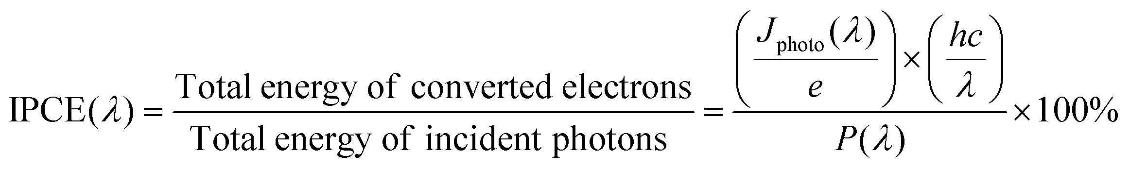
In the calculation of IPCE, optical losses such as reflection and transmission are disregarded, despite potentially having a large impact on the IPCE. In order to correct for these optical losses, the absorbed photon-to-current conversion efficiency (APCE) is often used to determine the quantum efficiency. The APCE is defined as the number of photogenerated charge carriers contributing to the photocurrent per absorbed photon, which is termed the internal quantum efficiency, and it can be expressed using the following equation:

3. PEC device configuration
Fig. 8 summarises the PEC device configurations reported so far (denoted type I–VI devices). Configuration (a), i.e. type I, is the simplest as it contains only one semiconducting light absorber, which we have referred to previously to illustrate the fundamental processes in PEC water splitting. A single semiconductor material can be used either as a photoanode or a photocathode to perform water oxidation or reduction. SrTiO3 (band-gap of 3.2 eV) and KTaO3 (3.5 eV) are widely used as photoanodes for PEC water splitting cells, with the aid of external bias. However, due to their large band-gap, only the UV portion of solar energy can be absorbed, and thus the theoretical maximum STH efficiency is limited to less than 1%. Later in this review, promising efficient photoelectrode materials will be further discussed. In most cases, in order to drive the separation of holes from electrons an external bias is needed for a single light absorber PEC system to function. | ||
| Fig. 8 Various PEC water splitting device configurations: (a) type I single light absorber; (b) type II heterojunction photoelectrode; (c) type III wired PEC tandem cell; (d) type IV wireless PEC tandem cell; (e) type V PV-PEC tandem cell; (f): type VI PV–electrolyser cell. | ||
Two or more semiconductors are often coupled for better utilisation of the solar spectrum and efficient charge carrier separation. Configuration (b), i.e. type II, is the heterojunction photoelectrode PEC device. In these systems, secondary semiconductors are loaded onto the primary absorber to improve light absorption and charge separation.8 Studies in this area have developed very rapidly within the last 10 years. A comprehensive recent review covering the state-of-the-art visible-driven heterojunction photoelectrodes has been conducted by us, and readers are directed to this for further examples.9 An additional PEC-based approach for water splitting is to utilise a series-connected photocathode and photoanode in a tandem configuration. The complete cell contains two light absorbers: a photoanode for water oxidation and a photocathode for water reduction. One conductive metal wire can be used for the wired configuration (configuration (c)) or a transparent conductive substrate can be used as an electron–hole recombination layer for the wireless configuration (configuration (d)). In both cases, the conduction band minimum of the photoanode must lie more negative than the valence band maximum of the photocathode to ensure complementary light absorption, whereby photons transmitted through the first material are then absorbed by the second. The main advantages of the PEC tandem cell are the increased photovoltage of the system and additional flexibility in material selection. A critical issue that needs to be addressed in the development of photocathodes and photoanodes in tandem stacks is the high photovoltage generated under illumination, but both sides must maintain a similar current density when no external bias is applied. Another device configuration based on unbiased water splitting is achieved by coupling a PV cell with a semiconductor photoelectrode represented by configuration (e), denoted as type V. In such a PV-PEC cell, the additional bias is applied to the photoelectrode by the PV material. The PV cell may be composed of single or multiple junctions, based on Si,10 group III–V materials,11 or hybrid perovskites.12 Wide band-gap semiconductors are preferred for the front photoelectrode, to enable adequate transmittance for further light harvesting by the PV. In addition, a transparent oxide layer is required between the PV and the PEC, providing a recombination layer for the photoinduced holes from the PV and electrons from the PEC (in the case of a PV–photoanode configuration). Turner et al. demonstrated such a monolithic tandem device based on a photocathode of p-type GaInP2 in combination with a GaAs p–n junction PV, recording a then benchmark STH efficiency of 12.4%. However, the short lifetime and high cost of the device limit its practical use.11 A device without a photoelectrode containing a shielded PV junction (known as a buried PV cell) is illustrated in configuration (f), denoted as type VI. Even though there is no semiconductor photoelectrode present, such a device can still be termed a PEC cell because light-driven electrochemical reactions occur within the cell. To date, the highest STH efficiency (30%) achieved by such a system consists of two polymer electrolyte membrane electrolysers in series with one InGaP/GaAs/GaInNAs(Sb) triple junction solar cell. However, this design still suffers from high materials cost, amongst other factors.2
4. Photoelectrode materials
4.1 Material requirements
The most important aspect for PEC water splitting, as mentioned in the Introduction, is the choice of a suitable photoanode and/or photocathode material. An ideal water splitting photoanode and/or photocathode requires semiconductor materials that possess the following characteristics:(i) Suitable band-gap energy and band positions. Natural sunlight consists of 5% UV (300–400 nm), 43% visible (400–700 nm), and 52% infrared radiation (700–2500 nm). Therefore, appreciable light absorption in the visible region is required to increase efficiency, and this in turn depends on the band-gap of the semiconductor. As the proton reduction potential is located at 0 V vs. NHE and the O2/H2O potential at 1.23 V vs. NHE (pH = 0), the theoretical minimum band-gap for water splitting requires incident photons with a minimum energy of 1.23 eV, which corresponds to a wavelength of light of ∼1100 nm. However, when considering the thermodynamic energy losses (0.3–0.4 eV) occurring during charge carrier transportation and the overpotential requirement for acceptable surface reaction kinetics (0.4–0.6 eV), a minimum band-gap of ∼1.8 eV is required, corresponding to light absorption at ca. 700 nm. The upper limit on the band-gap energy is 3.2 eV, because of the rapid drop in sunlight intensity below 390 nm according to the solar spectrum.
Therefore, for a single semiconductor photoelectrode, a band-gap energy between 1.9 eV and 3.2 eV is desirable to obtain sizable photovoltages. Theoretically, a band-gap of ca. 2.0 eV is preferred for optimal sunlight utilization, in addition to the thermodynamic band position requirements.13 However, in practice, it has hardly been achieved because the expected photovoltage can seldom be met. Without high photovoltages (>1.61 V), even the highest current density will not solve the problem of unbiased water splitting and thus external bias or tandem devices are needed to provide the extra voltage to split water. Fig. 9 illustrates the band-gaps and band positions of typical n-type and p-type semiconductors utilised for PEC water splitting at pH = 0. It is noteworthy that the band positions of oxide semiconductors vary depending on the pH of the electrolyte, since VH (as illustrated in Fig. 6) depends on the pH of the solution (by −0.059 V per pH unit) with respect to the redox potential of the electrolyte. Furthermore, according to the Nernst equation, the water reduction and oxidation potentials change in a similar manner to the band positions (i.e. −0.059 V per unit pH). It is generally accepted that the Nernstian dependence indicates that H+ and OH− are potential-determining ions (PDI) adsorbed on the semiconductor surface within the Helmholtz layer. For other materials, such as metal sulfides, the PDIs can be different and therefore the pH dependence is more complicated14 (a diagram showing this can be found in the ESI,† Fig. S1).
 | ||
| Fig. 9 Band positions of various semiconductors with respect to the redox potentials of water splitting at pH = 0. | ||
Overall, the band positions of most semiconductors, in particular oxides, show the same pH dependence as represented by the Nernst equation, whereas the band positions are fixed with respect to the water redox potentials. Hence, the relative difference between the band positions of an oxide photocatalyst and the water redox potential is pH independent.
(ii) Efficient charge carrier separation and transportation in the semiconductor. Fast charge recombination is a major factor contributing to low STH efficiencies, and thus a strategy to promote efficient charge carrier separation and transport is required, which depends both on the intrinsic properties (hole and electron mobility) and on the extrinsic properties (crystallinity, nanostructure) of the material.
(iii) Strong catalytic activity and stability. Suitably rapid surface reaction kinetics can avoid surface charge accumulation, which would otherwise lead to electron–hole recombination. Photocorrosion is a major problem for many candidate water splitting semiconductors, in particular metal sulfides, and occurs when the photogenerated holes/electrons do not oxidise/reduce water but instead decompose the photocatalyst itself. These photocorrosion reactions depend upon the relative positions of the semiconductor band edges and the respective decomposition potentials. Anodic photocorrosion can occur if the anodic decomposition potential (Epd) is above the valence band potential of the semiconductor. Conversely, cathodic photocorrosion can occur if the cathodic decomposition potential (End) is below the conduction band of the semiconductor. Metal oxides, such as BiVO4 and ZnO, or metal sulphides, such as MoS2 and CdS, can easily undergo anodic photocorrosion depending on the pH of the electrolyte, since the actual values of the decomposition potentials depend upon the pH value. However, common photoanode materials such as TiO2 and Fe2O3, even though their anodic deposition potential is above the valance band potential, are thermodynamically stable because of their very slow decomposition reaction kinetics.
In addition, the photoelectrode materials should be low-cost and composed of earth-abundant elements for practical applications. This is crucial toward justifying the argument for an economical scale-up of solar-to-fuel devices.
4.2 Photoanode materials
Numerous photoanode materials for PEC water splitting have been reported over the past 10–20 years, reflecting the great amount of research invested in this area. This section summarises the most promising low-cost and efficient photoanodes employed so far, and puts forward potential strategies to improve their performance.Nevertheless, the recently reported benchmark photocurrent and STH efficiency for haematite (4.68 mA cm−2 at 1.23 V vs. RHE, STH of ca. 0.55%) achieved by a vertically-grown haematite nanosheet film modified with Ag nanoparticles and Co–Pi co-catalyst suggests that much more work is required to improve its STH performance, given that the limitations of the material are fairly well understood.22
The poor surface reaction kinetics can be improved by the addition of oxygen evolution co-catalysts such as Co–Pi (cobalt phosphate). For example, a Co–Pi modified junction nanoparticulate BiVO4/ZnO nanorod exhibited a photocurrent of ca. 3 mA cm−2 at 1.23 V vs. RHE; the function of the vertical ZnO nanowires was to trap light and improve electron transfer to the counter electrode.26 Recently, a benchmark photocurrent of 2.73 mA cm−2 at a potential as low as 0.6 V vs. RHE and an ABPE of 1.7% was achieved on a nanoporous BVO photoanode with a dual-layer FeOOH/NiOOH co-catalyst.27 Furthermore, by assembling a PV-PEC tandem system composed of a silicon solar cell and a BVO photoanode, an STH efficiency of 4.6% was achieved.10 Beyond this, a nanocone Mo:BiVO4/Fe(Ni)OOH photoanode exhibited a record photocurrent of 5.82 mA cm−2 at 1.23 V vs. RHE. Together with a single perovskite solar cell, the tandem device exhibited unassisted water splitting with an STH conversion efficiency of 6.2%.28
4.3 Photocathode materials
As shown in Fig. 9, the conduction band positions of p-type semiconductors such as cuprous oxide (Cu2O) and Si are more negative than the redox potential of H+/H2, and thus they can be employed as photocathodes for proton reduction. However, in most cases their application is still limited, due to their facile cathodic photocorrosion in solution.35,36(a) GaP. GaP has an indirect band-gap of 2.26 eV, with a conduction band edge located at −0.6 V vs. NHE at pH = 0 and thus could be used for photocatalytic water reduction to produce H2. Due to its large photovoltage, unbiased overall water splitting can be achieved through coupling with another photoanode material. Although the n-type GaP is unstable in aqueous solution, p-type GaP is stable for extended periods of time under water reduction conditions. The overall STH efficiency of GaP is limited by its small minority carrier diffusion length. There are relatively few reports of GaP for PEC water splitting, apart from one-dimensional GaP nanowires decorated with platinum co-catalysts. Therefore, readers are directed to the ESI† for further reading.
(b) InP-based photoanode. InP exhibits a band-gap of 1.35 eV, representing near-optimal absorptivity of the solar spectrum. However, the very high cost of InP limits its commercial processibility as a photoelectrode for water splitting. Notten et al. fabricated a photocathode composed of InP nanowire arrays with molybdenum sulfide electrocatalysts for H2 production, with an overall STH of 6.4% under one-sun irradiation. However, the authors claimed that the performance of InP-based photoelectrodes was limited by severe photocorrosion.38 Therefore, amorphous TiO2 has been employed as a surface passivation layer to isolate the InP photoelectrode from the electrolyte. One should also note that the large valence band offset between TiO2 and these metal phosphides can create an energy barrier for holes reaching the surface, reducing recombination at the surface. Readers are directed towards the ESI† for additional reading regarding group II–IV metal phosphide photoelectrodes.
It is worth mentioning that Hannappel and co-workers have developed an efficient tandem cell based on group III–V materials. The tandem structure consists of a GaInP n–p top cell (Eg = 1.78 eV) and GaInAs n–i–p bottom cell (Eg = 1.26 eV) with Rh electrocatalysts deposited onto the surface. The as-prepared tandem device yields an STH of 14% and 17% for unbiased and potentiostatically assisted water splitting, respectively, which is the present benchmark efficiency for a tandem PEC device.39
4.4 Co-catalyst selection
Electrolysis requires the application of a potential greater than 1.23 VRHE between anode and cathode because of kinetic barriers that are commonly encountered in performing multielectron reactions. For example, oxygen evolution from water requires four electrons and generates four intermediate species.41 On most bare semiconductor surfaces, the formation of intermediate species presents a large energy barrier to oxygen/hydrogen evolution and thus an overpotential is necessary to drive the kinetically rate-limiting multistep oxidation/reduction reactions. In the case of photoelectrodes, the electrocatalytic behaviour occurs at the semiconductor–liquid surface and surface co-catalysts are often loaded to reduce the overpotential (activation energy) and suppress surface recombination by acting as electron–hole acceptors.Typically, these co-catalysts are deposited on the electrode as thin layers or islands (nanoparticles) to minimize their light absorption or scattering. For a well-performing co-catalyst, both a strong overpotential for OER/HER and appreciable stability under the operating conditions are important. Fig. 10 shows the qualitative effect of a surface oxygen evolution co-catalyst on photoanode performance. In order to drive a current density of 10 mA cm−2, a 0.6 V overpotential is needed for a poor-performing co-catalyst, whereas only 0.3 V of overpotential is needed for a “good” co-catalyst. Since the choice of oxygen evolution catalysts has no effect on the thermodynamics of the reaction, the open-circuit voltage (VOC) should be the same for any co-catalyst. However the overall water splitting efficiency is largely limited by the co-catalyst selection.42
 | ||
| Fig. 10 Schematic diagram showing the qualitative effect of a surface co-catalyst on photoanode water oxidation performance; the dotted curve represents the dark current with a good or bad co-catalyst; the solid curve represents the photocurrent of a photoanode when coupling a good or bad co-catalyst. Reproduced from ref. 42 with permission of the American Chemical Society. | ||
Noble metal-based catalysts such as IrO2 and RuO2 are among the highest performing water oxidation evolution catalysts, but are prohibitively expensive due to their low earth-abundance and therefore in recent years a great deal of effort has concentrated on developing low-cost first-row transition metal oxide OER catalysts. Jaramillo and co-workers have benchmarked various heterogeneous metal oxide OER electrocatalysts, based on the overpotential required to achieve a current density of 10 mA cm−2.43,44 Among all metal oxide based OECs, cobalt oxide (prepared by electrodeposition) has emerged as a robust, efficient water oxidation co-catalyst and can operate under neutral conditions. Nocera and co-workers prepared cobalt oxide films from cobalt salts in phosphate buffer (Co–Pi) or borate buffer (Co–Bi) solutions at potentials above 1.1 V vs. NHE.45 The obtained co-catalyst was amorphous and contained substantial amounts of phosphate or borate anions. The buffer solution was essential for the deposition of highly active films and to maintain their stability. However, the films were unstable in the electrolyte in the absence of applied bias. The growth mechanism of Co–Pi films for water oxidation has been investigated by electron paramagnetic resonance (EPR) spectroscopy. During the in situ electrodeposition, changes in the EPR signals were found to correspond to the change in the populations of Co(II) and Co(IV). As the deposition voltage increased into the water oxidation region, the population of Co(II) decreased while that of Co(IV) increased, which is evidence for the formation of Co(IV) species during water oxidation at neutral pH.46 Other co-catalysts, such as nickel oxide (NiOx), have been extensively studied in the literature and have been prepared by various methods. NiOx films generally convert to either Ni(OH)2 or NiOOH during the water oxidation reaction in alkaline electrolytes (e.g. KOH solution). Yan and co-workers found that highly nanostructured α-Ni(OH)2 nanocrystals were a remarkably active and stable OER catalyst in alkaline media, displaying a current density of 10 mA cm−2 at a small overpotential of 0.331 V and exhibiting a small Tafel slope of 42 mV per decade.47 Ni–Bi film prepared with precise thickness control and operating at a modest overpotential provided an alternative to the Co–OEC catalyst. It was also found that Ni–Bi could undergo self-healing in the proper electrolyte (potassium borate solution), enabling long periods of water oxidation.48
These earth-abundant electrocatalysts are also useful to passivate unstable semiconductors such as ZnO and silicon, and thus exhibit additional functionality.49 Dai and co-workers demonstrated that a thin layer of Ni metal prepared by thermal evaporation exhibits bi-functionality as both OEC and passivation layer for silicon photoanodes.50 In addition, Naldoni et al. demonstrated that a thin layer of photodeposited amorphous NiOOH coupled onto haematite photoanodes could reduce the overpotential by 150 mV and increase the photocurrent by about 50% at 1.23 V vs. RHE.51 Furthermore, Mullins and co-workers deposited α-FeOOH onto a Si triple junction solar cell; the obtained photoanode (α-FeOOH/Si) achieved an STH efficiency of 4.3% at 0 V vs. RHE in a three-electrode configuration with a 4 h lifetime.52 It is well known that the incorporation of iron species into a nickel hydroxide electrocatalyst forms a NiFe double hydroxide (NiFe-LDH). These Ni–Fe LDH electrocatalysts can be prepared by hydrothermal or photoelectrodeposition directly onto light-absorbing photoelectrodes, such as Ta3N5, which can dramatically improve the photocurrent and stability. Recently, Domen demonstrated that nanoworm-like BiVO4 with Ni–Fe-LDH modification can exhibit a high STH efficiency (2.25%) and long-term durability (10 h) in 1 M potassium borate electrolyte (pH = 9.3) under AM 1.5G one sun illumination.53 More recently, Grätzel et al. reported that a hydrothermally-grown Ni–Fe LDH catalyst could be combined with a 17%-efficient CH3NH3PbI3 perovskite solar cell to split water with an STH of 12.3%.12 Very recently, Luo et al. demonstrated that low-cost α-FeOOH film could be fabricated by a facile chemical bath deposition followed by a rapid heat treatment, which will guide the further development of new low-cost electrocatalysts for oxygen production via water splitting.54
On the other hand, for water reduction, noble metals such as platinum (Pt) are frequently used due to their low overpotential and strong corrosion resistance. However, non-precious hydrogen evolution catalysts, including metal disulfides, selenides, carbides, nitrides, phosphides, and heteroatom-doped nanocarbons, are essential for economical H2 production, the majority of which have been summarised in the recent review by Zhang et al.,55 and therefore research should be directed to using these to reduce the overall cost of a PEC device.
Table S1 in the ESI† summarises the performance of promising efficient PEC devices that use a combination of efficient photoelectrodes and co-catalysts. PV-based PEC devices (PV-PEC and buried PV) have achieved STH efficiencies >10%. However, their high cost and low stability are still major limiting factors that prevent their commercialisation. Research in this area continues in order to design and produce a cost-effective, highly efficient and stable photoanode and/or photocathode for oxygen and/or hydrogen production. Several strategies so far have been adopted to enhance the performance of PEC devices, including: (1) combinations of different materials, (2) materials nanoarchitecture design, (3) co-catalyst modification and (4) deposition of surface protection layers, which have all been detailed above.
5. Conclusions and outlook
This review presents the fundamental aspects of PEC water splitting and different device assemblies. Readers are directed towards the ESI† for additional comprehensive monographs on the detailed working principles and scientific challenges of solar-driven water splitting. In essence, to achieve unassisted water splitting using a single semiconductor, the band-gap must straddle the reduction and oxidation potentials of water so that photoexcited electrons and holes have sufficient overpotential for the hydrogen and oxygen evolution reactions, respectively. Wide band-gap semiconductors such as TiO2 are inexpensive and stable, but not effective for sunlight harvesting. Even though α-Fe2O3 and BiVO4 exhibit a broader absorption than TiO2, the achieved photocurrents for these materials fall short of their theoretical maxima, due to the fast charge carrier recombination and poor surface OER kinetics. Narrow band-gap semiconductors, such as CdS, Si, and group III–V compounds, have the potential to achieve high efficiency but suffer from instability over long periods. The ultimate target of the entire solar fuel research field is to design and produce a cost-effective, highly efficient and stable photoanode and/or photocathode for oxygen and/or hydrogen production, either by employing a particulate system or a PEC device. The past decade has witnessed many innovations in combinations of materials, nanoarchitecture design and co-catalyst optimisation which address the main issues existing in the reported efficient photoelectrodes. Furthermore, the addition of thin surface protection layers by evolving techniques such as ALD has benefitted the field in enhancing the stability and long-term performance of a PEC device. One concern may be the reproducibility in reporting device efficiencies – some degree of standardisation is necessary as the substantial differences in experimental setups and conditions (e.g. light sources with/without certification) have led to discrepancies in PEC efficiencies between groups. In terms of PEC configurations, type V (PEC-PV) and VI (PV–electrolyser tandem) devices are a viable option toward achieving highly efficient unassisted solar water splitting in the near future. However, as these systems require more than two PV cells in tandem, they are unlikely to be economically viable unless the cost of materials substantially decreases. To some extent, research in this field is driven by political and economic factors: for example the priorities of local governments toward sustainable energy and climate change as well as the current oil price. In the longer term, a simple but efficient PEC (either type II, III or IV) device should be developed, due to the low cost in both materials and maintenance. Currently governmental attitudes toward renewables also greatly influence the direction of research between CO2 photoreduction and PEC water splitting for H2 fuel. There is no doubt that this research is crucial to establishing a sustainable society based on abundant solar energy. Another challenge is how to encourage engineers and materials scientists to work together to address the capture, separation, storage and purity issues of the produced solar fuels. In the personal opinions of the authors, a low-cost PEC tandem cell (again type II and IV devices) that utilises earth-abundant semiconductors and first-row transition metal co-catalysts has the greatest potential to achieve a sustainable future for our renewable energy supplies.Acknowledgements
C. J. acknowledges funding from the China Scholarship Council (CSC File No. 201308060090) and S. M. and J. T. gratefully acknowledge funding from EPSRC Grant No. EP/N009533/1.References
- J. Barber, Chem. Soc. Rev., 2009, 38, 185–196 RSC.
- J. Y. Jia, L. C. Seitz, J. D. Benck, Y. J. Huo, Y. S. Chen, J. W. D. Ng, T. Bilir, J. S. Harris and T. F. Jaramillo, Nat. Commun., 2016, 7, 13237 CrossRef CAS PubMed.
- R. Van de Krol and M. Grätzel, Photoelectrochemical hydrogen production, Springer, Switzerland, 2012 Search PubMed.
- D. M. Smyth, The Defect Chemistry of Metal Oxides, Oxford University Press, Oxford, 2000 Search PubMed.
- X. Zhang, H. Li, S. Wang, F.-R. F. Fan and A. J. Bard, J. Phys. Chem. C, 2014, 118, 16842–16850 CAS.
- S. Licht, A. J. Bard and M. Stratmann, Semionductor eletrodes and Photoelectrochemistry, Wiley-VCH, Weinheim, 2002 Search PubMed.
- Z. Zhang and J. T. Yates, Chem. Rev., 2012, 112, 5520–5551 CrossRef CAS PubMed.
- X. An, T. Li, B. Wen, J. Tang, Z. Hu, L. M. Liu, J. Qu, C. Huang and H. Liu, Adv. Energy Mater., 2016, 6, 1502268 CrossRef.
- S. J. A. Moniz, S. A. Shevlin and D. J. Martin, Energy Environ. Sci., 2015, 8, 731–759 CAS.
- F. F. Abdi, L. Han, A. H. Smets, M. Zeman, B. Dam and R. van de Krol, Nat. Commun., 2013, 4, 2195 Search PubMed.
- O. Khaselev, Science, 1998, 280, 425–427 CrossRef CAS PubMed.
- J. Luo, J.-H. Im, M. T. Mayer, M. Schreier, M. K. Nazeeruddin, N.-G. Park, S. D. Tilley, H. J. Fan and M. Grätzel, Science, 2014, 345, 1593–1596 CrossRef CAS PubMed.
- A. Murphy, P. Barnes, L. Randeniya, I. Plumb, I. Grey, M. Horne and J. Glasscock, Int. J. Hydrogen Energy, 2006, 31, 1999–2017 CrossRef CAS.
- Y. Xu and M. A. Schoonen, Am. Mineral., 2000, 85, 543–556 CrossRef CAS.
- H. Xu, S. Ouyang, L. Liu, P. Reunchan, N. Umezawa and J. Ye, J. Mater. Chem. A, 2014, 2, 12642–12661 CAS.
- S. Piskunov, O. Lisovski, J. Begens, D. Bocharov, Y. F. Zhukovskii, M. Wessel and E. Spohr, J. Phys. Chem. C, 2015, 119, 18686–18696 CAS.
- X. Chen, L. Liu, P. Y. Yu and S. S. Mao, Science, 2011, 331, 746–750 CrossRef CAS PubMed.
- K. Sivula, F. L. Formal and M. Gratzel, ChemSusChem, 2011, 4, 432–449 CrossRef CAS PubMed.
- D. A. Wheeler, G. Wang, Y. Ling, Y. Li and J. Z. Zhang, Energy Environ. Sci., 2012, 5, 6682–6702 CAS.
- Q. Yu, X. Meng, T. Wang, P. Li and J. Ye, Adv. Funct. Mater., 2015, 25, 2686–2692 CrossRef CAS.
- L. Steier, I. Herraiz-Cardona, S. Gimenez, F. Fabregat-Santiago, J. Bisquert, S. D. Tilley and M. Grätzel, Adv. Funct. Mater., 2014, 24, 7681–7688 CrossRef CAS.
- P. Peerakiatkhajohn, J.-H. Yun, H. Chen, M. Lyu, T. Butburee and L. Wang, Adv. Mater., 2016, 28, 6405–6410 CrossRef CAS PubMed.
- A. Kudo, K. Ueda, H. Kato and I. Mikami, Catal. Lett., 1998, 53, 229–230 CrossRef CAS.
- Y. Park, K. J. McDonald and K.-S. Choi, Chem. Soc. Rev., 2013, 42, 2321–2337 RSC.
- S. K. Pilli, T. E. Furtak, L. D. Brown, T. G. Deutsch, J. A. Turner and A. M. Herring, Energy Environ. Sci., 2011, 4, 5028–5034 CAS.
- S. J. A. Moniz, J. Zhu and J. Tang, Adv. Energy Mater., 2014, 4, 1301590 CrossRef.
- T. W. Kim and K.-S. Choi, Science, 2014, 343, 990–994 CrossRef CAS PubMed.
- Y. Qiu, W. Liu, W. Chen, G. Zhou, P.-C. Hsu, R. Zhang, Z. Liang, S. Fan, Y. Zhang and Y. Cui, Sci. Adv., 2016, 2, e1501764 Search PubMed.
- R. Liu, Z. Zheng, J. Spurgeon and X. Yang, Energy Environ. Sci., 2014, 7, 2504–2517 CAS.
- M. F. Lichterman, A. I. Carim, M. T. McDowell, S. Hu, H. B. Gray, B. S. Brunschwig and N. S. Lewis, Energy Environ. Sci., 2014, 7, 3334–3337 CAS.
- A. Pareek, P. Paik and P. H. Borse, Langmuir, 2014, 30, 15540–15549 CrossRef CAS PubMed.
- G. Ai, H. Li, S. Liu, R. Mo and J. Zhong, Adv. Funct. Mater., 2015, 25, 5706–5713 CrossRef CAS.
- S. Hu, M. R. Shaner, J. A. Beardslee, M. Lichterman, B. S. Brunschwig and N. S. Lewis, Science, 2014, 344, 2547–2552 CrossRef PubMed.
- K. Sun, F. H. Saadi, M. F. Lichterman, W. G. Hale, H.-P. Wang, X. Zhou, N. T. Plymale, S. T. Omelchenko, J.-H. He and K. M. Papadantonakis, Proc. Natl. Acad. Sci. U. S. A., 2015, 112, 3612–3617 CAS.
- A. Paracchino, N. Mathews, T. Hisatomi, M. Stefik, S. D. Tilley and M. Grätzel, Energy Environ. Sci., 2012, 5, 8673 CAS.
- K. Sun, S. Shen, Y. Liang, P. E. Burrows, S. S. Mao and D. Wang, Chem. Rev., 2014, 17, 8662–8719 CrossRef PubMed.
- A. Paracchino, V. Laporte, K. Sivula, M. Grätzel and E. Thimsen, Nat. Mater., 2011, 10, 456–461 CrossRef CAS PubMed.
- L. Gao, Y. Cui, J. L. Wang, A. Cavalli, A. Standing, T. T. T. Vu, M. A. Verheijen, J. E. M. Haverkort, E. P. A. M. Bakkers and P. H. L. Notten, Nano Lett., 2014, 14, 3715–3719 CrossRef CAS PubMed.
- M. M. May, H.-J. Lewerenz, D. Lackner, F. Dimroth and T. Hannappel, Nat. Commun., 2015, 6, 8286 CrossRef CAS PubMed.
- L. Ji, M. D. Mcdaniel, S. Wang, A. B. Posadas, X. Li, H. Huang, J. C. Lee, A. A. Demkov, A. J. Bard and J. G. Ekerdt, Nat. Nanotechnol., 2015, 10, 84–90 CrossRef CAS PubMed.
- M. T. Koper, J. Electroanal. Chem., 2011, 660, 254–260 CrossRef CAS.
- M. G. Walter, E. L. Warren, J. R. McKone, S. W. Boettcher, Q. Mi, E. A. Santori and N. S. Lewis, Chem. Rev., 2010, 110, 6446–6473 CrossRef CAS PubMed.
- C. C. L. McCrory, S. Jung, J. C. Peters and T. F. Jaramillo, J. Am. Chem. Soc., 2013, 135, 16977–16987 CrossRef CAS PubMed.
- C. C. L. McCrory, S. Jung, I. M. Ferrer, S. M. Chatman, J. C. Peters and T. F. Jaramillo, J. Am. Chem. Soc., 2015, 137, 4347–4357 CrossRef CAS PubMed.
- M. W. Kanan and D. G. Nocera, Science, 2008, 321, 1072–1075 CrossRef CAS PubMed.
- J. G. McAlpin, Y. Surendranath, M. Dincă, T. A. Stich, S. A. Stoian, W. H. Casey, D. G. Nocera and R. D. Britt, J. Am. Chem. Soc., 2010, 132, 6882–6883 CrossRef CAS PubMed.
- M. Gao, W. Sheng, Z. Zhuang, Q. Fang, S. Gu, J. Jiang and Y. Yan, J. Am. Chem. Soc., 2014, 136, 7077–7084 CrossRef CAS PubMed.
- M. Dincă, Y. Surendranath and D. G. Nocera, Proc. Natl. Acad. Sci. U. S. A., 2010, 107, 10337–10341 CrossRef PubMed.
- C. Jiang, S. J. A. Moniz, M. Khraisheh and J. Tang, Chem. – Eur. J., 2014, 20, 12954–12961 CrossRef CAS PubMed.
- M. J. Kenney, M. Gong, Y. Li, J. Z. Wu, J. Feng, M. Lanza and H. Dai, Science, 2013, 342, 836–840 CrossRef CAS PubMed.
- F. Malara, A. Minguzzi, M. Marelli, S. Morandi, R. Psaro, V. Dal Santo and A. Naldoni, ACS Catal., 2015, 5, 5292–5300 CrossRef CAS.
- W. D. Chemelewski, H. Lee, J. Lin, A. J. Bard and C. B. Mullins, J. Am. Chem. Soc., 2014, 136, 2843–2850 CrossRef CAS PubMed.
- Y. Kuang, Q. Jia, H. Nishiyama, T. Yamada, A. Kudo and K. Domen, Adv. Energy Mater., 2016, 6, 1501645 CrossRef.
- W. Luo, C. Jiang, Y. Li, S. A. Shevlin, X. Han, K. Qiu, Y. Cheng, Z. Guo, W. Huang and J. Tang, J. Mater. Chem. A, 2017, 5, 2021–2028 CAS.
- X. Zou and Y. Zhang, Chem. Soc. Rev., 2015, 25, 2609–2615 Search PubMed.
Footnote |
| † Electronic supplementary information (ESI) available. See DOI: 10.1039/c6cs00306k |
| This journal is © The Royal Society of Chemistry 2017 |