
 Open Access Article
 This Open Access Article is licensed under a
 Creative Commons Attribution 3.0 Unported Licence
Colloidal metal oxide nanocrystals as charge transporting layers for solution-processed light-emitting diodes and solar cells
Xiaoyong
Liang†
a,
Sai
Bai†
b,
Xin
Wang
a,
Xingliang
Dai
a,
Feng
Gao
b,
Baoquan
Sun
c,
Zhijun
Ning
d,
Zhizhen
Ye
*a and
Yizheng
Jin
 *e
*e
aState Key Laboratory of Silicon Materials, School of Materials Science and Engineering, Zhejiang University, Hangzhou 310027, People's Republic of China. E-mail: yezz@zju.edu.cn
bDepartment of Physics, Chemistry and Biology (IFM), Linköping University, SE-581 83 Linköping, Sweden
cJiangsu Key Laboratory for Carbon-Based Functional Materials & Devices, Institute of Functional Nano & Soft Materials (FUNSOM), Soochow University, Suzhou 215123, People's Republic of China
dShanghai Tech University, China
eCenter for Chemistry of High-Performance & Novel Materials, State Key Laboratory of Silicon Materials, Department of Chemistry, Zhejiang University, Hangzhou 310027, People's Republic of China. E-mail: yizhengjin@zju.edu.cn
First published on 28th February 2017
Abstract
Colloidal metal oxide nanocrystals offer a unique combination of excellent low-temperature solution processability, rich and tuneable optoelectronic properties and intrinsic stability, which makes them an ideal class of materials as charge transporting layers in solution-processed light-emitting diodes and solar cells. Developing new material chemistry and custom-tailoring processing and properties of charge transporting layers based on oxide nanocrystals hold the key to boosting the efficiency and lifetime of all-solution-processed light-emitting diodes and solar cells, and thereby realizing an unprecedented generation of high-performance, low-cost, large-area and flexible optoelectronic devices. This review aims to bridge two research fields, chemistry of colloidal oxide nanocrystals and interfacial engineering of optoelectronic devices, focusing on the relationship between chemistry of colloidal oxide nanocrystals, processing and properties of charge transporting layers and device performance. Synthetic chemistry of colloidal oxide nanocrystals, ligand chemistry that may be applied to colloidal oxide nanocrystals and chemistry associated with post-deposition treatments are discussed to highlight the ability of optimizing processing and optoelectronic properties of charge transporting layers. Selected examples of solution-processed solar cells and light-emitting diodes with oxide-nanocrystal charge transporting layers are examined. The emphasis is placed on the correlation between the properties of oxide-nanocrystal charge transporting layers and device performance. Finally, three major challenges that need to be addressed in the future are outlined. We anticipate that this review will spur new material design and simulate new chemistry for colloidal oxide nanocrystals, leading to charge transporting layers and solution-processed optoelectronic devices beyond the state-of-the-art.
 Xiaoyong Liang | Xiaoyong Liang is currently a PhD candidate under the supervision of Professor Yizheng Jin in the State Key Laboratory of Silicon Materials, School of Materials Science and Engineering at Zhejiang University. He has keen interest in interfacial engineering of solution-processed optoelectronics using metal oxides as charge-transport layers. Now he is working on quantum dot LEDs. |
 Sai Bai | Sai Bai obtained his PhD degree in Materials Physics and Chemistry from Zhejiang University in 2014, focusing on solution processable metal oxide films for optoelectronic applications. He is current a VINNMER Fellow and Marie Curie Fellow in Linköping University, Sweden and University of Oxford, UK. His research interests include metal oxide nanocrystals, organic photovoltaics, perovskite solar cells and perovskite light-emitting diodes. |
 Yizheng Jin | Dr Yizheng Jin is a Professor of Chemistry at Zhejiang University, China. His research interests encompass material chemistry, device engineering and device physics of solution-processed optoelectronics. His research has resulted in over 50 papers in peer-reviewed journals, including Nature, Nat. Photonics, J. Am. Chem. Soc. and Adv. Mater. Prof. Jin has received several awards, including National Natural Science Funds for Excellent Young Scholar, Chinese Chemical Society Award for Outstanding Young Chemist, Qiu-Shi Young Scholars Award and Top 10 scientific advances of 2014 in China. |
1. Introduction
The exciting discoveries and tremendous progress of material chemistry create families of solution-processed semiconductors, including conjugated polymers,1,2 colloidal quantum dots (QDs)3–5 and organic–inorganic hybrid lead–halide hybrid perovskites.6,7 These materials with intriguing optoelectronic properties can be processed as thin films by high-throughput and vacuum-free printing and coating techniques, such as inkjet-printing, roll-to-roll printing and blade-coating.8–16 Many printing and coating procedures can be completed at low temperatures. Therefore, they are compatible with flexible and light-weight plastic substrates. These merits promise an unprecedented generation of low-cost, large-area and flexible light-emitting diodes (LEDs) and solar cells processed by solution-based techniques.High-performance LEDs and solar cells are no doubt the results of extraordinary cooperation of multiple functional components. For the state-of-the-art solution-processed LEDs or solar cells, charge transporting layers (CTLs), i.e. electron transporting layers (ETLs) and hole transporting layers (HTLs), are essential components (Fig. 1). CTLs affect not only charge injection (or extraction) into (or out of) the active layers, but also many other elementary physical processes for device operation, such as interfacial charge recombination and light extraction (or light absorption) in LEDs (or solar cells). The integration of CTLs with desirable properties is critical in terms of improving device performance.
 | ||
| Fig. 1 Typical device structures of solution-processed (A) LEDs and (B) solar cells. | ||
For large-scale production of solution-processed optoelectronics, ideally, not only the active layers but also all the other components should be able to be deposited by solution-based techniques. In this regard, various solution-processed materials have been explored as CTLs. Among them, colloidal metal oxide nanocrystals have attracted great interest.17–24 The best example is ETLs based on colloidal ZnO nanocrystals, which have been employed in several best-performing proto-type devices, including the quantum-dot LEDs (QLEDs) developed by our group,18 the quantum-dot solar cells (QDSCs) developed by the Sargent group22 and the perovskite LEDs developed by the Wang and Huang group.23 Many other reports showed that colloidal oxide nanocrystals with high work function, e.g. NiO nanocrystals,24,25 can be used to fabricate high-quality HTLs for LEDs and solar cells. Furthermore, colloidal oxide nanocrystals are fully compatible with large-scale industrial production. For example, Krebs and co-workers prepared polymer solar cell modules in which ZnO nanocrystals were deposited as ETLs by a modified slot-die coating procedure.26,27 These facts highlight a promising future of integrating colloidal oxide nanocrystals as CTLs in solution-processed LEDs and solar cells to achieve high-performance, low-cost and large-area devices.
This review article aims to provide illustrative accounts on the current status of CTLs based on oxide nanocrystals. The progress of utilizing colloidal oxide nanocrystals as CTLs for solution-processed LEDs and solar cells is based on the developments of two important research fields, synthetic chemistry of colloidal oxide nanocrystals and interfacial engineering of optoelectronic devices. There are already good review articles dedicated to either the synthetic chemistry of colloidal oxide nanocrystals28–32 or interfacial engineering of solution-processed optoelectronics.33–43 Nevertheless, on the basis of our practices in the past several years, we believe that there is a gap between the community of chemists synthesizing oxide nanocrystals and the community of researchers working on solution-processed optoelectronics. We would like to provide an in-depth review which correlates chemistry of colloidal oxide nanocrystals, processing and optoelectronic properties of CTLs, and device performance of solution-processed solar cells and LEDs. A personal selection of examples is presented to systematize the knowledge bridging the two fields, chemistry of colloidal oxide nanocrystals and interfacial engineering of solution-processed LEDs and solar cells.
We will begin with a summary of the general requirements that should be fulfilled by CTLs and point out the unique advantages of colloidal oxide nanocrystals as CTLs. Next, a brief overview of chemistry of colloidal oxide nanocrystals will be presented. Synthetic chemistry of colloidal oxide nanocrystals, ligand chemistry that may be applicable to colloidal oxide nanocrystals and chemistry associated with post-deposition treatments will be covered. The applications of colloidal oxide nanocrystals as CTLs in solar cells and LEDs will be summarized in the subsequent two chapters. Emphasis will be placed on the correlation between the properties of oxide-nanocrystal CTLs and device performance. The last chapter of this review will list three major directions that we believe are critical for future development of oxide-nanocrystal CTLs.
2. General requirements for solution-processed CTLs
An essential requirement for solution-processed CTLs used in optoelectronics is that they should be able to be integrated into devices by solution-based methods. Formulation of inks with sufficiently high concentration and good stability is indispensable to fabricate continuous and pinhole-free CTL films with controllable thickness. For all-solution processed devices, multiple layers, including the ETLs and HTLs, shall be processed from solutions. This often involves the use of orthogonal solvent systems for the deposition of different materials to avoid dissolution of underlying layers. Moreover, processing of top CTLs should exclude high-temperature annealing which may damage the active layers or other components in the devices. Low processing temperatures, i.e. <150 °C, are highly desirable so that the processing procedures are compatible with flexible substrates.CTLs should be of good stability. First and foremost, CTLs themselves must be sufficiently stable within the lifetime of devices. Second, all interfaces involving CTLs, e.g. the interfaces of active layer/ETL, active layer/HTL, cathode/ETL and anode/HTL, should be stable and the contact properties should not deteriorate under long-time operational conditions. Third, in device operation, the active layers are in the excited states, which are generally sensitive to oxygen or moisture. The environmental stability of devices can be greatly improved if CTLs act as barriers for oxygen and moisture diffusion.
The chemistry of CTLs should be versatile and robust to allow systematic and purposeful engineering of their optoelectronic properties. Here we use QLEDs and bulk-heterojunction (BHJ) organic solar cells as examples to show that the optoelectronic properties of CTLs, i.e. work function, band structure, conductivity, intragap states, optical properties, etc., impact almost all the elementary processes of device operation.
As shown in Fig. 2, elementary processes for QLED operation involve (1) charge injection from electrodes into CTLs, (2) charge transport in the CTLs, (3) charge injection from the CTLs into QD layers, (4) formation of excitons in the QDs, (5) radiative decay of the excitons to generate photons, and (6) photon emission out of the devices. The energy-level alignment at the interfaces of electrode/CTLs and QD/CTLs determines the charge injection efficiency. Efficient charge injection into the QDs relies on high conductivity of CTLs and negligible energy barriers at the interfaces to minimize potential-drops. Efficient exciton formation demands both balanced charge injection and effective charge confinement within the QD layer. Charge selective CTLs with good blocking properties are beneficial to realize effective charge confinement. Balanced charge injection requires modulation of both electron injection and hole injection so that injection rates of the two types of carriers can match each other. In general, the ionization potential of many QD emitters is much higher than that of most organic semiconductors. Thus, conventional organic HTLs developed for organic emitters cannot achieve efficient hole injection in QLEDs. Excess injection of one type of charge causes many problems, such as a decrease of the fraction of injected charges that form excitons, charging of QDs which generates less efficient trion emission,44,45 and deterioration of device lifetime.18 Interactions between CTLs and excitons formed in QDs often cannot be neglected. This is because the QD films are typically 2–4 monolayers in thickness. Charge recombination zones may locate at regions close to CTLs. CTL-induced quenching can be an important non-radiative decay channel.46–48 The intragap states of CTLs may act as non-radiative interfacial recombination centers.46 The last elementary step, i.e. escape of the photons out of the devices, largely depends on the optical properties and thickness of the CTLs. Extinction coefficients of the CTLs affect the energy loss of light. Refractive index and thickness of the CTLs are major parameters that modify microcavity effects and energy loss caused by surface plasmon polaritons at the metal electrodes. Based on the above analyses, we conclude that the optoelectronic properties of CTLs impact all the elementary physical processes in QLED operation.
 | ||
| Fig. 2 CTLs and elementary processes for QLED operations. | ||
Similarly, the optoelectronic properties of CTLs may influence all the elementary processes of BHJ organic solar cells, in which the active layers consist of blends of electron donors and electron acceptors (Fig. 3). Elementary physical processes in BHJ organic solar cells involve (1) light absorption to generate excitons, (2) exciton diffusion and dissociation at acceptor–donor interfaces to generate charges, (3) charge transport to the corresponding interfaces of active layer/CTLs and (4) charge extraction to external circuit. Optical properties and thickness of the CTLs can influence distribution of the optical field within a device and energy dissipation in the active layer and thereby affect light absorption.49 Two important aspects, built-in electric field and morphologies of the BHJ blends, govern the processes of exciton dissociation and charge transport in the active layer.50 Built-in electric field is largely determined by the work function of the CTLs.51 Surface-wetting properties of the bottom CTLs may impact film-formation processes of the active layers and hence influence the morphologies of the BHJ blends. At the interfaces of active layer/CTLs, interfacial energy-level alignment and interfacial recombination can tune charge extraction efficiency. And finally, conductivity of the CTLs greatly influences series resistance of the solar cells.
 | ||
| Fig. 3 Impacts of CTLs on the elementary processes of a BHJ organic solar cell. | ||
The above analyses suggest that it is crucial to custom-tailor the optoelectronic properties of CTLs to match the active-layer materials and electrodes. Therefore, the chemistry of CTLs should be sufficiently robust to enable on-demand engineering of the material processing and optoelectronic properties.
3. Colloidal oxide nanocrystals and their unique advantages as solution-processed CTLs
Metal oxides are a diverse class of materials which possess very rich optoelectronic properties.52 Among them, several wide-bandgap semiconductor oxides, including ZnO, TiO2, SnO2, NiO, MoOx, WOx and VOx, have been investigated as CTLs for solution processed LEDs or solar cells.18,37,53–57 They can be classified into three types of materials. ZnO, TiO2 and SnO2 are low work-function and n-type oxides, which offer electron transporting and hole blocking properties and thereby can be applied as ETLs. As a p-type wide-bandgap semiconductor with high work function, NiO offers hole transporting and electron blocking properties. MoOx, WOx and VOx are n-type oxides with very deep conduction-band-minimum (CBM) energy levels and high work function. They are another class of widely used HTL materials. But these oxides cannot offer electron blocking properties.58One way to fabricate solution-processed oxide CTLs is to employ colloidal oxide nanocrystals, which are nanometer-sized fragments of the corresponding bulk oxide crystals with surface atoms coordinated by ligands.4 Surface ligands offer colloidal stability for oxide nanocrystals, enabling them to be processed from solutions to form solid-state films.
An alternative way to fabricate solution-processed oxide CTLs is the so-called precursor approach. In this approach, soluble metal precursors are deposited onto substrates, followed by in situ reactions, such as sol–gel hydrolysis59–61 or combustion reactions,62 to convert the precursors to oxide films. The precursor approach has also achieved considerable success in the fabrication of oxide films as bottom CTLs for solution-processed optoelectronics.53,55,60,61,63
We argue that the nanocrystal approach may offer more freedom than the precursor approach in terms of development of chemistry for solution-processed oxide CTLs and design of the device architecture. A major difference is that the nanocrystal approach decouples crystallization of oxide materials from film-deposition processes, while for the precursor approach, the in situ reactions to generate oxides and film-formation processes occur almost simultaneously. In principle, the nanocrystal approach has no restrictions on the syntheses of oxide materials. Harsh reaction conditions, e.g. high pressure and high temperature used in the hydrothermal reactions, can be applied to the growth of oxide nanocrystals. Many purification methods, such as extraction or re-crystallization, can be utilized to improve the purity of products. Solubility of oxide nanocrystals can be modulated by ligand-exchange methods.64,65 Furthermore, deposition of oxide-nanocrystal CTLs can be processed at room temperature.18,24 In contrast, the precursor approach requires sufficiently high temperature to initiate the in situ reactions. Meanwhile, the in situ reactions inevitably yield by-products, such as H2O. The chemical design of the precursor approach requires the by-products to be volatile so that they can be excluded from the devices. The high temperature and the by-products may cause unwanted side-reactions to other component materials in the devices. These characteristics limit the applications of the precursor approach. As a result, in most solution-processed devices, the precursor approach cannot be applied to fabricate top CTLs. For oxides that require temperatures much higher than 150 °C to convert the precursors to oxides, such as NiO,66,67 the precursor approach is not compatible with majority of the flexible plastic substrates.
Oxide-nanocrystal CTLs possess distinct electronic and transport properties determined by both the oxide crystals and the surface ligands. From a physics point of view, conduction in oxide-nanocrystal films can be described as hopping of charge carriers between localized electronic states of individual nanocrystals separated by surface ligands. The sizes of ligands or surface-binding motifs determine the shortest possible distances for intra-particle charge hopping. The electronic properties of individual nanocrystals can be influenced by the following factors. Similar to bulk oxide semiconductors, defect chemistry and bandgap engineering such as control over stoichiometry and vacancy and substitutional doping, either isovalent doping or aliovalent doping, can be used to tailor the electronic structure of the oxide crystals. When the sizes of nanocrystals are sufficiently small (comparable to the exciton Bohr radius of the bulk material), quantum confinement effects may take place. Furthermore, surface states induced by chemical bonding between surface atoms and coordinating ligands, vacancies, dangling bonds or adsorbed/weakly bound motifs are extremely important because of the large surface-to-volume ratio. For example, Wang et al. demonstrated that charge transport in the ZnO-nanocrystal films is mainly through the surface states by a Mott variable-range hopping process, rather than through the conduction band of the nanocrystals.68
Considerable progress has been made in the field of synthetic chemistry of colloidal oxide nanocrystals (see Section 4.1), allowing us to manipulate the electronic properties of individual nanocrystals via controlling their composition, size, structure and shape. Despite the excellent colloidal stability and solution processability offered by surface ligands (see Section 4.2), knowledge of ligand chemistry of colloidal oxide nanocrystals is surprisingly scarce. The binding of ligands onto oxide nanocrystals is not fully understood, causing tremendous difficulties in investigating the correlation between surface structures and electronic states. Quantitative information, e.g. density and distribution of intragap states and how the energetic disorder of intragap states affects transport properties of the oxide-nanocrystal CTLs, is missing. We highlight that the surfaces of oxide nanocrystals without strong ligand passivation are highly chemically or photo-chemically reactive. Therefore, conduction of the as-prepared oxide-nanocrystal films can be very sensitive to UV irradiation or chemicals in the environments, such as H2O and O2. These issues may cause complications for the rational design, processing and applications of oxide-nanocrystal CTLs.
In short, the chemistry of colloidal oxide nanocrystals has advanced substantially in the past few decades, offering excellent low-temperature solution processability which can be tuned by surface chemistry and rich optoelectronic properties which are readily optimized by synthetic chemistry, ligand chemistry and post-deposition chemistry (see Section 4). These two merits, together with the intrinsic stability of oxide materials, which results in enhancement of device lifetime (see Sections 5 and 6), make colloidal oxide nanocrystals a unique class of materials attractive as CTLs for solution-processed LEDs and solar cells.
4. Chemistry related to colloidal metal oxide nanocrystals for CTL applications
4.1 Synthetic chemistry of colloidal oxide nanocrystals
Synthetic chemistry of colloidal oxide nanocrystals allows us to manipulate composition, size, structure and shape of individual nanocrystals, thereby controlling the optoelectronic properties of CTL films, which are assemblies of individual nanocrystals.Synthetic chemistry of oxide nanocrystals stemmed from the traditional aqueous sol–gel approach, which was used to obtain their bulk counterparts. The traditional aqueous sol–gel approach, however, suffered from high reaction rates, which made it difficult to control the hydrolysis and aggregation processes.30 In most cases, the traditional aqueous sol–gel approach required an additional high-temperature annealing procedure to induce crystallization. A non-aqueous sol–gel approach was developed to overcome these problems.29,30,69 In the past two decades, the non-aqueous sol–gel approach has achieved great success. As shown in Scheme 1, reactions based on various molecular mechanisms, including hydrolysis,24,70–73 alcoholysis,25,74–81 aminolysis,78,82–88 and halide elimination,89,90 were employed to synthesize colloidal oxide nanocrystals. Depending on the reaction pathways, metal precursors and activation reagents with different reactivity and reaction parameters (such as temperature, time and solvent) were carefully selected to control the reaction kinetics and crystallization processes. We list part of the reactions associated with the formation of oxide nanocrystals for CTL applications in Table 1 and discuss a few important examples in the following sections.
 | ||
| Scheme 1 Reaction pathways associated with the formation of colloidal oxide nanocrystals. M: metal ion, R: alkyl group, X: halide. | ||
| Oxide | Reagents | Conditions | Molecular mechanism | Ref. |
|---|---|---|---|---|
| ZnO | Zn(St)2, ODA | ODE; 250 °C | Alcoholysis | 75 |
| ZnO | Zn(acac)2·xH2O | Benzylamine; 200 °C; 2 days | Aminolysis | 86 |
| Solvothermal | ||||
| ZnO | Zn(acac)2·xH2O | Benzyl alcohol; 120 °C; 24 h | Alcoholysis | 79 |
| ZnO | Zn(Ac)2, TMAH | DMSO; 30 °C | Hydrolysis | 72 |
| ZnO | Zn(Ac)2, KOH | Methanol; 60 °C; 2 h | Hydrolysis | 70 |
| TiO2 | Ti(OPri)4, H2O | OAc; 80 °C | Hydrolysis | 71 |
| TiO2 | Ti(OC4H9)4, OAc, OAm | OAc; 180 °C; 18 h | Alcoholysis | 78 |
| Aminolysis | ||||
| TiO2 | Ti(OPri)4, OAm | Benzyl alcohol; 180 °C; 24 h | Alcoholysis | 77 |
| Solvothermal | ||||
| TiO2 | TiX4, Ti(OR)4 | Heptadecane; 300 °C; 5 min | Halide | 90 |
| Elimination | ||||
| TiO2 | TiCl4, Ti(OPri)4 | Dioctyl ether; 300 °C; | Halide | 89 |
| Elimination | ||||
| TiO2 | TiCl4 | Benzyl alcohol; 40 °C | Alcoholysis | 74 |
| TiO2 | TiCl4, TiF4, OAc, OAm | ODE; 290 °C | Aminolysis | 83 |
| NiO | Ni(NO3)2·6H2O | Octadecylamine; 180 °C; 10 min | Aminolysis | 87 |
| NiO | Ni(St)2, LiSt, ODA | ODE; 235 °C; 3 h | Alcoholysis | 25 |
| NiO | Ni(acac)2 | tert-Butanol; 200 °C | Alcoholysis | 81 |
| Solvothermal | ||||
| WOx | W(CO)6, OAm | OAm; 270 °C; 2 h | Aminolysis | 84 |
| WOx | W(OC2H5)5, TOA | OAc; 350 °C; 5 min | Aminolysis | 88 |
| WOx | WCl6, deferoxamine mesylate (DFOM) | Benzyl alcohol; 100–175 °C; 48 h | Alcoholysis | 76 |
| Solvothermal | ||||
| WOx | WCl6 | Ethanol; 180 °C; 24 h | Alcoholysis | 80 |
| Solvothermal | ||||
| SnO2 | SnCl4·5H2O, TMAH | Ethanol; 100 °C; 12 h | Hydrolysis | 73 |
| Hydrothermal | ||||
| V2O3 | VO(acac)2, OAc, OAm | Squalane; 310–370 °C; 1 h | Aminolysis | 82 |
| VO2 | VOCl3, OAm | OAm; 250 °C; 20 min | Aminolysis | 85 |
Colloidal ZnO nanocrystals can be synthesized by hydrolysis/condensation reactions conducted under basic conditions. For example, ZnO nanodots were synthesized at room temperature by adding tetramethylammonium hydroxide (TMAH) dissolved in ethanol into a dimethyl sulphoxide (DMSO) solution of zinc acetate (Zn(Ac)2).72 Similarly, Weller and co-workers demonstrated the synthesis of ZnO nanoparticles at 60 °C by slowly adding KOH into a methanol solution of Zn(Ac)2.70 An increase in the reaction time led to self-assembly of the ZnO nanodots, which generated nanorods (Fig. 4A and B).70 Sun et al. demonstrated that the molar ratio of zinc precursor to KOH played an important role in determining the stoichiometry of the colloidal ZnO nanostructures and hence affected the conductivity and mobility of oxide films prepared from them.91
 | ||
| Fig. 4 (A and B) Colloidal ZnO nanocrystals synthesized by the hydrolysis approach. Typical TEM images of (A) ZnO nanodots and (B) ZnO nanorods (grown by the self-assembly of nanodots). (C–E) Colloidal ZnO nanocrystals synthesized by the alcoholysis approach. (C) Reagents and reaction conditions. (D) FTIR spectra to reveal the molecular mechanism. (E) A typical TEM image of the ZnO nanocrystals. (A and B) Reprinted with permission from ref. 70. Copyright 2002 Wiley-VCH. (C–E) Adapted with permission from ref. 75. Copyright 2005 American Chemical Society. | ||
Colloidal ZnO nanocrystals can also be synthesized via alcoholysis or aminolysis. In 2005, Peng and co-workers showed that an ester-formation reaction of zinc stearate and an excess amount of alcohol in 1-octadecene (ODE) at elevated temperatures, i.e. >250 °C, generated ZnO nanocrystals with nearly unity yield (Fig. 4C–E).75 The Niederberger group exploited an aminolysis route to synthesize ZnO nanocrystals.86 They revealed a reaction mechanism using metal acetylacetonate as one precursor and benzylamine as both an activation agent and a coordination solvent. The alcoholysis and aminolysis can be extended to the syntheses of other oxide nanocrystals. For example, Murray and co-workers synthesized TiO2 nanocrystals with different shapes by alcoholysis or aminolysis reactions of halotitanium carboxylate complexes.83
Halide elimination reaction was first applied to the synthesis of colloidal TiO2 nanocrystals by Colvin et al. in 1999.90 The reaction of titanium halide and titanium alkoxide in the presence of trioctylphosphine oxide (TOPO), which functioned as a stabilizer to ensure good dispersion of the resulting nanocrystals in nonpolar solvents, led to TiO2 nanocrystals with pure anatase phase. This reaction was further extended to realize shape control of TiO2 nanocrystals by Alivisatos and co-workers.89 They found that TiO2 nanocrystals with shapes ranging from bullet, rod to branched-rod could be obtained by adjusting the amounts of lauric acid and TOPO in the reaction mixture.
Hydrothermal or solvothermal synthesis provides an additional dimension to modulate reactivity of precursors and crystallization of oxides. Niederberger and co-workers conducted a series of reactions between metal halides (or metal acetylacetonates) and benzyl alcohol (or benzylamines, ketones, acetonitrile), which resulted in many colloidal oxide nanocrystals, including TiO2, ZnO, In2O3, and WOx.69,74,86,92–98 Wang et al. have successfully exploited a hydrothermal method to synthesize highly crystalline SnO2 nanocrystals.73 Further manipulation of the reaction conditions can provide shape-controlled oxide nanocrystals, such as colloidal TiO2 nanosheets and rhombic TiO2 nanocrystals with exposed high-energy facets.77
Identifying molecular pathways and quantifying chemical kinetics can provide valuable information to understand the chemical reactions associated with the formation of oxide nanocrystals. This can be done by tracing the organic by-products. For example, by-products of alcoholysis and hydrolysis reactions of metal carboxylates are ester and acid, respectively, which show distinctly different absorption features in the Fourier transform infrared spectroscopy (FTIR).99,100 We carried out a series of temperature-dependent FTIR measurements on a variety of metal carboxylates.100,101 The results inspired us to control reaction pathways by modifying experimental procedures and selecting metal precursors with adequate reactivity. Furthermore, we developed an experimental method based on FTIR to measure the initial reaction rates of the alcoholysis reactions of metal carboxylates (Fig. 5).102 This method allowed us to quantitatively compare reactivity of different metal precursors under given reaction conditions and obtain important kinetic parameters, such as activation energy. In another report, Niederberger and co-workers investigated the molecular mechanism and crystallization of ZnO nanocrystals synthesized by the benzyl alcohol route.79 They used gas chromatography to quantify the organic by-products and concluded that the rate-limiting step for the formation of ZnO nanocrystals was the generation of the monomer species.
 | ||
| Fig. 5 A quantitative method based on FTIR to study the chemical kinetics of the alcoholysis reactions of metal carboxylates. (A) Temporal evolution of FTIR spectra recorded from an alcoholysis reaction. (B) Determination of the initial reaction rates. (C) Determination of the reaction orders for Zn(St)2 and ODA from the plot of the initial formation rate of ester versus the concentration of Zn(St)2 and the plot of the initial formation rate of ester versus the concentration of ODA, respectively. (D) Irving plots of the initial reaction rates of alcoholysis reactions. Abbreviations: ODE, 1-octadecene; ODA, 1-octadecanol; Zn(St)2, zinc stearate; Mg(St)2, magnesium stearate. Figures reprinted with permission from ref. 102. Copyright 2014 Macmillan Publishers Limited. | ||
Mechanistic understanding at the molecular level is beneficial for rational design of synthetic chemistry of colloidal oxide nanocrystals. For example, we identified that the synthesis of pure colloidal NiO nanocrystals by alcoholysis of metal carboxylates was plagued by an unwanted side reaction, in situ reduction of NiO nanocrystals by alcohol at elevated temperatures.25 In this regard, we introduced lithium stearate, an ionic molecule which is stable in the reaction system and capable of binding onto the surface of NiO nanocrystals to suppress their reactivity. This ligand-protection strategy (Fig. 6) prevented the reduction reactions, leading to pure and high-quality NiO nanocrystals with a high yield.
 | ||
| Fig. 6 Synthesis of colloidal NiO nanocrystals with LiSt as the protecting ligand. Abbreviations: ODA, 1-octadecanol; LiSt, lithium stearate; Ni(St)2, nickel stearate. Figure reprinted with permission from ref. 25. Copyright 2014 American Chemical Society. | ||
Knowledge of molecular mechanisms and reaction kinetics is critical for controlled doping of oxide nanocrystals. Introduction of specific dopants is a general approach to modify the properties of nanocrystals in well-controlled ways. Isovalent doping, i.e. alloying, can modulate the bandgap energy of nanocrystals.72,99 Our group demonstrated the syntheses of Mg-doped ZnO nanocrystals and Cd-doped ZnO nanocrystals with tuneable optical bandgaps ranging from 3.3 to 3.9 eV (Fig. 7A).99,101 We discovered interesting dopant induced shape evolution for these doped oxide nanocrystals, which was later observed in many other doped colloidal nanocrystal systems.103–105 Aliovalent doping can generate additional free carriers in oxide nanocrystals,100,106–113 which may lead to enhanced conductivity and modified work function of the films processed from the doped oxide nanocrystals (Fig. 7B and C). Typical examples are ZnO nanocrystals doped with group III elements of Al3+, Ga3+ or In3+,106–112 and TiO2 nanocrystals doped with Nb5+.114,115 At the molecular level, successful doping of oxide nanocrystals is likely to be a result of in situ incorporation of the dopant ions during the growth of the host oxide nanocrystals. A key issue linking chemical reactions and crystallization processes of doped oxide nanocrystals is that adequate host crystal growth and dopant incorporation rates rely on balanced host–dopant precursor reactivity.116 Milliron and co-workers found that for the synthesis of Al-doped ZnO nanocrystals, successful doping was achieved when zinc stearate and aluminium acetylacetonate were selected as precursors.106 No doping was observed when the dopant precursor was replaced by the less reactive aluminium stearate. Our group employed the synthesis of Mg-doped ZnO nanocrystals as a model system to quantitatively study the correlation between chemical kinetics of the precursor conversion reactions and formation of doped nanocrystals under synthetic conditions.102 The results showed that three independent factors, molar ratio of the dopant precursor, reaction temperature and coordination ligands of cationic precursors, influenced the relative reactivity of magnesium to zinc precursor and thereby the syntheses of Mg-doped ZnO nanocrystals with different shapes and properties. Balancing the reactivity of the dopant to host precursors can be a decisive factor which ensures successful incorporation of dopants into host lattices, avoiding unwanted phase segregation of host-oxide crystals or dopant-oxide crystals.
 | ||
| Fig. 7 Doping chemistry to control the properties of colloidal ZnO nanocrystals. (A) Optical bandgaps of the pure ZnO, alloyed CdxZn1−xO, and MgxZn1−xO nanocrystals with different sizes. (B) Normalized UV-Vis-NIR spectra of indium doped ZnO (IZO) nanocrystals, ZnO nanocrystals and In2O3 nanocrystals. The surface plasmon resonance peak in the near-infrared region indicated high density of free electrons in the IZO nanocrystals. (C) Secondary electron cut-off edge of UPS spectra showing that indium doping resulted in a lower work function of the oxide-nanocrystal films. (A) Reprinted with permission from ref. 101. Copyright 2013 Royal Society of Chemistry. (B and C) Reprinted with permission from ref. 100. Copyright 2014 American Chemical Society. | ||
4.2 Ligand chemistry related to colloidal oxide nanocrystals
Surface ligands provide essential colloidal stability and processability for oxide nanocrystals. Surface ligands play multiple roles in influencing the optoelectronic properties of CTLs based on oxide nanocrystals. The bonding of surface ligands passivates dangling bonds, which modulates the intragap states of the oxide materials. In most cases, the sizes of ligand molecules determine the shortest charge hopping distances and therefore affect charge transport processes in assemblies of oxide nanocrystals. Furthermore, ligand-induced surface dipoles can shift the absolute energy levels of nanocrystal films.117The importance of surface ligands can hardly be overemphasized. Nevertheless, a quantitative description of binding of ligands onto oxide-nanocrystal surfaces is still lacking. This situation causes tremendous difficulties in investigating the correlation between surface structures and surface electronic states. We shall present some recent progress of ligand chemistry in the nanocrystal field, which is not limited to the oxide nanocrystal field. We believe that understanding from these examples may shed light on the rational design of ligand chemistry of oxide nanocrystals for CTL applications.
The covalent bond classification (CBC), an established concept in coordination chemistry, provides a general framework to describe the binding of surface ligands and to rationalize ligand exchange and displacement reactions (Fig. 8A–C).118–120 The CBC treats bonding as a 2-center-2-electron interaction. Ligands can be classified as L- X-, or Z-type, depending on the number of electrons contributed to the bonding orbitals from the neutral ligands (2, 1, or 0, respectively). L-type ligands, such as R-NH2 and P-R3, are neutral donors that are datively bound to surface metal atoms. Z-type ligands, such as carboxylate salts, are neutral accepters that are datively bound to surface non-metal atoms. X-type ligands are bound to either metal or non-metal atoms, depending on their affinity.119 Owen and co-workers used FTIR and nuclear magnetic resonance (NMR) to study ligand exchange and ligand displacement reactions of metal–chalcogenide nanocrystals, e.g. CdSe, CdS and PbS nanocrystals.120 They demonstrated that the surface reactions between Z-type ligands and L-type ligands could be well-justified within the framework of CBC (see Fig. 8C for details). The Hens group employed HfO2 nanocrystals as a model system for oxide nanocrystals and carried out a series of investigations on the surface bonding and ligand-exchange reactions.121–123 Their results showed that the as-synthesized HfO2 nanocrystals, which were charge-stabilized by protons with chloride as counter ions, were transferred to nonpolar solvents by using a mixture of carboxylic acids and amines. The key finding was that, in contrast to CdSe nanocrystals, the surface of oxide nanocrystals absorbed protons. Both the carboxylate, an anionic X-type ligand, and the proton, a cationic X-type ligand, bound to the surface of HfO2 nanocrystals, which was denoted as X2-type binding. They further demonstrated reversible and chemical-driven ligand displacement reactions between the surface-bound carboxylic acid and amines or alcohols in solution (see Fig. 8D). Ligand exchange using X-type ligands, such as silanes and phosphonates, was also reported.124–126 We expect that these findings can be applied to understand the surface bonding features and surface chemical reactions of oxide nanocrystals for CTL applications.
 | ||
| Fig. 8 Ligand chemistry of nanocrystals. (A) Schematic representation of the covalent bond classification (CBC) to describe ligand–nanocrystal binding. (B and C) Examples of surface-modification reactions of metal chalcogenide nanocrystals, including (B) X-, L-, and Z-type exchange and (C) Z-type ligand displacement. (D) Surface bonding and ligand-exchange reactions of HfO2 nanocrystals. R: alkyl group, Bu: n-butyl, M: metal ion, OAm: oleyl amine. (A) Reprinted with permission from ref. 119. Copyright 2015 American Association for the Advancement of Science. (B and C) Reprinted with permission from ref. 120. Copyright 2013 American Chemical Society. (D) Adapted with permission from ref. 123. Copyright 2014 American Chemical Society. | ||
Another critical issue is that surface ligands need to fulfil demands from the aspects of both solution processability and charge transport. In conventional models, steric separation between nanocrystals by surface ligands improves the colloidal stability of the nanocrystal solutions. Therefore, ligands with long hydrocarbon chains, e.g. oleic acid or oleyl amine, were used in many non-aqueous sol–gel syntheses. However, these insulting ligands, acting as energy barriers for charge transport, are not suitable for CTL applications.
In the nanocrystal field, a number of ligand-exchange strategies have been proposed, including ligand exchange with smaller molecules, thermal-degradable ligands or metal–chalcogenide complexes (MCCs), to solve this problem.65,127–130 Nevertheless, these existing ligand-exchange strategies may be of limited value for oxide nanocrystals towards CTL applications. Short ligands may cause poor stability of colloidal solutions. Thermal-degradable ligands, which are produced by sophisticated molecular design and synthetic procedures, need additional thermal annealing to initiate decomposition reactions and generate gaseous by-products.129,130 Therefore these thermal-degradable ligands cannot be applied to the fabrication of top CTLs. The MCC ligands have achieved success in fabricating highly conductive films based on metal nanocrystals and high-mobility films based on semiconductor nanocrystals.127,131 Nevertheless, the MCC ligand-capped nanocrystals are stable only in polar solvents with a very high dielectric constant like dimethylformamide. Such solvents have considerable drawbacks, such as toxicity and high boiling point. In addition, the use of MCC ligands for oxide nanocrystals shall generate thin films of oxide–metal chalcogenide complexes, which may create high density of electronic states within the bandgap of the oxides.
In 2016, the Peng group introduced the concept of “entropic ligands”. They used CdSe nanocrystals coated with stearate ligands as a model system and discovered strong size- and temperature-dependent solubility of CdSe nanocrystals in organic solvents.132,133 The experimental results can be quantitatively explained by a thermodynamic model based on the precipitation/dissolution phase transition (see Fig. 9A). By making reasonable approximations, the molar faction of the nanocrystal–ligand complexes, χ, can be expressed by a simple equation,
χ = e−ΔmHNC/RT![[thin space (1/6-em)]](https://www.rsc.org/images/entities/char_2009.gif) eΔmSNC/R eΔmSNC/R |
 | ||
| Fig. 9 Entropic ligands for nanocrystals. (A) Schematic representation and solubility data of the thermodynamic model based on the precipitation/dissolution phase transition. (B) The use of entropic ligands increased the solubility of CdSe nanocrystals by 3–4 orders of magnitude. (C) Digital photos of CdSe nanocrystals with stearate (left column) or 2-hexyl-ecanoate (right column) as ligands in four solvents at 303 K. (D) The use of entropic ligands improved the charge transport of the QD films. Figures reprinted with permission from ref. 132 and 133. Copyright 2016 American Chemical Society. | ||
4.3 Chemistry of post-deposition treatments of oxide-nanocrystal films
The properties of oxide-nanocrystal films, including conductivity, work function, intragap states, and surface-wetting properties, can also be modified by post-deposition treatments, partially attributed to the chemically active large surface areas of the oxide nanocrystals. We briefly discuss the chemistry of several widely used post-deposition treatments. More details of post-deposition treatments related to a specific device will be covered in Sections 5 and 6. We note that most post-deposition treatments can only be applied to bottom CTLs, but not top CTLs since post-deposition treatments may deteriorate the properties of other materials in the devices as well.Thermal annealing at elevated temperature can efficiently remove residual solvent molecules. Ligands with relatively weak binding affinity to the oxide surfaces may be dissociated from surfaces, causing sintering or necking of the oxide nanocrystals.100 Depending on the annealing temperature and atmosphere, different chemical reactions may take place and cause significant changes in the film properties.24 Surface ligands may react with water if the oxide-nanocrystal films were annealed under ambient conditions, which may modify the intragap states.134 Annealing oxide-nanocrystal films in a reductive (or oxidative) atmosphere can increase (or decrease) the density of oxygen vacancy, leading to significant changes in electronic properties. For example, it was shown that the electron mobility and sheet resistance of ZnO-nanocrystal films could be tuned by over three orders of magnitude via controlling the annealing conditions from an oxidative atmosphere to a reductive one.135
UV-ozone treatment and oxygen-plasma treatment are two violent methods to change the optoelectronic properties of oxide-nanocrystal films. We use UV-ozone treatment of NiO-nanocrystal films as an example to illustrate the multiple reactions that may take place.25 UV-ozone treatment can remove organic ligands due to the strong oxidation activity, leading to sintering or necking of oxide nanocrystals which increases the conductivity of the NiO-nanocrystal thin films.25 It has been demonstrated that the UV-ozone treatment also changed the valence states and stoichiometry of surface ions.136 X-ray photoelectron spectroscopy investigations further revealed that UV-ozone treatment created surface species of nickel oxyhydroxide (NiOOH). The dipolar species are responsible for the increase of work function from ∼4.8 eV to ∼5.1 eV after UV-ozone treatment. Similarly, Zhang et al. reported that the work function of NiO-nanocrystal thin films can be increased from ∼4.8 eV to ∼5.3 eV by O2-plasma treatment.137
The interfacial properties of oxide-nanocrystal films can be modified by introducing additional molecules or layers, either by chemical covalent bonding or by physical adsorption. Polyethylenimine ethoxylated (PEIE) or branched polyethylenimine (PEI) are polymers containing simple aliphatic amine groups. Physisorption of an ultrathin layer of these polymers onto the surfaces of oxide-nanocrystal films induced interfacial dipoles, which reduced the work function of the oxide-nanocrystal films, as revealed by ultraviolet photoemission spectroscopy (UPS) and Kelvin probe measurements.138 The modification of surface work function can also be realized by using covalently bonded self-assembled monolayers (SAMs). For example, the work function of ZnO films can be controlled by a SAM of molecules derived from benzoic acid derivatives with different dipole orientations.139 The covalent bonding of additional molecules onto the surfaces of oxide nanocrystals can efficiently modulate the intragap states of the films. We developed a simple passivation method based on ethanedithiol (EDT) treatment for ZnO-nanocrystal films (Fig. 10).19 The surface defects of the ZnO-nanocrystal films including surface groups, such as hydroxyl groups and carboxylate groups, and dangling bonds were removed by forming zinc ethanedithiolates, which introduced a new intragap band.
 | ||
| Fig. 10 Modulation of the intragap states of the ZnO-nanocrystal films by EDT treatment. Figure adapted with permission from ref. 19. Copyright 2014 Wiley-VCH. | ||
5. Recent developments of CTLs based on colloidal oxide nanocrystals for solution-processed LEDs
5.1 Solution-processed organic LEDs (OLEDs)
Electroluminescence from conjugated polymers was first demonstrated in 1990, using poly(p-phenylene vinylene) (PPV) as a single semiconductor layer sandwiched between metallic electrodes.1 Since then, solution-processed OLEDs have experienced significant advances in the past ∼25 years. Intensive work on synthetic chemistry, together with new understanding on photo-physics, has now led to many solution-processed organic materials with good emissive properties, including polymers, dendrimers and small molecules.140–144 Innovations on device architectures and the corresponding CTLs were made to optimize charge balance and achieve long operational lifetime.In the early stages, poor electron injection was one of the limiting factors for solution-processed OLEDs due to the relatively high energy offset between the lowest-unoccupied-molecular-orbital (LUMO) energy levels of organic emitters and the Fermi levels of electrodes. Metals with low work function, such as Ca or Ba, were used to facilitate electron injection into organic layers. However, these low-work-function metals and the interfaces of polymer/metal are unstable, resulting in poor device stability. Furthermore, the most widely used hole injection material, poly(3,4-ethylenedioxythiophene)-poly(styrene sulfonate) (PEDOT:PSS), suffers from hygroscopicity and acidic nature. These facts inspired scientists to introduce solution-processed oxides as CTLs for organic LEDs.141,145 Here we focus on the applications of colloidal oxide nanocrystals as CTLs in solution-processed OLEDs.
Haque and co-workers introduced nanocrystalline TiO2 thin films as ETLs for polymer LEDs in 2007.146 Although the efficiency of this device was modest, the device performance was enhanced compared with the devices without TiO2 ETLs. Qian et al. applied ZnO-nanocrystal ETLs in polymer LEDs with poly[2-methoxy-5-(2-ethylhexyloxy)-1,phenylene vinylene] (MEH-PPV) emitters.147 Sessolo et al. employed ZnO nanocrystals as ETLs in flexible polymer LEDs on plastic substrates, leading to very bright poly(9,9-dioctylfluorene-alt-benzothiadiazole) (F8BT) electroluminescence.148 The turn-on voltages of the devices using ZnO-nanocrystal ETLs are lower than the corresponding energy gaps of the luminescent materials, indicating efficient electron injection. The Auger assisted energy up-conversion process occurring at the polymer/ZnO nanocrystal interface was invoked to explain this sub-bandgap turn-on phenomenon.147 This mechanism is plausible. Sub-bandgap turn-on at room temperature was commonly observed for the vacuum-deposited high-efficiency inorganic LEDs with ohmic contacts.149
The performance of solution-processed OLEDs can be optimized by tuning the properties of oxide-nanocrystal ETLs. Here we selected a few examples of LEDs using F8BT as an emissive material and ZnO nanocrystals as ETLs to highlight the importance of controlling the interface of emissive organics/oxide nanocrystals.100,150,151 In general, an energy barrier for electron injection exists at the ZnO/F8BT interface. This electron injection barrier can be modulated by adjusting the work function of the ZnO ETLs. Our group synthesized indium-doped ZnO (IZO) nanocrystals with high density of free carriers. The indium doping accompanied by filling free electrons into the conduction band generated an up-shift of ∼0.3 eV in the Fermi level of the oxide ETLs (Fig. 11A).100 Scanning Kelvin probe microscopy (SKPM) results on the bilayers of F8BT/IZO nanocrystal thin films showed that the surface potential of the IZO-nanocrystal layer was more positive than that of the F8BT layer, while in the case of the F8BT/ZnO nanocrystal bilayer, the surface potential of the ZnO-nanocrystal layer was more negative than that of the F8BT layer (Fig. 11B and C). Therefore, the IZO-nanocrystal ETLs offered improved efficient injection properties. As a result, the PLEDs based on IZO ETLs exhibited much better performance, i.e. lower turn-on voltages, higher maximum luminance and higher efficiency, compared with the devices based on ZnO ETLs. The Kido group found that the electron injection efficiency at the ZnO/F8BT interface could be improved by using lithium quinolate complex (Liq) or CsCO3-doped ZnO nanocrystals.150 The same group also investigated the performance of size- and shape-controlled ZnO nanoparticles as ETLs in OLEDs.151 Introducing an interfacial dipole layer is another important strategy to lower the work function of the ZnO-nanocrystal ETLs. For example, indium-tin-oxide (ITO) free and all-solution-processed transparent OLEDs with PEI modified ZnO nanocrystal thin films as ETLs were reported by Zhang and co-workers.152 Remarkably, the ZnO/PEI bilayer can tolerate many solvents used for the subsequent deposition of top layers, making it applicable as a charge generation layer in tandem structured OLEDs. Recently, solution-processed tandem OLEDs with the interconnecting layer comprised of PEI modified ZnO and WO3 were realized by Höfle and co-workers.153 Later, Kido and co-workers reported solution-processed phosphorescent tandem OLEDs with improved performance by combining ZnO nanocrystals/PEIE and PEDOT:PSS as an interconnecting conductive layer (Fig. 11D).151,154 The resulting tandem-OLED exhibited impressive efficiencies, reaching 26% and 28% of external quantum efficiency (EQE) at 5000 cd m−2 for green and white OLEDs, respectively.
 | ||
| Fig. 11 (A–C) IZO nanocrystals as ETLs for solution-processed OLEDs. (A) Indium doping led to a population of free electrons in the conduction band of ZnO nanocrystals, which lowered the work function of the oxide-nanocrystal films. (B) Schematic illustration of the SKPM measurement setup for bilayers of oxide films/F8BT. (C) Surface potential line-profiles crossing the height-step of the bilayers of ZnO/F8BT (left) and IZO/F8BT (right). (D) Tandem OLEDs with ICL composed of ZnO nanocrystals/PEIE and PEDOT:PSS. (A–C) Reprinted with permission from ref. 100. Copyright 2014 American Chemical Society. (D) Reprinted with permission from ref. 151. 2015 Wiley-VCH. | ||
Apart from ZnO and TiO2, other n-type oxide nanocrystals have also been applied as ETLs in solution-processed OLEDs. For example, Lee et al. introduced SnO2 nanoparticles as ETLs to fabricate phosphorescent OLEDs due to their low sensitivity to UV light.155
Regarding oxide nanocrystals for HTL applications, our group used NiO nanocrystals synthesized by the protecting-ligand assisted strategy.25 The processing temperature can be as low as 130 °C, allowing us to integrate NiO-nanocrystal HTLs into flexible LEDs using MEH-PPV as emitters. The performance of the devices with NiO-nanocrystal HTLs was comparable to that of the control devices with PEDOT:PSS HTLs. Choy and co-workers demonstrated the application of post-treatment-free NiOx nanoparticles as HTLs in OLEDs with poly[2-(4-(3′,7′-dimethyloctyloxy)-phenyl)-p-phenylene-vinylene] (P-PPV) as an emission layer.24 Meyer and co-workers showed that MoO3 films processed from nanoparticle suspensions acted as efficient HTLs, with electronic properties comparable to that of the films deposited via vacuum thermal evaporation.156
5.2 QLEDs
Colloidal QDs are solution-processable inorganic semiconductor nanocrystals with unique size-dependent properties and inherent photo-physical stability. The narrow emission line-widths of QDs promise saturated color emission, making QLEDs extremely attractive for display applications.157,158 Remarkable progress has been made regarding the efficiency of QLEDs in the past few years (Fig. 12).18,21,46,159–175 Currently the maximum EQEs for red, green and blue QLEDs have reached 20.5%, 14.5% and 12.2%, respectively.18,21,175 The red and green devices have exhibited long lifetimes of over 100000 h and 90000 h at an initial brightness of 100 cd m−2, respectively.18,21 This encouraging progress is attributable to steady efforts devoted to both materials chemistry of QDs and CTL materials and development of new device structures.
 | ||
| Fig. 12 Progression of peak EQEs over time for red, green and blue QLEDs. The corresponding device structures are also shown (ref. 18, 21, 46 and 159–175). | ||
During the past ∼20 years, the synthetic chemistry of colloidal QDs has advanced substantially, allowing superior control of their emission properties.3,176–179 For example, for the most well developed system of CdSe/CdS core/shell dots, near-unity photoluminescence quantum yield and intrinsically mono-exponential decay were demonstrated.177,179 Photoluminescence blinking of a single colloidal QD switching between several bright states and dark state under optical excitation can now be suppressed down to ∼10−5 per photon absorption.179,180 These developments provide a solid foundation for high-performance QLEDs.
The first QLED was reported by the Alivisatos group in 1994.159 The device comprised a layer of organic PPV, a layer of CdSe QDs and two metal electrodes. In this simple device structure, the injected charges cannot be confined within QDs. Emissions from both QDs and PPV were observed. Later in 2002, the Bulović group invented a new device structure by sandwiching a QD emissive layer between two organic small-molecule CTLs to separate the luminescence process and the charge transport process.162 The EQE of QLEDs based on this device structure can be optimized to ∼2.5%.164 However, the turn-on voltage, maximum brightness and power efficiency of the QLEDs were limited by the moderate conductivity of organic CTLs. The poor environmental stability of organic CTLs resulted in short lifetime of the QLEDs. In order to solve these problems, the Bulović group started to explore the possibility of replacing organic CTLs with inorganic oxide CTLs. In 2006, Caruge et al. introduced p-type NiO as HTLs.48 Later on, they demonstrated all-inorganic QLEDs by utilizing sputtered ZnO/SnO2 complex films and NiO films as ETLs and HTLs, respectively.181 The all-inorganic QLEDs were capable of high-current-density operation. However, the sputtering process of metal oxides caused permanent damage to the optical properties of QD films. As a result, the EQEs of these all-inorganic QLEDs were less than 0.1%.
In 2008, an interesting report by Janssen et al. demonstrated all-solution-processed multilayer QLEDs (except the top electrodes) using ZnO nanocrystals as ETLs and organic materials as HTLs.182 The colloidal ZnO nanoparticles were dispersed in isopropanol. Therefore the deposition of the ZnO layers did not dissolve all the underlying layers, which was critical for the fabrication of top CTLs. Although the device efficiency was rather poor, the turn-on voltage of the device with the ZnO layer was much lower than that of the device without the ZnO layer. This result implied a minimal electron injection barrier between the ZnO-nanocrystal ETLs and the QDs. Qian et al. greatly improved the performance of QLEDs using this hybrid device structure by optimizing the material choice of HTLs and the thickness of each layer in the device.171 Maximum luminance and EQE values of 4200 cd m−2 and 0.22%, 68000 cd m−2 and 1.8%, and 31000 cd m−2 and 1.7% for blue, green and orange-red emission were achieved, respectively. In addition, these devices exhibited relatively good environmental stability, with lifetime at an initial brightness of 600 cd m−2 exceeding 250 h in low vacuum. These high-efficiency and bright devices indicated the great potential of this hybrid structure for QLEDs. From then on, ETLs based on colloidal ZnO nanocrystals were used in almost all high-efficiency QLEDs.18,21,46,175
Balanced charge injection is critical for the efficiency and lifetime of QLEDs. The use of ETLs based on colloidal ZnO nanocrystals significantly improved the electron injection efficiency. However, for most hybrid-structured QLEDs with CdSe or CdS emitters, hole injection is difficult because of the high ionization potential of the inorganic emitters. Furthermore, the electron mobility of ZnO ETLs can reach an order of 10−3 cm2 (V s)−1, which is much higher than the hole mobility of typical organic HTLs.18 Achieving balanced charge injection became the top priority for high-performance QLEDs. One approach to improve hole injection is by adapting vacuum-deposited HTLs which are relatively well-developed in the small-molecule OLED industry.46,172 In an inverted structure, ZnO nanocrystals were deposited onto ITO substrates as bottom ETLs. Kwak et al. compared a few small-molecule HTLs and concluded that HTLs with deeper highest-occupied-molecular-orbital (HOMO) levels were favourable for hole injection.172 Kazlas and co-workers used doped small-molecule bilayers of 2,2′,7,7′-tetrakis[N-naphthalenyl(phenyl)-amino]-9,9-spirobifluorene (spiro-2NPB) and LG101 as HTLs to fabricate QLEDs. They showed that high-efficiency QLEDs with an EQE of 18% and a luminous power efficiency of 25 lm W−1 could be realized by controlling the distance of the recombination zone from the QD/ZnO nanocrystal interface.46 Nevertheless, the efficiency roll-off characteristics and lifetime of this device were still unsatisfactory. Our group introduced a conceptually new device structure by inserting an insulating layer between the QD layer and the ZnO-nanocrystal ETL (Fig. 13A).18 We found that although bilayer-structured HTLs of poly(N,N′-bis(4-butylphenyl)-N,N′-bis(phenyl)-benzidine) (poly-TPD) and poly(9-vinlycarbazole) (PVK) could take advantage of the deep HOMO energy level of PVK and relatively high hole mobility of poly-TPD to realize better hole injection, electron injection into the QD layer was still in excess. The insertion of an insulating poly(methyl methacrylate) (PMMA) layer with a carefully engineered thickness blocked excess electron injection and improved charge balance in the device. Moreover, the PMMA layers preserved the superior emissive properties of QDs by modifying the interfacial interactions of QD/ZnO and maintaining the charge neutrality of the QD emitters. The champion device exhibited high EQEs of up to 20.5% and low efficiency roll-off (Fig. 13B and C). The operational lifetime of the PMMA-inserted devices reached more than 100000 hours at an initial brightness of 100 cd m−2, which is 1–2 orders longer than previous results (Fig. 13D). The strategy of inserting an insulating layer between the QD layer and the oxide ETLs was adopted by many follow-up studies.183,184
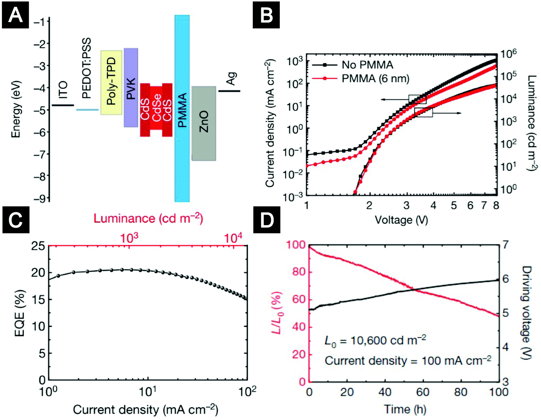 | ||
| Fig. 13 Multilayer QLEDs with an insulting layer between the QD layer and the ZnO ETL. (A) Flat-band energy level diagram. (B) Current density and luminance versus voltage characteristics for QLEDs without or with the PMMA layer. (C) EQE versus current density and luminance for the device with the best efficiency. (D) Stability data for a QLED device (L, luminance). Figures reprinted with permission from ref. 18. Copyright 2014 Macmillan Publishers Limited. | ||
For QLEDs based on alternative QD emitters with relatively low electron affinity, such as CuInS, CuInGaS or ZnCuInS QDs, the band structure of ZnO ETLs needs to be tailored to improve electron injection. Alloying provides an effective approach to tune the electronic structures and properties of ZnO nanocrystals. For example, Kim et al. fabricated QLEDs with CuInS, CuInGaS, or ZnCuInS QDs as emitters and ZnxMg1−xO nanocrystals with varied doping concentrations as ETLs.185 The efficiency and maximum brightness of the devices increased substantially when the ratio of Mg in the oxide-nanocrystal ETLs increased from 0 to 10%. The authors suggested that alloying with Mg ions led to a reduced electron injection barrier at the interface of QD/oxide and hence improved device performance.
The idea of using solution-processed oxide CTLs to construct all-inorganic QLEDs is tempting. Currently p-type oxides, such as NiO, or n-type oxides with high work functions, such as WOx and MoO3, are used to replace PEDOT:PSS, one component of the multi-layer polymeric HTLs.186–190 However, the direct contact of QDs with these oxides causes severe quenching of the QD emission. More detailed studies are necessary to guide the control of interfacial interactions between the QDs and the oxide HTLs.
5.3 Perovskite LEDs
Organic–inorganic hybrid perovskites (Fig. 14A), such as CH3NH3PbI3 (MAPbI3) and NH2CH![[double bond, length as m-dash]](https://www.rsc.org/images/entities/char_e001.gif) NH2PbI3 (FAPbI3), can be processed from solutions at low temperatures to form crystalline direct-bandgap semiconductor films. Hybrid perovskite films may exhibit high photoluminescence quantum efficiency and good charge mobility, making them promising for electroluminescence applications.191–193 One unique feature of perovskite emission is that the efficiency rises with increasing excitation level, which is different from that of the QDs or organic materials. Nevertheless, the stability issues of hybrid perovskite materials, for example, ion migration under a high electric field, need to be addressed to improve the LED lifetime.
NH2PbI3 (FAPbI3), can be processed from solutions at low temperatures to form crystalline direct-bandgap semiconductor films. Hybrid perovskite films may exhibit high photoluminescence quantum efficiency and good charge mobility, making them promising for electroluminescence applications.191–193 One unique feature of perovskite emission is that the efficiency rises with increasing excitation level, which is different from that of the QDs or organic materials. Nevertheless, the stability issues of hybrid perovskite materials, for example, ion migration under a high electric field, need to be addressed to improve the LED lifetime.
 | ||
| Fig. 14 (A) A single unit cell of an ABX3 perovskite crystal, where A is methylammonium or formamidinium, B is Pb and X is I, Br or Cl. (B) Device structure of the first room-temperature perovskite LED. (C) A cross-sectional TEM image showing the architecture of the perovskite LED with PEI modified ZnO nanocrystals as ETLs. (D) Flat-band energy level diagram of the perovskite LED with self-organized multiple quantum wells as emitters and PEI modified ZnO nanocrystals as ETLs. (A and B) Reprinted with permission from ref. 192. Copyright 2014 Macmillan Publishers Limited. (C) Reprinted with permission from ref. 193. Copyright 2015 Wiley-VCH. (D) Reprinted with permission from ref. 23. Copyright 2016 Macmillan Publishers Limited. | ||
Room-temperature perovskite electroluminescence was first reported by Tan et al. in 2014192 (Fig. 14B). In the past two years, owing to the rich experience of interfacial engineering gained from other solution-processed LEDs, the EQEs of perovskite LEDs have improved dramatically, from 0.78% to 11.7%.23,192–195 The key to achieving high-efficiency perovskite electroluminescence is integrating perovskite films with good emissive properties and full surface coverage into a LED structure, which can confine the injected charges within the perovskite layer to allow efficient radiative decay. For the 3D perovskite materials, such as MAPbI3 and FAPbI3, the formation of perovskite films is known to be very sensitive to the surface properties of the underlying layers. Our group employed PEI molecules to modify the surfaces of ZnO-nanocrystal films (Fig. 14C).193 This interfacial engineering approach provided a high-energy hydrophilic surface to facilitate formation of high-quality perovskite thin films. Furthermore, the PEI modification lowered the work function of the ZnO-nanocrystal films, improving electron injection into the hybrid perovskite films. These two merits substantially improved device performance, leading to perovskite LEDs with an EQE of ∼3.5% at a high radiance of 28 W sr−1 m−2 and a low voltage of 2.2 V. In a later work, the ETLs of PEI-modified ZnO-nanocrystal films were inherited by our collaborators, the Wang and Huang group. They introduced perovskite emitters with structures of self-organized multiple quantum wells (MQWs) to replace the 3D perovskite films (Fig. 14D).23 In the perovskite MQW films, the excited states were well confined in the lower-bandgap regions with excellent emissive properties, resulting in very efficient radiative decay. Together with the efficient electron injection provided by the PEI-modified ZnO ETLs, the MQW-based LEDs exhibited a record-high EQE of up to 11.7% and an exceptionally high power conversion efficiency of 5.5% at a current density of 100 mA cm−2.
6. Recent developments of CTLs based on colloidal oxide nanocrystals for solution-processed solar cells
6.1 Organic solar cells
There has been a steady increase in the efficiencies of organic solar cells in the past decade.196–200 Typically, organic solar cells rely on a BHJ structure, blends of electron donors and electron acceptors, to convert incident photons to separated charges. Developments of active layers by designing new materials, e.g. low-bandgap polymers and non-fullerene acceptors, and optimizing BHJ morphologies via various film-deposition methods have been the heart of organic solar cell research.196,199,201–204 As discussed in Section 2, CTLs influence all the elementary processes of organic solar cells. The improved device performance is also largely attributed to the evolution of device structures and interfacial engineering.Currently organic solar cells can be divided into conventional and inverted architectures according to the polarity of charge collection and the direction of charge flow. For both architectures, oxide CTLs have been extensively studied to improve both power-conversion efficiency (PCE) and long-term device stability. Here we focus on oxide CTLs deposited from nanocrystal solutions. We highlight that for the fabrication of top CTLs, oxide nanocrystals in alcohol solutions are highly desirable to minimize damage to the BHJ blends.
As wide-bandgap semiconductors with low work function, n-type TiOx and ZnO films were widely used in organic solar cells as ETLs.60,205–207 The first organic solar cell based on TiOx-nanocrystal ETLs was reported by Yang and co-workers.208 In the early studies, it was shown that a high density of trap states in TiOx significantly affected device performance.209,210 To solve this problem, several strategies were proposed to modify the TiOx ETLs.208,211,212 For example, Choy and co-workers demonstrated that electronic properties of the TiOx-nanocrystal films could be improved by incorporating metal (Au or Ag) nanoparticles.212 Under 560–600 nm illumination, plasmon excited hot electrons in the Au nanoparticles were injected into TiOx films to fill the traps, resulting in significantly improved device performance. Doping TiOx nanocrystals was another effective strategy to improve the interfacial contact properties. For example, Cs2CO3 has been used to dope the TiOx nanocrystals, resulting in increased film conductivity and better contact properties between the ETLs and the metal cathode.208 In a follow-up work, Yang and co-workers systematically investigated organic solar cells using ETLs deposited from pure TiOx nanocrystals, Cs-doped TiOx nanocrystals and ZnO nanocrystals.213 They found that even after UV illumination, the resistance of the device based on pure TiOx nanocrystals was larger than that of the devices based on Cs-doped TiOx and ZnO nanocrystals.
The most widely used ZnO nanocrystals in organic solar cells are synthesized via hydrolysis under basic conditions. These ZnO nanocrystals can be dispersed in alcoholic solvents and thereby can be used as either top ETLs in the conventional structure or bottom ETLs in the inverted structure.214–217 Jen and co-workers firstly employed ZnO nanocrystals to modify the ITO substrates and developed inverted organic solar cells with significantly improved environmental stability.214 Ackermann and co-workers employed ZnO-nanocrystal films as top ETLs in a conventional structure and systematically investigated the relationship between the optical, morphological and electronic properties of the ZnO ETLs and device performance.218 They suggested that the significantly improved device performance was mainly due to the hole blocking properties of ZnO-nanocrystal ETLs in combination with the reduced contact resistance and interfacial recombination of photo-generated charges (Fig. 15A).
 | ||
| Fig. 15 Organic solar cells with ZnO nanocrystals as ETLs. (A) An organic solar cell with the conventional structure: ZnO-nanocrystal films as top ETLs. (B) Flat-band energy level diagram of a tandem organic solar cell with PEDOT:PSS and ZnO nanocrystals as ICL. (C) An organic solar cell with an inverted structure: fullerene-SAM modified ZnO nanocrystal films as bottom ETLs. (A) Reprinted with permission from ref. 218. Copyright 2014 Wiley-VCH. (B) Reprinted with permission from ref. 221. Copyright 2012 Macmillan Publishers Limited. (C) Reprinted with permission from ref. 230. Copyright 2008 American Institute of Physics. | ||
Controllable doping generates ZnO nanocrystals with tuneable optoelectronic properties. In a recent work, Ackermann and co-workers reported a modified protocol for the synthesis of colloidal AZO nanocrystals.215 Highly conductive AZO-nanocrystal ETLs with low surface roughness were obtained even at a low annealing temperature of 80 °C. The highly conductive ETLs not only improved the compatibility of organic solar cells with large-scale solution processing but also opened new opportunities for efficient coloured solar cells. Colour tuning from green to yellow could be achieved by using AZO with different thicknesses as optical spacers.
In addition to single-junction organic solar cells, colloidal ZnO nanocrystals were also used to construct interconnecting layers (ICLs) and minimize loss of open-circuit voltage (VOC) in tandem solar cells.55,219–221 ICLs are sandwiched by two organic solar cell stacks and act as the charge recombination zone. ICLs generally consist of a p-type HTL and an n-type ETL, serving to shift vacuum level via alignment of the Fermi levels.205,222 ZnO-nanocrystal layers with high conductivity can be obtained by low-temperature deposition procedures, which is desirable to minimize morphological changes of active layers used in bottom cells. By employing ZnO nanocrystal/PEDOT:PSS as the ICLs, Yang and co-workers demonstrated two-junction tandem solar cells with high PCEs of 8.6% and 10.6% (Fig. 15B).219,221 In this tandem device, the VOC was close to the sum of VOC of two single junction cells with a negligible loss of ∼0.03 V. ICLs based on ZnO nanocrystals were also efficient for triple-junction tandem solar cells. By inserting two ICLs comprising ZnO nanocrystals, triple-junction polymer solar cells with a PCE of over 11% were fabricated.223 Moreover, ZnO nanocrystals can form ideal ICLs not only with PEDOT:PSS but also with other materials, e.g. conjugated polyelectrolyte layers. Heeger and co-workers demonstrated a tandem device with a PCE of 8.6% based on the ZnO nanocrystals/conjugated polyelectrolyte ICLs.224 Recently, a higher PCE of 11.3% was achieved by incorporating highly self-doped conjugated polyelectrolytes and ZnO nanocrystals as the ICLs.225
Despite the success of applying colloidal ZnO nanocrystals in single-junction and tandem organic solar cells, a major challenge lies in how to control intragap states induced by surface defects. It has been reported that surface defects of ZnO nanocrystals caused significant photocurrent loss and degraded charge selectivity of the cathode interface.226,227 Prosa et al. showed that the release of oxygen chemisorbed onto the surfaces of ZnO nanocrystals under UV irradiation caused photo-induced shunts, resulting in reduced charge selectivity at the cathode interface.228 This process represents an issue for the long-term photo-stability of organic solar cells. Riedl and co-workers showed that photo-induced shunting is a general phenomenon in neat and doped ZnO-based ETLs regardless of whether they are deposited from nanoparticle solutions or by vacuum deposition.229 Several strategies to passivate the surface defects of ZnO-nanocrystal ETLs have been proposed. For example, Jen and co-workers introduced fullerene-based SAMs to avoid direct contact of ZnO nanocrystals with active layers (Fig. 15C).230 Coordination polymers such as poly(ethylene oxide) (PEO) and poly(ethylene glycol) (PEG) were also used to passivate surface defects of ZnO nanocrystals, leading to improved device performance.231–233 So and co-workers showed that UV-ozone treatment efficiently passivated the defect states of ZnO nanocrystals, as indicated by the suppression of defect emission in the photoluminescence measurements.227 In a recent work, we developed a facial EDT treatment to modulate the intragap states of ZnO-nanocrystal films. The covalent bonding of EDT molecules onto ZnO nanocrystals removed a large fraction of the surface defects and introduced a new intragap band, resulting in enhanced electron transport and minimized interfacial bimolecular recombination loss of the resulting solar cells.19 In addition, the well-passivated ZnO nanocrystals were less susceptible to oxygen and water molecules and hence further improved the ambient stability of obtained devices.
HTLs based on high work-function and n-type oxide nanocrystals, such as MoOx and WOx, have also been explored for organic solar cells.156,234–236 For example, Lee et al. developed a facile approach to synthesize MoOx nanocrystals based on a microwave-assisted method.234 The devices with MoOx-nanocrystal HTLs exhibited PCEs comparable to those of devices with PEDOT:PSS HTLs. In a recent report, low-temperature solution-processed WO3 nanocrystals were employed as HTLs in organic solar cells by Brabec and co-workers.235 The small WO3 nanocrystals were stabilized in alcohol-based solvents. Smooth WO3-nanocrystal films were obtained after a mild thermal annealing process (80 °C for 5 min), making them compatible with conventional and inverted organic solar cells. HTLs based on V2O5 nanocrystals and mixed-oxide nanocrystals of WO3 and V2O5 have also been introduced to improve the device performance.236 It was shown that the mixed oxide nanocrystals could effectively suppress the leakage current and enhance optical absorption, resulting in more efficient and stable devices.
Solution-processed p-type NiOx films with high work function can function as hole transporting and electron blocking layers simultaneously in organic solar cells.237,238 Recently, we applied pure NiO nanocrystals synthesized by the ligand-protection strategy to the fabrication of HTLs.25 UV-ozone treatment was used to remove the insulating surface ligands and increase the work function of NiO films (Fig. 16A–D). The devices with NiO-nanocrystal HTLs exhibited an average PCE of 6.1%. In contrast, the average PCE for the devices with PEDOT:PSS as HTLs was 5.0%. In a recent report, Choy and co-workers reported a novel approach for the synthesis of nonstoichiometric NiOx nanocrystals.24 After carefully controlled calcination (270 °C for 2 h) in air, the obtained dark-black NiOx nanocrystals were well dispersed in water to form a stable solution. Even without any post-deposition treatment, the HTLs based on NiOx nanocrystals offered a high work function of 5.25 eV, providing excellent contact for most donor materials in organic solar cells (Fig. 16E and F).
 | ||
| Fig. 16 P-type NiOx nanocrystals and their application as HTLs in organic solar cells. (A) A typical TEM image of the colloidal NiO nanocrystals synthesized by the ligand-protecting method. (B) UPS spectrum of the NiO-nanocrystal HTL. (C) Device structure of organic solar cells with NiO-nanocrystal HTLs and (D) the corresponding J–V curves of the devices. (E) A typical TEM image of the NiOx nanoparticles synthesized by the chemical precipitation method and (F) energy-level diagram of the NiOx-nanocrystal HTL without any post-deposition treatment. (A–D) Reprinted with permission from ref. 25. Copyright 2014 American Chemical Society. (E–F) Reprinted with permission from ref. 24. Copyright 2015 Wiley-VCH. | ||
6.2 QDSCs
Colloidal QDs are attractive for solar cells because of the unique combination of solution-processable characteristics, size-dependent electronic structure, excellent absorption in the visible and infrared region, and potential multi-exciton generation.239–242 In the early stages, QDSCs adopted the Schottky structure, in which QDs were sandwiched between ITO and a low-work-function metal, such as Al and Mg.243–246 However, the Schottky-structured devices suffered from low VOC due to Fermi-level pinning at the Schottky interfaces, as well as inefficient carrier collection because most of the photo-excitations occurred at the regions away from the junction side. The evolution of a Schottky structure to a depleted-heterojunction device with n-type metal oxides as ETLs effectively increased the built-in electric field, giving rise to much improved device performance.239,247 In recent years, the PCEs of QDSCs have shown steady improvements (Fig. 17A), owing to both surface engineering of QDs and optimization of oxide ETLs.22,241,245,247–254 The structure of the device with the highest certified PCE of 10.6% is shown in Fig. 17B. For this device, ZnO-nanocrystal films were used as ETLs.22 | ||
| Fig. 17 (A) Progression of the PCE of QDSCs over time (ref. 22, 245 and 247–252). The PCEs of QDSCs with depleted-heterojunction structures are certified values. (B) Device architecture of the QDSC achieving the highest certified PCE to date. (B) Adapted with permission from ref. 22. Copyright 2016 American Chemical Society. | ||
The compositions and surface coordination states of QDs, which heavily rely on the synthesis, purification and processing procedures, have significant impacts on carrier mobility, defect density, as well as doping density of the QD films. Exquisite modulations of synthetic and purification procedures are important for improving the performance of QDSCs.254–256 Ligand engineering of QDs can effectively reduce defect density and suppress carrier recombination in the QD films, as well as tune the absolute energy levels. For example, halide ligands were explored for passivation of surface defects, leading to QD films with higher carrier mobility and thereby much improved device performance.250 The Bawendi group showed that the ligand-induced surface dipoles could influence the absolute energy levels of QD films.117,251 This finding made it appealing to tailor the band energy alignment of the QD layers with carefully engineered ligands.
For heterojunction QDSCs, the n-type oxide layer is critical to determine the thickness of the depletion region in the QD layer, the built-in voltage, as well as electron extraction and transport. In the early stages, TiO2 paste composed of nanocrystals with sizes of ∼20 nm and carrier density of ∼1016 cm−3 was utilized for ETL fabrication.241 A PCE of over 5% was achieved. Both the VOC and the short-circuit current (JSC) were enhanced compared to the device with Schottky structure. For the heterojunction QDSCs, the energy level offset between the conduction band of TiO2 and QDs should be favourable to facilitate electron extraction from QDs to TiO2 while avoiding excess loss of VOC. For example, the Sargent group studied QDSCs using two types of TiO2 ETLs, one made from nanocrystals with an electron affinity of −3.8 eV and another one deposited by sputtering with an electron affinity of −4.0 eV.257 The parameters of QDSCs based on nanocrystals and sputtered TiO2 thin film were 0.7 and 0.61 V for VOC, 3.5% and 2.7% for PCE, respectively. Given that the electron affinity of QDs used in the devices is ∼3.6 eV, the authors suggested that the energy-level offset of 0.2 eV favoured electron injection from QDs to TiO2 nanocrystal thin films.257 For the sputtered TiO2 thin film, the deeper TiO2 band-edge compromised the VOC.
Interfacial recombination is an important loss pathway that may limit JSC and degrade device efficiency.258 Sargent and co-workers showed that inserting a buffer layer of ZnO onto the surface of TiO2 effectively reduced interfacial recombination, leading to remarkably improved device performance.255 This work suggests that defect centers in TiO2 are one limiting factor for device performance. This work also implies that ZnO may outperform TiO2 in terms of suppressing interfacial recombination.
Currently the majority of the state-of-the-art high-efficiency QDSCs use solution-processed ZnO, e.g. ZnO-nanocrystal films, as ETLs.20,22 The relationship between the properties of ZnO-nanocrystal ETLs and device performance has been investigated by a number of studies. For example, in a QDSC with an inverted structure, effects of varying the doping density of the ZnO-nanocrystal films by illumination were explored.256 Under UV illumination, the absorbed gas molecules, for example O2, on the surfaces of ZnO nanocrystals were removed, resulting in enhanced doping density. Consequently, an additional portion of the depletion region was formed within the hole accepting PbS layer. These effects led to a transition from excitonic behavior to p–n behavior in the device, leading to enhanced charge generation and extraction. In another work, Azmi and co-workers applied the EDT surface passivation method developed by our group to the ZnO-nanocrystal ETLs used in QDSCs.259 They confirmed that the intragap trap states originating from the notorious oxygen-deficient surface states of the ZnO nanocrystals were effectively removed after the EDT treatment. This treatment suppressed interfacial charge recombination at the QD/ETL heterojunction and the PCE was improved from 9.45 to 10.26%. Very recently, Kim et al. showed that addition of organic molecules with strong dipole moment decreased the work function of the ZnO layer, giving rise to increased built-in voltage and better device performance.20 As a result, a remarkable PCE of 10.7% was obtained.
6.3 Perovskite solar cells
Metal halide perovskite solar cells have attracted worldwide attention in recent years due to their high efficiencies and low processing cost.260–266 Owing to the rapid developments of perovskite materials, film deposition and processing and interfacial engineering, the efficiencies of perovskite solar cells have rocketed from the first reported 3.8% to a certified 22.1% over the past few years. Some recent works, such as using cesium ions along with formamidinium cations in lead bromide–iodide cells and two-dimensional Ruddlesden–Popper perovskite solar cells, have shed light on addressing critical factors of thermal- and photo-stability under operating conditions.267,268Initial studies of perovskite solar cells focused on a device structure similar to dye-sensitized solar cells with mesoporous TiO2 or Al2O3 as the scaffolds.6,269 High temperature (450–500 °C) sintered compact TiO2 layers were often used. Further investigation revealed that perovskite materials exhibited ambipolar charge transport and long charge diffusion length, resulting in the success of perovskite solar cells with simplified planar heterojunction (PHJ) structures, in which the perovskite layer was sandwiched between ETL and HTL.270–273 Various CTLs developed for other solution-processed optoelectronics were demonstrated to be suitable for perovskite solar cells. Among them, CTLs based on colloidal oxide nanocrystals showed great potential. Depending on selective charge extraction and transport properties of the bottom contacts, the PHJ solar cells can be further divided into two sub-categories, conventional (n–i–p) and inverted (p–i–n) structure.274 In this section, we will discuss a few relevant examples.
The first PHJ perovskite solar cell developed by Snaith and co-workers was based on high-temperature-sintered compact TiO2 ETLs by gradually decreasing the thickness of Al2O3 scaffolds used in mesoporous devices.6 By employing high-conductivity yttrium-doped TiO2 nanocrystals as ETLs, Yang and co-workers demonstrated one of the most efficient planar devices based on TiO2 ETLs.263 The yttrium doping increased the conductivity of TiO2-nanocrystal films from 6 × 10⁻⁶ to 2 × 10⁻⁵ S cm−1 and significantly improved charge transport in the devices. By further reducing the work function of ITO substrates with PEIE and controlling the humidity of the annealing atmosphere, planar devices with the best PCE of 19.3% and an average PCE of 16.6% were obtained. In addition to TiO2 nanocrystals, ZnO nanocrystals were also employed as ETLs in conventional planar perovskite solar cells. Liu et al. first introduced ZnO nanocrystals as the ETLs for the fabrication of efficient perovskite solar cells at low temperatures (Fig. 18A).275 Highly conductive crystalline SnO2 and Zn2SnO4 (ZSO) nanocrystals were also used as efficient ETLs in conventional PHJ perovskite solar cells.276,277 For example, Rao et al. employed SnO2 nano-colloids to deposit ETLs for PHJ perovskite solar cells.278 Compared to the TiO2, the SnO2 ETLs exhibited higher mobility, resulting in improved photocurrent and device performance. Recently, Seok and co-workers fabricated PHJ perovskite solar cells by employing ETLs deposited from highly dispersed ZSO nanocrystal solutions.277,279 A relatively low temperature (100 °C) was sufficient to obtain ZSO-nanocrystal films with high electron mobility. Moreover, due to its low refractive index, the insertion of the ZSO layer further improved the transmittance of substrates in the visible regions. Based on the high-quality ZSO ETLs, flexible perovskite solar cells with a PCE of ∼15% were achieved.277 By further tailoring the energy level and electron transporting properties of ZSO ETLs using nanocrystals with different sizes, the loss of photogenerated electrons was further reduced. An improved PCE of ∼16% was achieved for the devices based on flexible substrates.279
 | ||
| Fig. 18 (A) Conventional device structure of the perovskite solar cell with ZnO nanocrystals as ETL. (B) Device structure of the inverted planar perovskite solar cell with a ZnO-nanocrystal layer between the PCBM layer and the electrode. (C) Normalized PCE characteristics of the devices as a function of exposure time in air. The inset indicates no degradation of the PCEs when the un-encapsulated device was tested in air under constant illumination for 6 h. (D) Device structure of the perovskite solar cell with NiOx and ZnO as HTL and ETL, respectively. (A) Reprinted with permission from ref. 275. Copyright 2014 Macmillan Publishers Limited. (B and C) Reprinted with permission from ref. 17. Copyright 2014 Tsinghua University Press and Springer. (D) Reprinted with permission from ref. 294. Copyright 2014 Macmillan Publishers Limited. | ||
Currently a critical issue at the interfaces of oxide/perovskite is the lack of control over the sensitive surface states of the oxide nanocrystals. For example, it was shown that oxygen vacancy due to the light-induced desorption of surface absorbed oxygen in TiOx films accounted for poor stability of TiO2-based devices.280 For devices based on ZnO ETLs, surface hydroxyl groups and acetate ligands at the surfaces of oxide nanocrystals may cause unwanted reactions with perovskite films, degrading the stability of perovskite solar cells. The intragap states of the oxide-nanocrystal films can lead to charge accumulation at the cathode interfaces and generate anomalous hysteresis in the J–V curves.281,282 Further efforts are necessary to investigate the surface passivation of oxide-nanocrystal ETLs for perovskite solar cells.
To solve the hysteresis issue of perovskite solar cells, one feasible approach is to use the inverted planar device structure (p–i–n structure). It was shown that fullerene-based ETLs with no dangling bonds or surface states, such as (6,6)-phenyl C61-butyric acid methyl ester (PC61BM) and indene-C60 bisadduct (ICBA), could efficiently suppress hysteresis, leading to improved device performance.283 However, the PC61BM films cannot form stable contact with the low-function metal electrodes. Inserting additional buffer layers between PC61BM and the cathode electrodes was essential to improve the device efficiency and stability. Snaith and co-workers firstly modified the cathode interface with a TiOx layer to fabricate air-stable inverted PHJ perovskite solar cells.284 However, the obtained devices needed to be activated under constant light illumination for several minutes to obtain high PCEs. Moreover, the annealing temperature of ∼130 °C for TiOx films caused decomposition of the underneath perovskite layer. To preserve the superior electronic properties of perovskites, we introduced room-temperature deposited ZnO-nanocrystal interlayers between PC61BM and metal electrodes (Fig. 18B).17 The obtained devices exhibited a significantly enhanced PCE of 15.9% and excellent air stability, while the control devices without ZnO-nanocrystal layers degraded utterly after exposure in air for 30 min (Fig. 18C). In addition to ZnO, highly conductive AZO-, ZSO- or SnO2-nanocrystal films were used to achieve thicker buffer layers between PC61BM and metal electrodes.285–287 Moreover, it has been demonstrated that thick oxide-nanocrystal films were effective in terms of protecting the underneath perovskite films during the sputtering process of the ITO electrode. Therefore these oxide nanocrystals can be used to fabricate perovskite tandem solar cells.288
One important direction in inverted perovskite solar cells is to achieve stable anode contact by replacing hygroscopic PEDOT:PSS with stable metal oxides. Examples include p-type metal oxides, such as CuOx and NiOx, and n-type metal oxides, such as WOx and MoOx.289–293 It should be noted that processing of perovskite films on these metal oxide films requires careful control due to the fact that complicated interactions between these metal oxides and perovskites often lead to poor film quality. In many cases, a fast crystallization process induced by anti-solvent quenching was found to be beneficial in terms of obtaining high-quality perovskite films. Up to now, NiOx is the most widely investigated HTL in inverted perovskite solar cells. In a recent work by You et al., inverted PHJ perovskite solar cells with NiO HTLs and ZnO-nanocrystal ETLs were fabricated (Fig. 18D).294 These devices showed significantly improved stability against water and oxygen degradation, i.e. less than 10% degradation even after 6 days storage in air without encapsulation. NiO HTLs can also be deposited from nanocrystal solutions.295,296 The devices based on NiO-nanocrystal HTLs exhibited high reproducibility with the best PCE of 17.6% and an average efficiency of 15.8%. The low processing temperature of the NiO-nanocrystal HTLs enabled the fabrication of flexible perovskite solar cells with a promising PCE of 14.5%.
7. Conclusions and prospects
Colloidal oxide nanocrystals offer a unique combination of excellent low-temperature solution processability, rich and controllable optoelectronic properties and intrinsic stability, which spurred their applications as CTLs for solution-processed solar cells and LEDs (Fig. 19). Fully exploiting the potential of CTLs based on oxide nanocrystals relies on both in-depth understanding of how the properties of CTLs impact device operation, some of which is currently unknown, to guide material design and on-demand development of material chemistry for colloidal oxide nanocrystals, some of which is currently unavailable, to allow processing of CTLs with desirable properties. The following aspects shall be paid more attention to in future research. | ||
| Fig. 19 Relationship between the chemistry of colloidal oxide nanocrystals, processing and properties of CTLs and device performance of solution-processed LEDs and solar cells. | ||
(i) Ligand chemistry of colloidal oxide nanocrystals. Knowledge of the ligand chemistry of colloidal oxide nanocrystals is surprisingly scarce despite the fact that surface tuning and modification are imperative for their CTL applications. As-synthesized oxide nanocrystals are often ill-suited for CTL applications. For example, weak-binding ligands used to stabilize oxide nanocrystals in solutions tend to dissociate from the nanocrystal surfaces during film processing and device operation, leaving unpassivated surfaces. The high-reactivity surfaces of oxide nanocrystals make the properties of CTLs very sensitive to environments, processing and operational history, which may deteriorate device stability.
We suggest that ligands with strong anchoring groups to facilitate their tight binding onto surfaces of oxide nanocrystals shall be used to lower surface activity and improve stability of the CTL films. The concept of entropy ligand is likely to be a key guideline to meet the demands of both stability of colloidal oxide nanocrystals in solution and charge transport of their corresponding CTLs. It is also possible to further modify the properties of oxide-nanocrystal CTLs by judicious molecular design of functional ligands.
Currently, establishing a link between surface structure of oxide nanocrystals and electronic/transport properties of the corresponding CTLs remains a crucial open question in this field. We highlight that investigations on ligand chemistry may provide unique opportunities to achieve complete surface passivation of the oxide nanocrystals, providing powerful tools to understand and manipulate the intragap states of the corresponding oxide CTLs. Techniques that have been successful in characterizing the intragap states of other semiconductors, such as thermal admittance spectroscopy, deep-level transient spectroscopy, drive-level capacitance profiling and photo-thermal deflection spectroscopy, may be useful in quantifying the intragap states of the oxide-nanocrystal CTLs.
(ii) Synthetic chemistry of p-type oxide nanocrystals. Up to now, the synthesis of NiO nanocrystals is one of the few examples for p-type oxide nanocrystals applicable as HTLs. Synthetic chemistry of NiO nanocrystals is not as mature as that of n-type oxide nanocrystals. Our studies indicated that the extinction coefficient of NiO-nanocrystal films was about one order of magnitude larger than that of other oxide-nanocrystal CTLs, such as ZnO-nanocrystal films, which may cause unneglectable absorption of photons. More exquisite control over the band structure, carrier density, intragap states, stoichiometry and optical properties of the NiO-nanocrystal HTLs shall be pursued in the future. It is also of interest to develop the synthetic chemistry of other p-type oxide nanocrystals, such as the ternary Cu(I) delafossite oxides.
(iii) In-depth understanding of interactions between oxide-nanocrystal CTLs and active layers. Detailed mechanistic studies on interactions between oxide-nanocrystal CTLs and active layers under operational conditions are lacking despite the extensive practice of applying oxide nanocrystals as CTLs in solution-processed LEDs and solar cells. For example, quenching of excitons formed in the QDs by the adjacent oxide CTLs has been identified as one critical factor that limits device performance. However, quenching mechanisms under operational conditions have not been fully disclosed. In our laboratory, preliminary studies on the photoluminescence of QDs in contact with oxide-nanocrystal films showed that several quenching mechanisms, including photo-induced charge separation and charging of QDs due to interfacial charge transfer and energy transfer, were involved depending on the properties of both CTLs and QDs. Moreover, electric field and electric current should be taken into consideration when interpreting the quenching mechanism under electrically driven conditions. For instance, the electric field in the QD layer can modify the radiative recombination rate through spatial separation of the electron and the hole. Multiple techniques, including single-dot photoluminescence or electroluminescence spectroscopy, electrostatic force microscopy, transient-absorption spectroscopy and in situ photoluminescence–electroluminescence spectroscopy, should be combined to gain more comprehensive and rigorous understanding and to provide guidelines to exquisite design of oxide-nanocrystal CTLs beyond the state-of-the-art.
In summary, there is still plenty of room to boost device performance by developing new material chemistry of colloidal oxide nanocrystals and custom-tailoring the properties and processing of CTLs. These efforts shall lead to a new generation of high-performance and all-solution-processed solar cells and LEDs with both ETLs and HTLs based on colloidal oxide nanocrystals, which may revolutionize the current LED and solar-cell industry based on vacuum-deposited crystalline semiconductors. Furthermore, such knowledge can be transferred to the research of other solution-processed devices, such as contact engineering of solution-processed field-effect transistors.
Acknowledgements
This work was financially supported by the National Key Research and Development Program of China (2016YFB0401602 and 2016YFA0204000), the National Natural Science Foundation of China (51522209, 91433204, U1632118, and 21571129), the Fundamental Research Funds for the Central Universities (2015FZA3005), Shanghai Key Research program (16JC1402100), Shanghai International Cooperation Project (16520720700) and the Carl Tryggers Stiftelse and the Swedish Government Strategic Research Area in Materials Science on Functional Materials at Linköping University (Faculty Grant SFO-Mat-LiU # 2009-00971). S. B. is a VINNMER Fellow and Marie Skłodowska-Curie Fellow. We thank Prof. Jianpu Wang (Nanjing Tech University, China), Mr Zhenxing Zhang (Department of Chemistry, Zhejiang University, China), Mr Desui Chen (Department of Chemistry, Zhejiang University, China), Mr Yunzhou Deng (Department of Chemistry, Zhejiang University, China), Mr Yang Liu (School of Materials Science and Engineering, Zhejiang University, China) and Mr Fei Wang (School of Physic Science and Technology, Shanghai Tech University, China) for the assistance in preparing this manuscript.References
- J. H. Burroughes, A. R. Brown and R. N. Marks, Nature, 1990, 347, 539–541 CrossRef CAS.
- R. H. Friend, R. W. Gymer, A. B. Holmes, J. H. Burroughes, R. N. Marks, C. Taliani, D. D. C. Bradley, D. A. Dos Santos, J. L. Bredas, M. Logdlund and W. R. Salaneck, Nature, 1999, 397, 121–128 CrossRef CAS.
- D. J. Noms, C. B. Murray and M. G. Bawendi, J. Am. Chem. Soc., 1993, 115, 8706 CrossRef.
- Y. D. Yin and A. P. Alivisatos, Nature, 2005, 437, 664–670 CrossRef CAS PubMed.
- X. G. Peng, Nano Res., 2009, 2, 425–447 CrossRef CAS.
- M. M. Lee, J. Teuscher, T. Miyasaka, T. N. Murakami and H. J. Snaith, Science, 2012, 338, 643–647 CrossRef CAS PubMed.
- H. S. Kim, C. R. Lee, J. H. Im, K. B. Lee, T. Moehl, A. Marchioro, S. J. Moon, R. Humphry-Baker, J. H. Yum, J. E. Moser, M. Gratzel and N. G. Park, Sci. Rep., 2012, 2, 591 Search PubMed.
- M. Singh, H. M. Haverinen, P. Dhagat and G. E. Jabbour, Adv. Mater., 2010, 22, 673–685 CrossRef CAS PubMed.
- B. J. de Gans, P. C. Duineveld and U. S. Schubert, Adv. Mater., 2004, 16, 203–213 CrossRef CAS.
- K. Hwang, Y. S. Jung, Y. J. Heo, F. H. Scholes, S. E. Watkins, J. Subbiah, D. J. Jones, D. Y. Kim and D. Vak, Adv. Mater., 2015, 27, 1241–1247 CrossRef CAS PubMed.
- C. W. Sele, T. von Werne, R. H. Friend and H. Sirringhaus, Adv. Mater., 2005, 17, 997–1001 CrossRef CAS.
- H. Sirringhaus, T. Kawase, R. H. Friend, T. Shimoda, M. Inbasekaran, W. Wu and E. P. Woo, Science, 2000, 290, 2123 CrossRef CAS PubMed.
- B. H. Kim, M. S. Onses, J. B. Lim, S. Nam, N. Oh, H. Kim, K. J. Yu, J. W. Lee, J. H. Kim, S. K. Kang, C. H. Lee, J. Lee, J. H. Shin, N. H. Kim, C. Leal, M. Shim and J. A. Rogers, Nano Lett., 2015, 15, 969–973 CrossRef CAS PubMed.
- V. Wood, M. J. Panzer, J. Chen, M. S. Bradley, J. E. Halpert, M. G. Bawendi and V. Bulović, Adv. Mater., 2009, 21, 2151–2155 CrossRef CAS.
- J. H. Kim, S. T. Williams, N. Cho, C.-C. Chueh and A. K. Y. Jen, Adv. Energy Mater., 2015, 5, 1401229 CrossRef.
- H. Zheng, Y. N. Zheng, N. L. Liu, N. Ai, Q. Wang, S. Wu, J. H. Zhou, D. G. Hu, S. F. Yu, S. H. Han, W. Xu, C. Luo, Y. H. Meng, Z. X. Jiong, Y. W. Chen, D. Y. Li, F. Huang, J. Wang, J. B. Peng and Y. Cao, Nat. Commun., 2013, 4, 2885 Search PubMed.
- S. Bai, Z. W. Wu, X. J. Wu, Y. Z. Jin, N. Zhao, Z. H. Chen, Q. Q. Mei, X. Wang, Z. Z. Ye, T. Song, R. Y. Liu, S.-t. Lee and B. Q. Sun, Nano Res., 2014, 7, 1749–1758 CrossRef CAS.
- X. L. Dai, Z. X. Zhang, Y. Z. Jin, Y. Niu, H. J. Cao, X. Y. Liang, L. W. Chen, J. P. Wang and X. G. Peng, Nature, 2014, 515, 96–99 CrossRef CAS PubMed.
- S. Bai, Y. Z. Jin, X. Y. Liang, Z. Z. Ye, Z. W. Wu, B. Q. Sun, Z. F. Ma, Z. Tang, J. P. Wang, U. Würfel, F. Gao and F. L. Zhang, Adv. Energy Mater., 2015, 5, 201401606 Search PubMed.
- G. H. Kim, F. P. Garcia de Arquer, Y. J. Yoon, X. Lan, M. X. Liu, O. Voznyy, Z. Y. Yang, F. J. Fan, A. H. Ip, P. Kanjanaboos, S. Hoogland, J. Y. Kim and E. H. Sargent, Nano Lett., 2015, 15, 7691–7696 CrossRef CAS PubMed.
- Y. X. Yang, Y. Zheng, W. R. Cao, A. Titov, J. Hyvonen, J. R. Manders, J. G. Xue, P. H. Holloway and L. Qian, Nat. Photonics, 2015, 9, 259–266 CAS.
- X. Z. Lan, O. Voznyy, F. P. Garcia de Arquer, M. X. Liu, J. X. Xu, A. H. Proppe, G. Walters, F. J. Fan, H. R. Tan, M. Liu, Z. Y. Yang, S. Hoogland and E. H. Sargent, Nano Lett., 2016, 16, 4630–4634 CrossRef CAS PubMed.
- N. N. Wang, L. Cheng, R. Ge, S. T. Zhang, Y. F. Miao, W. Zou, C. Yi, Y. Sun, Y. Cao, R. Yang, Y. Q. Wei, Q. Guo, Y. Ke, M. T. Yu, Y. Z. Jin, Y. Liu, Q. Q. Ding, D. W. Di, L. Yang, G. C. Xing, H. Tian, C. H. Jin, F. Gao, R. H. Friend, J. P. Wang and W. Huang, Nat. Photonics, 2016, 10, 699–704 CrossRef CAS.
- F. Jiang, W. C. H. Choy, X. C. Li, D. Zhang and J. Q. Cheng, Adv. Mater., 2015, 27, 2930–2937 CrossRef CAS PubMed.
- X. Y. Liang, Q. Yi, S. Bai, X. L. Dai, X. Wang, Z. Z. Ye, F. Gao, F. L. Zhang, B. Q. Sun and Y. Z. Jin, Nano Lett., 2014, 14, 3117–3123 CrossRef CAS PubMed.
- N. Espinosa, R. García-Valverde, A. Urbina and F. C. Krebs, Sol. Energy Mater. Sol. Cells, 2011, 95, 1293–1302 CrossRef CAS.
- F. C. Krebs, Sol. Energy Mater. Sol. Cells, 2009, 93, 465–475 CrossRef CAS.
- S. G. Kwon and T. Hyeon, Acc. Chem. Res., 2008, 41, 1696–1709 CrossRef CAS PubMed.
- J. H. Lee, S. Zhang and S. H. Sun, Chem. Mater., 2013, 25, 1293–1304 CrossRef CAS.
- M. Niederberger, Acc. Chem. Res., 2007, 40, 793–800 CrossRef CAS PubMed.
- S. D. Lounis, E. L. Runnerstrom, A. Llordes and D. J. Milliron, J. Phys. Chem. Lett., 2014, 5, 1564–1574 CrossRef CAS PubMed.
- A. Kołodziejczak-Radzimska and T. Jesionowski, Materials, 2014, 7, 2833–2881 CrossRef.
- K. Zilberberg, J. Meyer and T. Riedl, J. Mater. Chem. C, 2013, 1, 4796 RSC.
- C.-C. Chueh, C.-Z. Li and A. K. Y. Jen, Energy Environ. Sci., 2015, 8, 1160–1189 CAS.
- F. Z. Wang, Z. A. Tan and Y. F. Li, Energy Environ. Sci., 2015, 8, 1059–1091 CAS.
- H. Kim, K.-G. Lim and T.-W. Lee, Energy Environ. Sci., 2016, 9, 12–30 CAS.
- S. Chen, J. R. Manders, S.-W. Tsang and F. So, J. Mater. Chem., 2012, 22, 24202–24212 RSC.
- K. Wang, C. Liu, T. Y. Meng, C. Yi and X. Gong, Chem. Soc. Rev., 2016, 45, 2937–2975 RSC.
- Z. Q. Liang, Q. F. Zhang, L. Jiang and G. Z. Cao, Energy Environ. Sci., 2015, 8, 3442–3476 CAS.
- G. Yang, H. Tao, P. L. Qin, W. J. Ke and G. J. Fang, J. Mater. Chem. A, 2016, 4, 3970–3990 CAS.
- W. C. Choy and D. Zhang, Small, 2016, 12, 416–431 CrossRef CAS PubMed.
- W. Yin, L. J. Pan, T. B. Yang and Y. Y. Liang, Molecules, 2016, 21, 837 CrossRef PubMed.
- W. B. Yan, S. Y. Ye, Y. L. Li, W. H. Sun, H. X. Rao, Z. W. Liu, Z. Q. Bian and C. H. Huang, Adv. Energy Mater., 2016, 6, 1600474 CrossRef.
- W. K. Bae, Y. S. Park, J. Lim, D. Lee, L. A. Padilha, H. McDaniel, I. Robel, C. Lee, J. M. Pietryga and V. I. Klimov, Nat. Commun., 2013, 4, 2661 Search PubMed.
- C. Javaux, B. Mahler, B. Dubertret, A. Shabaev, A. V. Rodina, L. EfrosAl, D. R. Yakovlev, F. Liu, M. Bayer, G. Camps, L. Biadala, S. Buil, X. Quelin and J. P. Hermier, Nat. Nanotechnol., 2013, 8, 206–212 CrossRef CAS PubMed.
- B. S. Mashford, M. Stevenson, Z. Popovic, C. Hamilton, Z. Zhou, C. Breen, J. Steckel, V. Bulovic, M. Bawendi, S. Coe-Sullivan and P. T. Kazlas, Nat. Photonics, 2013, 7, 407–412 CrossRef CAS.
- K. Tvrdy, P. A. Frantsuzov and P. V. Kamat, Proc. Natl. Acad. Sci. U. S. A., 2011, 108, 29–34 CrossRef CAS PubMed.
- J. M. Caruge, J. E. Halpert, V. Bulovic and M. G. Bawendi, Nano Lett., 2006, 6, 2991–2994 CrossRef CAS PubMed.
- L. A. Pettersson, L. S. Roman and O. Inganäs, J. Appl. Phys., 1999, 86, 487 CrossRef CAS.
- F. Gao, Loss Mechanisms in Bulk Heterojunction Organic Photovoltaics, University of Cambridge, 2011 Search PubMed.
- B. A. MacLeod, N. E. Horwitz, E. L. Ratcliff, J. L. Jenkins, N. R. Armstrong, A. J. Giordano, P. J. Hotchkiss, S. R. Marder, C. T. Campbell and D. S. Ginger, J. Phys. Chem. Lett., 2012, 3, 1202–1207 CrossRef CAS PubMed.
- M. T. Greiner and Z.-H. Lu, NPG Asia Mater., 2013, 5, e55 CrossRef CAS.
- F. X. Xie, W. C. Choy, C. D. Wang, X. C. Li, S. Q. Zhang and J. J. Hou, Adv. Mater., 2013, 25, 2051–2055 CrossRef CAS PubMed.
- T. Stubhan, N. Li, N. A. Luechinger, S. C. Halim, G. J. Matt and C. J. Brabec, Adv. Energy Mater., 2012, 2, 1433–1438 CrossRef CAS.
- S. Bai, M. T. Cao, Y. Z. Jin, X. L. Dai, X. Y. Liang, Z. Z. Ye, M. Li, J. P. Cheng, X. Z. Xiao, Z. W. Wu, Z. H. Xia, B. Q. Sun, E. Wang, Y. Q. Mo, F. Gao and F. L. Zhang, Adv. Energy Mater., 2014, 4(6), 1301460 CrossRef.
- H. Liu, J. Tang, I. J. Kramer, R. Debnath, G. I. Koleilat, X. Wang, A. Fisher, R. Li, L. Brzozowski, L. Levina and E. H. Sargent, Adv. Mater., 2011, 23, 3832–3837 CrossRef CAS PubMed.
- J. A. Ayllon and M. Lira-Cantu, Appl. Phys. A: Mater. Sci. Process., 2008, 95, 249–255 CrossRef.
- J. Meyer, S. Hamwi, M. Kroger, W. Kowalsky, T. Riedl and A. Kahn, Adv. Mater., 2012, 24, 5408–5427 CrossRef CAS PubMed.
- S. Chandra and M. N. Kamalasanan, Thin Solid Films, 1996, 288, 112–115 CrossRef.
- Y. M. Sun, J. H. Seo, C. J. Takacs, J. Seifter and A. J. Heeger, Adv. Mater., 2011, 23, 1679–1683 CrossRef CAS PubMed.
- Y. M. Sun, C. J. Takacs, S. R. Cowan, J. H. Seo, X. Gong, A. Roy and A. J. Heeger, Adv. Mater., 2011, 23, 2226–2230 CrossRef CAS PubMed.
- M. G. Kim, M. G. Kanatzidis, A. Facchetti and T. J. Marks, Nat. Mater., 2011, 10, 382–388 CrossRef CAS PubMed.
- S. Bai, Z. W. Wu, X. L. Xu, Y. Z. Jin, B. Q. Sun, X. J. Guo, S. S. He, X. Wang, Z. Z. Ye, H. X. Wei, X. Y. Han and W. L. Ma, Appl. Phys. Lett., 2012, 100, 203906 CrossRef.
- A. G. Dong, X. C. Ye, J. Chen, Y. J. Kang, T. Gordon, J. M. Kikkawa and C. B. Murray, J. Am. Chem. Soc., 2011, 133, 998–1006 CrossRef CAS PubMed.
- D. V. Talapin, J. S. Lee, M. V. Kovalenko and E. V. Shevchenko, Chem. Rev., 2010, 110, 389–458 CrossRef CAS PubMed.
- C. L. Carnes, J. Stipp, K. J. Klabunde and J. Bonevich, Langmuir, 2002, 18, 1352–1359 CrossRef CAS.
- S. A. El-Safty, M. Khairy, M. Ismael and H. Kawarada, Appl. Catal., B, 2012, 123, 162–173 CrossRef.
- J. P. Wang and N. C. Greenham, Appl. Phys. Lett., 2014, 104, 193111 CrossRef.
- J. Buha, I. Djerdj and M. Niederberger, Cryst. Growth Des., 2007, 7, 113–116 CAS.
- C. Pacholski, A. Kornowski and H. Weller, Angew. Chem., Int. Ed., 2002, 41, 1188–1191 CrossRef CAS PubMed.
- P. D. Cozzoli, A. Kornowski and H. Weller, J. Am. Chem. Soc., 2003, 125, 14539–14548 CrossRef CAS PubMed.
- A. W. Cohn, K. R. Kittilstved and D. R. Gamelin, J. Am. Chem. Soc., 2012, 134, 7937–7943 CrossRef CAS PubMed.
- X. Wang, X. G. Han, S. F. Xie, Q. Kuang, Y. Q. Jiang, S. B. Zhang, X. L. Mu, G. X. Chen, Z. X. Xie and L. S. Zheng, Chem. – Eur. J., 2012, 18, 2283–2289 CrossRef CAS PubMed.
- M. Niederberger, M. H. Bard and G. D. Stucky, J. Am. Chem. Soc., 2002, 124, 13642–13643 CrossRef CAS PubMed.
- Y. F. Chen, M. Kim, G. Lian, M. B. Johnson and X. G. Peng, J. Am. Chem. Soc., 2005, 127, 13331–13337 CrossRef CAS PubMed.
- J. Polleux, N. Pinna, M. Antonietti and M. Niederberger, J. Am. Chem. Soc., 2005, 127, 15595–15601 CrossRef CAS PubMed.
- B. H. Wu, C. Y. Guo, N. F. Zheng, Z. X. Xie and G. D. Stucky, J. Am. Chem. Soc., 2008, 130, 17563–17567 CrossRef CAS PubMed.
- C. T. Dinh, T. D. Nguyen, F. Kleitz and T. O. Do, ACS Nano, 2009, 3, 3737–3743 CrossRef CAS PubMed.
- B. Ludi, M. J. Suess, I. A. Werner and M. Niederberger, Nanoscale, 2012, 4, 1982–1995 RSC.
- G. C. Xi, S. X. Ouyang, P. Li, J. H. Ye, Q. Ma, N. Su, H. Bai and C. Wang, Angew. Chem., Int. Ed., 2012, 51, 2395–2399 CrossRef CAS PubMed.
- K. Fominykh, J. M. Feckl, J. Sicklinger, M. Doblinger, S. Bocklein, J. Ziegler, L. Peter, J. Rathousky, E. W. Scheidt, T. Bein and D. Fattakhova-Rohlfing, Adv. Funct. Mater., 2014, 24, 3123–3129 CrossRef CAS.
- A. Bergerud, R. Buonsanti, J. L. Jordan-Sweet and D. J. Milliron, Chem. Mater., 2013, 25, 3172–3179 CrossRef CAS.
- T. R. Gordon, M. Cargnello, T. Paik, F. Mangolini, R. T. Weber, P. Fornasiero and C. B. Murray, J. Am. Chem. Soc., 2012, 134, 6751–6761 CrossRef CAS PubMed.
- K. Lee, W. S. Seo and J. T. Park, J. Am. Chem. Soc., 2003, 125, 3408–3409 CrossRef CAS PubMed.
- T. Paik, S. H. Hong, E. A. Gaulding, H. Caglayan, T. R. Gordon, N. Engheta, C. R. Kagan and C. B. Murray, ACS Nano, 2014, 8, 797–806 CrossRef CAS PubMed.
- N. Pinna, G. Garnweitner, M. Antonietti and M. Niederberger, J. Am. Chem. Soc., 2005, 127, 5608–5612 CrossRef CAS PubMed.
- D. S. Wang, T. Xie, Q. Peng, S. Y. Zhang, J. Chen and Y. D. Li, Chem. – Eur. J., 2008, 14, 2507–2513 CrossRef CAS PubMed.
- A. Yella, M. N. Tahir, S. Meuer, R. Zentel, R. Berger, M. Panthofer and W. Tremel, J. Am. Chem. Soc., 2009, 131, 17566–17575 CrossRef CAS PubMed.
- Y. W. Jun, M. F. Casula, J. H. Sim, S. Y. Kim, J. Cheon and A. P. Alivisatos, J. Am. Chem. Soc., 2003, 125, 15981–15985 CrossRef CAS PubMed.
- T. J. Trentler, T. E. Denler, J. F. Bertone, A. Agrawal and V. L. Colvin, J. Am. Chem. Soc., 1999, 121, 1613–1614 CrossRef CAS.
- B. Q. Sun and H. Sirringhaus, Nano Lett., 2005, 5, 2408–2413 CrossRef CAS PubMed.
- N. Pinna, G. Neri, M. Antonietti and M. Niederberger, Angew. Chem., Int. Ed., 2004, 43, 4345–4349 CrossRef CAS PubMed.
- I. Bilecka, I. Djerdj and M. Niederberger, Chem. Commun., 2008, 886–888, 10.1039/b717334b.
- J. Polleux, A. Gurlo, N. Barsan, U. Weimar, M. Antonietti and M. Niederberger, Angew. Chem., Int. Ed., 2005, 45, 261–265 CrossRef PubMed.
- I. Olliges-Stadler, J. Stoetzel, D. Koziej, M. D. Rossell, J.-D. Grunwaldt, M. Nachtegaal, R. Frahm and M. Niederberger, Chem. – Eur. J., 2012, 18, 2305–2312 CrossRef CAS PubMed.
- G. Garnweitner, M. Antonietti and M. Niederberger, Chem. Commun., 2005, 397–399 RSC.
- G. V. Jensen, M. Bremholm, N. Lock, G. R. Deen, T. R. Jensen, B. B. Iversen, M. Niederberger, J. S. Pedersen and H. Birkedal, Chem. Mater., 2010, 22, 6044–6055 CrossRef.
- I. Bilecka, P. Elser and M. Niederberger, ACS Nano, 2009, 3, 467–477 CrossRef CAS PubMed.
- Y. F. Yang, Y. Z. Jin, H. P. He, Q. L. Wang, Y. Tu, H. M. Lu and Z. Z. Ye, J. Am. Chem. Soc., 2010, 132, 13381–13394 CrossRef CAS PubMed.
- X. Y. Liang, Y. P. Ren, S. Bai, N. Zhang, X. L. Dai, X. Wang, H. P. He, C. H. Jin, Z. Z. Ye, Q. Chen, L. W. Chen, J. P. Wang and Y. Z. Jin, Chem. Mater., 2014, 26, 5169–5178 CrossRef CAS.
- X. Wang, Y. Z. Jin, H. P. He, F. Yang, Y. F. Yang and Z. Z. Ye, Nanoscale, 2013, 5, 6464–6468 RSC.
- N. Zhang, X. Wang, Z. Z. Ye and Y. Z. Jin, Sci. Rep., 2014, 4, 04353 Search PubMed.
- A. K. Guria and N. Pradhan, Chem. Mater., 2016, 28, 5224–5237 CrossRef CAS.
- N. S. Karan, S. Sarkar, D. D. Sarma, P. Kundu, N. Ravishankar and N. Pradhan, J. Am. Chem. Soc., 2011, 133, 1666–1669 CrossRef CAS PubMed.
- D. Q. Chen, P. Huang, Y. L. Yu, F. Huang, A. P. Yang and Y. S. Wang, Chem. Commun., 2011, 47, 5801–5803 RSC.
- R. Buonsanti, A. Llordes, S. Aloni, B. A. Helms and D. J. Milliron, Nano Lett., 2011, 11, 4706–4710 CrossRef CAS PubMed.
- T. Stubhan, H. Oh, L. Pinna, J. Krantz, I. Litzov and C. J. Brabec, Org. Electron., 2011, 12, 1539–1543 CrossRef CAS.
- A. M. Schimpf, S. T. Ochsenbein, R. Buonsanti, D. J. Milliron and D. R. Gamelin, Chem. Commun., 2012, 48, 9352–9354 RSC.
- E. Della Gaspera, M. Bersani, M. Cittadini, M. Guglielmi, D. Pagani, R. Noriega, S. Mehra, A. Salleo and A. Martucci, J. Am. Chem. Soc., 2013, 135, 3439–3448 CrossRef PubMed.
- E. Della Gaspera, A. S. R. Chesman, J. van Embden and J. J. Jasieniak, ACS Nano, 2014, 8, 9154–9163 CrossRef CAS PubMed.
- B. L. Greenberg, S. Ganguly, J. T. Held, N. J. Kramer, K. A. Mkhoyan, E. S. Aydil and U. R. Kortshagen, Nano Lett., 2015, 15, 8162–8169 CrossRef CAS PubMed.
- M. Saha, S. Ghosh, V. D. Ashok and S. K. De, Phys. Chem. Chem. Phys., 2015, 17, 16067–16079 RSC.
- V. Müller, M. Rasp, G. Štefanić, J. Ba, S. Günther, J. Rathousky, M. Niederberger and D. Fattakhova-Rohlfing, Chem. Mater., 2009, 21, 5229–5236 CrossRef.
- L. De Trizio, R. Buonsanti, A. M. Schimpf, A. Llordes, D. R. Gamelin, R. Simonutti and D. J. Milliron, Chem. Mater., 2013, 25, 3383–3390 CrossRef CAS.
- Y. J. Liu, J. M. Szeifert, J. M. Feckl, B. Mandlmeier, J. Rathousky, O. Hayden, D. Fattakhova-Rohlfing and T. Bein, ACS Nano, 2010, 4, 5373–5381 CrossRef CAS PubMed.
- R. Buonsanti and D. J. Milliron, Chem. Mater., 2013, 25, 1305–1317 CrossRef CAS.
- P. R. Brown, D. Kim, R. R. Lunt, N. Zhao, M. G. Bawendi, J. C. Grossman and V. Bulović, ACS Nano, 2014, 8, 5863–5872 CrossRef CAS PubMed.
- M. L. H. Green, J. Org. Chem., 1995, 500, 127–148 CrossRef CAS.
- J. Owen, Science, 2015, 347, 615–616 CrossRef CAS PubMed.
- N. C. Anderson, M. P. Hendricks, J. J. Choi and J. S. Owen, J. Am. Chem. Soc., 2013, 135, 18536–18548 CrossRef CAS PubMed.
- J. De Roo, I. Van Driessche, J. C. Martins and Z. Hens, Nat. Mater., 2016, 15, 517–521 CrossRef CAS PubMed.
- J. De Roo, Y. Justo, K. De Keukeleere, F. Van den Broeck, J. C. Martins, I. Van Driessche and Z. Hens, Angew. Chem., Int. Ed., 2015, 54, 6488–6491 CrossRef CAS PubMed.
- J. De Roo, F. Van den Broeck, K. De Keukeleere, J. C. Martins, I. Van Driessche and Z. Hens, J. Am. Chem. Soc., 2014, 136, 9650–9657 CrossRef CAS PubMed.
- R. D. Palma, S. Peeters, M. J. Van Bael, H. V. den Rul, K. Bonroy, W. Laureyn, J. Mullens, G. Borghs and G. Maes, Chem. Mater., 2007, 19, 1821–1831 CrossRef.
- E. K. U. Larsen, T. Nielsen, T. Wittenborn, H. Birkedal, T. Vorup-Jensen, M. H. Jakobsen, L. Østergaard, M. R. Horsman, F. Besenbacher, K. A. Howard and J. Kjems, ACS Nano, 2009, 3, 1947–1951 CrossRef CAS PubMed.
- R. Gomes, A. Hassinen, A. Szczygiel, Q. Zhao, A. Vantomme, J. C. Martins and Z. Hens, J. Phys. Chem. Lett., 2011, 2, 145–152 CrossRef CAS.
- M. V. Kovalenko, M. Scheele and D. V. Talapin, Science, 2009, 324, 1417–1420 CrossRef CAS PubMed.
- D. C. Oertel, M. G. Bawendi, A. C. Arango and V. Bulovic, Appl. Phys. Lett., 2005, 87, 213505 CrossRef.
- M. V. Kovalenko, M. I. Bodnarchuk and D. V. Talapin, J. Am. Chem. Soc., 2010, 132, 15124–15126 CrossRef CAS PubMed.
- A. W. Wills, M. S. Kang, A. Khare, W. L. Gladfelter and D. J. Norris, ACS Nano, 2010, 4, 4523–4530 CrossRef CAS PubMed.
- M. V. Kovalenko, M. I. Bodnarchuk, J. Zaumseil, J.-S. Lee and D. V. Talapin, J. Am. Chem. Soc., 2010, 132, 10085–10092 CrossRef CAS PubMed.
- Y. Yang, H. Y. Qin, M. W. Jiang, L. Lin, T. Fu, X. L. Dai, Z. Z. Zhang, Y. Niu, H. J. Cao, Y. Z. Jin, F. Zhao and X. G. Peng, Nano Lett., 2016, 16, 2133–2138 CrossRef CAS PubMed.
- Y. Yang, H. Y. Qin and X. G. Peng, Nano Lett., 2016, 16, 2127–2132 CrossRef CAS PubMed.
- J. P. Wang, Optoelectronic Properties and Memory Effects of ZnO Nanocrystals, University of Cambridge, 2009 Search PubMed.
- L. S. M. Hilgendorff, C. Rothenhöusler and G. Muller, J. Electrochem. Soc., 1998, 145, 3632–3637 CrossRef.
- S. Y. Liu, R. Liu, Y. Chen, S. Ho, J. H. Kim and F. So, Chem. Mater., 2014, 26, 4528–4534 CrossRef CAS.
- J. Zhang, J. T. Wang, Y. Y. Fu, B. H. Zhang and Z. Y. Xie, J. Mater. Chem. C, 2014, 2, 8295–8302 RSC.
- Y. H. Zhou, C. Fuentes-Hernandez, J. Shim, J. Meyer, A. J. Giordano, H. Li, P. Winget, T. Papadopoulos, H. Cheun, J. Kim, M. Fenoll, A. Dindar, W. Haske, E. Najafabadi, T. M. Khan, H. Sojoudi, S. Barlow, S. Graham, J. L. Bredas, S. R. Marder, A. Kahn and B. Kippelen, Science, 2012, 336, 327–332 CrossRef CAS PubMed.
- Y. E. Ha, M. Y. Jo, J. Park, Y.-C. Kang, S. II. Yoo and J. H. Kim, J. Phys. Chem. C, 2013, 117, 2646–2652 CAS.
- Q. B. Pei and Y. Yang, J. Am. Chem. Soc., 1996, 118, 7416–7417 CrossRef CAS.
- H. J. Bolink, E. Coronado, D. Repetto and M. Sessolo, Appl. Phys. Lett., 2007, 91, 223501 CrossRef.
- N. Aizawa, Y. J. Pu, M. Watanabe, T. Chiba, K. Ideta, N. Toyota, M. Igarashi, Y. Suzuri, H. Sasabe and J. Kido, Nat. Commun., 2014, 5, 5756 CrossRef PubMed.
- M. Cai, T. Xiao, E. Hellerich, Y. Chen, R. Shinar and J. Shinar, Adv. Mater., 2011, 23, 3590–3596 CrossRef CAS PubMed.
- L. Ying, C. L. Ho, H. B. Wu, Y. Cao and W. Y. Wong, Adv. Mater., 2014, 26, 2459–2473 CrossRef CAS PubMed.
- M. Sessolo and H. J. Bolink, Adv. Mater., 2011, 23, 1829–1845 CrossRef CAS PubMed.
- S. A. Haque, S. Koops, N. Tokmoldin, J. R. Durrant, J. Huang, D. D. C. Bradley and E. Palomares, Adv. Mater., 2007, 19, 683–687 CrossRef CAS.
- L. Qian, Y. Zheng, K. R. Choudhury, D. Bera, F. So, J. G. Xue and P. H. Holloway, Nano Today, 2010, 5, 384–389 CrossRef CAS.
- M. Sessolo, H. J. Bolink, H. Brine, H. Prima-Garcia and R. Tena-Zaera, J. Mater. Chem., 2012, 22, 4916 RSC.
- E. F. Schubert, T. Gessmann and J. K. Kim, Light Emitting Diodes, John Wiley & Sons, Inc., 2005 Search PubMed.
- T. Chiba, Y.-J. Pu, H. Sasabe, J. Kido and Y. Yang, J. Mater. Chem., 2012, 22, 22769 RSC.
- T. Chiba, Y.-J. Pu and J. Kido, Adv. Mater., 2015, 27, 4681–4687 CrossRef CAS PubMed.
- M. Zhang, S. Hofle, J. Czolk, A. Mertens and A. Colsmann, Nanoscale, 2015, 7, 20009–20014 RSC.
- S. Höfle, A. Schienle, C. Bernhard, M. Bruns, U. Lemmer and A. Colsmann, Adv. Mater., 2014, 26, 5155–5159 CrossRef PubMed.
- Y.-J. Pu, T. Chiba, K. Ideta, S. Takahashi, N. Aizawa, T. Hikichi and J. Kido, Adv. Mater., 2015, 27, 1327–1332 CrossRef CAS PubMed.
- H. Lee, C.-M. Kang, M. Park, J. Kwak and C. Lee, ACS Appl. Mater. Interfaces, 2013, 5, 1977–1981 CAS.
- J. Meyer, R. Khalandovsky, P. Görrn and A. Kahn, Adv. Mater., 2011, 23, 70–73 CrossRef CAS PubMed.
- G. J. Supran, Y. Shirasaki, K. W. Song, J.-M. Caruge, P. T. Kazlas, S. Coe-Sullivan, T. L. Andrew, M. G. Bawendi and V. Bulovic, MRS Bull., 2013, 38, 703–711 CrossRef.
- J. M. Pietryga, Y.-S. Park, J. Lim, A. F. Fidler, W. K. Bae, S. Brovelli and V. I. Klimov, Chem. Rev., 2016, 116, 10513–10622 CrossRef CAS PubMed.
- V. L. Colvin, M. C. Schlamp and A. P. Alivisatos, Nature, 1994, 370, 354–357 CrossRef CAS.
- B. O. Dabbousi, M. G. Bawendi, O. Onitsuka and M. F. Rubner, Appl. Phys. Lett., 1995, 66, 1316–1318 CrossRef CAS.
- M. C. Schlamp, X. G. Peng and A. P. Alivisatos, J. Appl. Phys., 1997, 82, 5837–5842 CrossRef CAS.
- S. Coe, W. K. Woo, M. Bawendi and V. Bulović, Nature, 2002, 420, 800–803 CrossRef CAS PubMed.
- S. Coe-Sullivan, W. K. Woo, J. S. Steckel, M. Bawendi and V. Bulovic, Org. Electron., 2003, 4, 123–130 CrossRef CAS.
- S. Coe-Sullivan, J. S. Steckel, W. K. Woo, M. G. Bawendi and V. Bulovic, Adv. Funct. Mater., 2005, 15, 1117–1124 CrossRef CAS.
- J. S. Steckel, P. Snee, S. Coe-Sullivan, J. P. Zimmer, J. E. Halpert, P. Anikeeva, L. A. Kim, V. Bulovic and M. G. Bawendi, Angew. Chem., Int. Ed., 2006, 45, 5796–5799 CrossRef CAS PubMed.
- P. O. Anikeeva, J. E. Halpert, M. G. Bawendi and V. Bulovic, Nano Lett., 2007, 7, 2196–2200 CrossRef CAS PubMed.
- Y. H. Niu, A. M. Munro, Y. J. Cheng, Y. Tian, M. S. Liu, J. Zhao, J. A. Bardecker, I. Jen-La Plante, D. S. Ginger and A. K. Y. Jen, Adv. Mater., 2007, 19, 3371–3376 CrossRef CAS.
- P. O. Anikeeva, C. F. Madigan, J. E. Halpert, M. G. Bawendi and V. Bulovic, Phys. Rev. B: Condens. Matter Mater. Phys., 2008, 78, 085434 CrossRef.
- P. O. Anikeeva, J. E. Halpert, M. G. Bawendi and V. Bulovic, Nano Lett., 2009, 9, 2532–2536 CrossRef CAS PubMed.
- Q. J. Sun, G. Subramanyam, L. M. Dai, M. Check, A. Campbell, R. Naik, J. Grote and Y. Q. Wang, ACS Nano, 2009, 3, 737–743 CrossRef CAS PubMed.
- L. Qian, Y. Zheng, J. G. Xue and P. H. Holloway, Nat. Photonics, 2011, 5, 543–548 CrossRef CAS.
- J. Kwak, W. K. Bae, D. Lee, I. Park, J. Lim, M. Park, H. Cho, H. Woo, D. Y. Yoon, K. Char, S. Lee and C. Lee, Nano Lett., 2012, 12, 2362–2366 CrossRef CAS PubMed.
- K.-H. Lee, J.-H. Lee, W.-S. Song, H. Ko, C. Lee, J.-H. Lee and H. Yang, ACS Nano, 2013, 7, 7295–7302 CrossRef CAS PubMed.
- K.-H. Lee, J.-H. Lee, H.-D. Kang, B. Park, Y. Kwon, H. Ko, C. Lee, J. Lee and H. Yang, ACS Nano, 2014, 8, 4893–4901 CrossRef CAS PubMed.
- H. B. Shen, W. R. Cao, N. T. Shewmon, C. C. Yang, L. S. Li and J. G. Xue, Nano Lett., 2015, 15, 1211–1216 CrossRef CAS PubMed.
- Y. Gao and X. G. Peng, J. Am. Chem. Soc., 2015, 137, 4230–4235 CrossRef CAS PubMed.
- C. D. Pu and X. G. Peng, J. Am. Chem. Soc., 2016, 138, 8134–8142 CrossRef CAS PubMed.
- Z. A. Peng and X. G. Peng, J. Am. Chem. Soc., 2002, 124, 3343–3353 CrossRef CAS PubMed.
- O. Chen, J. Zhao, V. P. Chauhan, J. Cui, C. Wong, D. K. Harris, H. Wei, H.-S. Han, D. Fukumura and R. K. Jain, Nat. Mater., 2013, 12, 445–451 CrossRef CAS PubMed.
- W. E. Ford, D. Gao, N. Knorr, R. Wirtz, F. Scholz, Z. Karipidou, K. Ogasawara, S. Rosselli, V. Rodin, G. Nelles and F. von Wrochem, ACS Nano, 2014, 8, 9173–9180 CrossRef CAS PubMed.
- J. M. Caruge, J. E. Halpert, V. Wood, V. Bulović and M. G. Bawendi, Nat. Photonics, 2008, 2, 247–250 CrossRef CAS.
- J. W. Stouwdam and R. A. J. Janssen, J. Mater. Chem., 2008, 18, 1889–1894 RSC.
- J.-M. C. Yajie Dong, Z. Zhou, C. Hamilton, J. H. Zoran Popovic, M. Stevenson, G. Liu, V. Bulovic, M. Bawendi, P. T. Kazlas, J. Steckel and S. Coe-Sullivan, SID Int. Symp. Dig. Tech. Pap., 2015, 46, 270–273 Search PubMed.
- H. Zhang, N. Sui, X. Chi, Y. Wang, Q. Liu, H. Zhang and W. Ji, ACS Appl. Mater. Interfaces, 2016, 8, 31385–31391 CAS.
- J.-H. Kim, C.-Y. Han, K.-H. Lee, K.-S. An, W. Song, J. Kim, M. S. Oh, Y. R. Do and H. Yang, Chem. Mater., 2015, 27, 197–204 CrossRef CAS.
- H. T. Nguyen, N. D. Nguyen and S. Lee, Nanotechnology, 2013, 24, 115201 CrossRef PubMed.
- H. T. Nguyen, H. Jeong, J.-Y. Park, Y. H. Ahn and S. Lee, ACS Appl. Mater. Interfaces, 2014, 6, 7286–7291 CAS.
- T. Ding, X. Y. Yang, L. Y. Bai, Y. B. Zhao, K. E. Fong, N. Wang, H. V. Demir and X. W. Sun, Org. Electron., 2015, 26, 245–250 CrossRef CAS.
- X. Y. Yang, Y. Y. Ma, E. Mutlugun, Y. B. Zhao, K. S. Leck, S. T. Tan, H. V. Demir, Q. Y. Zhang, H. J. Du and X. W. Sun, ACS Appl. Mater. Interfaces, 2014, 6, 495–499 CAS.
- S. Bhaumik and A. J. Pal, ACS Appl. Mater. Interfaces, 2014, 6, 11348–11356 CAS.
- F. Deschler, M. Price, S. Pathak, L. E. Klintberg, D. D. Jarausch, R. Higler, S. Huttner, T. Leijtens, S. D. Stranks, H. J. Snaith, M. Atature, R. T. Phillips and R. H. Friend, J. Phys. Chem. Lett., 2014, 5, 1421–1426 CrossRef CAS PubMed.
- Z. K. Tan, R. S. Moghaddam, M. L. Lai, P. Docampo, R. Higler, F. Deschler, M. Price, A. Sadhanala, L. M. Pazos, D. Credgington, F. Hanusch, T. Bein, H. J. Snaith and R. H. Friend, Nat. Nanotechnol., 2014, 9, 687–692 CrossRef CAS PubMed.
- J. P. Wang, N. N. Wang, Y. Z. Jin, J. J. Si, Z. K. Tan, H. Du, L. Cheng, X. L. Dai, S. Bai, H. P. He, Z. Z. Ye, M. L. Lai, R. H. Friend and W. Huang, Adv. Mater., 2015, 27, 2311–2316 CrossRef CAS PubMed.
- M. Yuan, L. N. Quan, R. Comin, G. Walters, R. Sabatini, O. Voznyy, S. Hoogland, Y. Zhao, E. M. Beauregard and P. Kanjanaboos, Nat. Nanotechnol., 2016, 872–877 CrossRef CAS PubMed.
- H. Cho, S.-H. Jeong, M.-H. Park, Y.-H. Kim, C. Wolf, C.-L. Lee, J. H. Heo, A. Sadhanala, N. Myoung and S. Yoo, Science, 2015, 350, 1222–1225 CrossRef CAS PubMed.
- G. Li, V. Shrotriya, J. S. Huang, Y. Yao, T. Moriarty, K. Emery and Y. Yang, Nat. Mater., 2005, 4, 864–868 CrossRef CAS.
- S. H. Park, A. Roy, S. Beaupré, S. Cho, N. Coates, J. S. Moon, D. Moses, M. Leclerc, K. Lee and A. J. Heeger, Nat. Photonics, 2009, 3, 297–302 CrossRef CAS.
- Z. C. He, C. M. Zhong, S. J. Su, M. Xu, H. B. Wu and Y. Cao, Nat. Photonics, 2012, 6, 591–595 Search PubMed.
- S. Li, L. Ye, W. Zhao, S. Zhang, S. Mukherjee, H. Ade and J. Hou, Adv. Mater., 2016, 28, 9423–9429 CrossRef CAS PubMed.
- J. Zhao, Y. Li, G. Yang, K. Jiang, H. Lin, H. Ade, W. Ma and H. Yan, Nat. Energy, 2016, 1, 15027 CrossRef CAS.
- J. Peet, J. Y. Kim, N. E. Coates, W. L. Ma, D. Moses, A. J. Heeger and G. C. Bazan, Nat. Mater., 2007, 6, 497–500 CrossRef CAS PubMed.
- W. C. Zhao, D. P. Qian, S. Q. Zhang, S. S. Li, O. Inganäs, F. Gao and J. H. Hou, Adv. Mater., 2016, 28, 4734–4739 CrossRef CAS PubMed.
- Y. Li, Acc. Chem. Res., 2012, 45, 723–733 CrossRef CAS PubMed.
- Y. Z. Lin, F. W. Zhao, Q. He, L. J. Huo, Y. Wu, T. C. Parker, W. Ma, Y. M. Sun, C. R. Wang and D. B. Zhu, J. Am. Chem. Soc., 2016, 138, 4955–4961 CrossRef CAS PubMed.
- J. Y. Kim, K. Lee, N. E. Coates, D. Moses, T.-Q. Nguyen, M. Dante and A. J. Heeger, Science, 2007, 317, 222–225 CrossRef CAS PubMed.
- A. K. K. Kyaw, X. W. Sun, C. Y. Jiang, G. Q. Lo, D. W. Zhao and D. L. Kwong, Appl. Phys. Lett., 2008, 93, 221107 CrossRef.
- W. J. E. Beek, M. M. Wienk, M. Kemerink, X. N. Yang and R. A. J. Janssen, J. Phys. Chem. B, 2005, 109, 9505–9516 CrossRef CAS PubMed.
- M.-H. Park, J.-H. Li, A. Kumar, G. Li and Y. Yang, Adv. Funct. Mater., 2009, 19, 1241–1246 CrossRef CAS.
- F. J. Lim, K. Ananthanarayanan, J. Luther and G. W. Ho, J. Mater. Chem., 2012, 22, 25057 RSC.
- H. Schmidt, K. Zilberberg, S. Schmale, H. Flügge, T. Riedl and W. Kowalsky, Appl. Phys. Lett., 2010, 96, 243305 CrossRef.
- F.-X. Xie, W. C. H. Choy, W. E. I. Sha, D. Zhang, S. Zhang, X. Li, C.-W. Leung and J. Hou, Energy Environ. Sci., 2013, 6, 3372 CAS.
- D. Zhang, W. C. H. Choy, F. Xie, W. E. I. Sha, X. C. Li, B. F. Ding, K. Zhang, F. Huang and Y. Cao, Adv. Funct. Mater., 2013, 23, 4255–4261 CrossRef CAS.
- J. B. You, C.-C. Chen, L. T. Dou, S. Murase, H.-S. Duan, S. A. Hawks, T. Xu, H. J. Son, L. P. Yu, G. Li and Y. Yang, Adv. Mater., 2012, 24, 5267–5272 CrossRef CAS PubMed.
- S. K. Hau, H.-L. Yip, N. S. Baek, J. Zou, K. O'Malley and A. K.-Y. Jen, Appl. Phys. Lett., 2008, 92, 253301 CrossRef.
- M. Gaceur, S. B. Dkhil, D. Duché, F. Bencheikh, J.-J. Simon, L. Escoubas, M. Mansour, A. Guerrero, G. Garcia-Belmonte, X. Liu, M. Fahlman, W. Dachraoui, A. K. Diallo, C. Videlot-Ackermann, O. Margeat and J. Ackermann, Adv. Funct. Mater., 2016, 26, 243–253 CrossRef CAS.
- R. M. Hewlett and M. A. McLachlan, Adv. Mater., 2016, 28, 3893–3921 CrossRef CAS PubMed.
- Z. Q. Liang, Q. F. Zhang, L. Jiang and G. Z. Cao, Energy Environ. Sci., 2015, 8, 3442–3476 CAS.
- S. B. Dkhil, D. Duché, M. Gaceur, A. K. Thakur, F. B. Aboura, L. Escoubas, J.-J. Simon, A. Guerrero, J. Bisquert, G. Garcia-Belmonte, Q. Y. Bao, M. Fahlman, C. Videlot-Ackermann, O. Margeat and J. Ackermann, Adv. Energy Mater., 2014, 4, 1400805 CrossRef.
- J. B. You, L. Dou, K. Yoshimura, T. Kato, K. Ohya, T. Moriarty, K. Emery, C.-C. Chen, J. Gao, G. Li and Y. Yang, Nat. Commun., 2013, 4, 1446 CrossRef PubMed.
- J. Y. Yuan, J. N. Gu, G. Z. Shi, J. X. Sun, H. Q. Wang and W. L. Ma, Sci. Rep., 2016, 6, 26459 CrossRef CAS PubMed.
- L. T. Dou, J. B. You, J. Yang, C.-C. Chen, Y. J. He, S. Murase, T. Moriarty, K. Emery, G. Li and Y. Yang, Nat. Photonics, 2012, 6, 180–185 CrossRef CAS.
- T. Ameri, G. Dennler, C. Lungenschmied and C. J. Brabec, Energy Environ. Sci., 2009, 2, 347–363 CAS.
- C.-C. Chen, W.-H. Chang, K. Yoshimura, K. Ohya, J. B. You, J. Gao, Z. R. Hong and Y. Yang, Adv. Mater., 2014, 26, 5670–5677 CrossRef CAS PubMed.
- J. Jo, J.-R. Pouliot, D. Wynands, S. D. Collins, J. Y. Kim, T. L. Nguyen, H. Y. Woo, Y. M. Sun, M. Leclerc and A. J. Heeger, Adv. Mater., 2013, 25, 4783–4788 CrossRef CAS PubMed.
- H. Q. Zhou, Y. Zhang, C.-K. Mai, S. D. Collins, G. C. Bazan, T.-Q. Nguyen and A. J. Heeger, Adv. Mater., 2015, 27, 1767–1773 CrossRef CAS PubMed.
- A. Gadisa, Y. Liu, E. T. Samulski and R. Lopez, Appl. Phys. Lett., 2012, 100, 253903 CrossRef.
- S. Chen, C. E. Small, C. M. Amb, J. Subbiah, T.-h. Lai, S.-W. Tsang, J. R. Manders, J. R. Reynolds and F. So, Adv. Energy Mater., 2012, 2, 1333–1337 CrossRef CAS.
- M. Prosa, M. Tessarolo, M. Bolognesi, O. Margeat, D. Gedefaw, M. Gaceur, C. Videlot-Ackermann, M. R. Andersson, M. Muccini, M. Seri and J. Ackermann, ACS Appl. Mater. Interfaces, 2016, 8, 1635–1643 CAS.
- S. Trost, T. Becker, A. Polywka, P. Görrn, M. F. Oszajca, N. A. Luechinger, D. Rogalla, M. Weidner, P. Reckers, T. Mayer and T. Riedl, Adv. Energy Mater., 2016, 6, 1600347 CrossRef.
- S. K. Hau, H.-L. Yip, H. Ma and A. K.-Y. Jen, Appl. Phys. Lett., 2008, 93, 233304 CrossRef.
- S. Y. Shao, K. B. Zheng, T. Pullerits and F. L. Zhang, ACS Appl. Mater. Interfaces, 2013, 5, 380–385 CAS.
- S. B. Jo, J. H. Lee, M. Sim, M. Kim, J. H. Park, Y. S. Choi, Y. Kim, S.-G. Ihn and K. Cho, Adv. Energy Mater., 2011, 1, 690–698 CrossRef CAS.
- T. Hu, F. Li, K. Yuan and Y. W. Chen, ACS Appl. Mater. Interfaces, 2013, 5, 5763–5770 CAS.
- Y.-J. Lee, J. Yi, G. F. Gao, H. Koerner, K. Park, J. Wang, K. Y. Luo, R. A. Vaia and J. W. P. Hsu, Adv. Energy Mater., 2012, 2, 1193–1197 CrossRef CAS.
- T. Stubhan, N. Li, N. A. Luechinger, S. C. Halim, G. J. Matt and C. J. Brabec, Adv. Energy Mater., 2012, 2, 1433–1438 CrossRef CAS.
- J.-S. Huang, C.-Y. Chou and C.-F. Lin, IEEE Electron Device Lett., 2010, 31, 332–334 CrossRef CAS.
- P. Schulz, S. R. Cowan, Z.-L. Guan, A. Garcia, D. C. Olson and A. Kahn, Adv. Funct. Mater., 2014, 24, 701–706 CrossRef CAS.
- Z. C. Zhai, X. D. Huang, M. F. Xu, J. Y. Yuan, J. Peng and W. L. Ma, Adv. Energy Mater., 2013, 3, 1614–1622 CrossRef CAS.
- D. A. Barkhouse, R. Debnath, I. J. Kramer, D. Zhitomirsky, A. G. Pattantyus-Abraham, L. Levina, L. Etgar, M. Gratzel and E. H. Sargent, Adv. Mater., 2011, 23, 3134–3138 CrossRef CAS PubMed.
- L. Etgar, D. Yanover, R. K. Čapek, R. Vaxenburg, Z. S. Xue, B. Liu, M. K. Nazeeruddin, E. Lifshitz and M. Grätzel, Adv. Funct. Mater., 2013, 23, 2736–2741 CrossRef CAS.
- A. G. Pattantyus-Abraham, I. J. Kramer, A. R. Barkhouse, X. H. Wang, G. Konstantatos, R. Debnath, L. Levina, I. Raabe, M. K. Nazeeruddin, M. Gratzel and E. H. Sargent, ACS Nano, 2010, 4, 3374–3380 CrossRef CAS PubMed.
- M. L. Bohm, T. C. Jellicoe, M. Tabachnyk, N. J. Davis, F. Wisnivesky-Rocca-Rivarola, C. Ducati, B. Ehrler, A. A. Bakulin and N. C. Greenham, Nano Lett., 2015, 15, 7987–7993 CrossRef CAS PubMed.
- D. A. Barkhouse, A. G. Pattantyus-Abraham, L. Levina and E. H. Sargent, ACS Nano, 2008, 2, 2356–2362 CrossRef CAS PubMed.
- G. I. Koleilat, L. Levina, H. Shukla, S. H. Myrskog, S. Hinds, A. G. Pattantyus-Abraham and E. H. Sargent, ACS Nano, 2008, 2, 833–840 CrossRef CAS PubMed.
- J. M. Luther, M. Law, M. C. Beard, Q. Song, M. O. Reese, R. J. Ellingson and A. J. Nozik, Nano Lett., 2008, 8, 3488–3492 CrossRef CAS PubMed.
- J. Tang, X. H. Wang, L. Brzozowski, D. A. Barkhouse, R. Debnath, L. Levina and E. H. Sargent, Adv. Mater., 2010, 22, 1398–1402 CrossRef CAS PubMed.
- A. H. Ip, S. M. Thon, S. Hoogland, O. Voznyy, D. Zhitomirsky, R. Debnath, L. Levina, L. R. Rollny, G. H. Carey, A. Fischer, K. W. Kemp, I. J. Kramer, Z. Ning, A. J. Labelle, K. W. Chou, A. Amassian and E. H. Sargent, Nat. Nanotechnol., 2012, 7, 577–582 CrossRef CAS PubMed.
- J. J. Choi, Y.-F. Lim, M. B. Santiago-Berrios, M. Oh, B. R. Hyun, L. F. Sun, A. C. Bartnik, A. Goedhart, G. G. Malliaras, H. D. Abruna, F. W. Wise and T. Hanrath, Nano Lett., 2009, 9, 3749–3755 CrossRef CAS PubMed.
- J. M. Luther, J. Gao, M. T. Lloyd, O. E. Semonin, M. C. Beard and A. J. Nozik, Adv. Mater., 2010, 22, 3704–3707 CrossRef CAS PubMed.
- J. Tang, K. W. Kemp, S. Hoogland, K. S. Jeong, H. Liu, L. Levina, M. Furukawa, X. H. Wang, R. Debnath, D. Cha, K. W. Chou, A. Fischer, A. Amassian, J. B. Asbury and E. H. Sargent, Nat. Mater., 2011, 10, 765–771 CrossRef CAS PubMed.
- C. H. Chuang, P. R. Brown, V. Bulovic and M. G. Bawendi, Nat. Mater., 2014, 13, 796–801 CrossRef CAS PubMed.
- X. Z. Lan, O. Voznyy, A. Kiani, F. P. Garcia de Arquer, A. S. Abbas, G. H. Kim, M. X. Liu, Z. Y. Yang, G. Walters, J. X. Xu, M. J. Yuan, Z. J. Ning, F. J. Fan, P. Kanjanaboos, I. Kramer, D. Zhitomirsky, P. Lee, A. Perelgut, S. Hoogland and E. H. Sargent, Adv. Mater., 2016, 28, 299–304 CrossRef CAS PubMed.
- Z. J. Ning, Y. Ren, S. Hoogland, O. Voznyy, L. Levina, P. Stadler, X. Z. Lan, D. Zhitomirsky and E. H. Sargent, Adv. Mater., 2012, 24, 6295–6299 CrossRef CAS PubMed.
- M. Liu, F. P. de Arquer, Y. Li, X. Lan, G. H. Kim, O. Voznyy, L. K. Jagadamma, A. S. Abbas, S. Hoogland, Z. Lu, J. Y. Kim, A. Amassian and E. H. Sargent, Adv. Mater., 2016, 28, 4142–4148 CrossRef CAS PubMed.
- K. W. Kemp, A. J. Labelle, S. M. Thon, A. H. Ip, I. J. Kramer, S. Hoogland and E. H. Sargent, Adv. Energy Mater., 2013, 3, 917–922 CrossRef CAS.
- S. M. Willis, C. Cheng, H. E. Assender and A. A. Watt, Nano Lett., 2012, 12, 1522–1526 CrossRef CAS PubMed.
- X. H. Wang, G. I. Koleilat, A. Fischer, J. Tang, R. Debnath, L. Levina and E. H. Sargent, ACS Appl. Mater. Interfaces, 2011, 3, 3792–3795 CAS.
- B. Ehrler, K. P. Musselman, M. L. Bohm, F. S. Morgenstern, Y. Vaynzof, B. J. Walker, J. L. Macmanus-Driscoll and N. C. Greenham, ACS Nano, 2013, 7, 4210–4220 CrossRef CAS PubMed.
- R. Azmi, S.-H. Oh and S.-Y. Jang, ACS Energy Lett., 2016, 1, 100–106 CrossRef CAS.
- A. Kojima, K. Teshima, Y. Shirai and T. Miyasaka, J. Am. Chem. Soc., 2009, 131, 6050–6051 CrossRef CAS PubMed.
- W. Zhang, G. E. Eperon and H. J. Snaith, Nat. Energy, 2016, 1, 16048 CrossRef CAS.
- H.-S. Kim, C.-R. Lee, J.-H. Im, K.-B. Lee, T. Moehl, A. Marchioro, S.-J. Moon, R. Humphry-Baker, J.-H. Yum, J. E. Moser, M. Grätzel and N.-G. Park, Sci. Rep., 2012, 2, 591 Search PubMed.
- H. P. Zhou, Q. Chen, G. Li, S. Luo, T.-b. Song, H.-S. Duan, Z. R. Hong, J. B. You, Y. S. Liu and Y. Yang, Science, 2014, 345, 542 CrossRef CAS PubMed.
- W. S. Yang, J. H. Noh, N. J. Jeon, Y. C. Kim, S. Ryu, J. Seo and S. I. Seok, Science, 2015, 348, 1234–1237 CrossRef CAS PubMed.
- N. J. Jeon, J. H. Noh, Y. C. Kim, W. S. Yang, S. Ryu and S. I. Seok, Nat. Mater., 2014, 13, 897–903 CrossRef CAS PubMed.
- N. J. Jeon, J. H. Noh, W. S. Yang, Y. C. Kim, S. Ryu, J. Seo and S. I. Seok, Nature, 2015, 517, 476–480 CrossRef CAS PubMed.
- D. P. McMeekin, G. Sadoughi, W. Rehman, G. E. Eperon, M. Saliba, M. T. Horantner, A. Haghighirad, N. Sakai, L. Korte, B. Rech, M. B. Johnston, L. M. Herz and H. J. Snaith, Science, 2016, 351, 151–155 CrossRef CAS PubMed.
- H. Tsai, W. Y. Nie, J. C. Blancon, C. C. Stoumpos, R. Asadpour, B. Harutyunyan, A. J. Neukirch, R. Verduzco, J. J. Crochet, S. Tretiak, L. Pedesseau, J. Even, M. A. Alam, G. Gupta, J. Lou, P. M. Ajayan, M. J. Bedzyk and M. G. Kanatzidis, Nature, 2016, 536, 312–316 CrossRef CAS PubMed.
- J. Burschka, N. Pellet, S.-J. Moon, R. Humphry-Baker, P. Gao, M. K. Nazeeruddin and M. Gratzel, Nature, 2013, 499, 316–319 CrossRef CAS PubMed.
- S. D. Stranks, G. E. Eperon, G. Grancini, C. Menelaou, M. J. P. Alcocer, T. Leijtens, L. M. Herz, A. Petrozza and H. J. Snaith, Science, 2013, 342, 341 CrossRef CAS PubMed.
- G. C. Xing, N. Mathews, S. Y. Sun, S. S. Lim, Y. M. Lam, M. Grätzel, S. Mhaisalkar and T. C. Sum, Science, 2013, 342, 344–347 CrossRef CAS PubMed.
- M. Z. Liu, M. B. Johnston and H. J. Snaith, Nature, 2013, 501, 395–398 CrossRef CAS PubMed.
- J.-Y. Jeng, Y.-F. Chiang, M.-H. Lee, S.-R. Peng, T.-F. Guo, P. Chen and T.-C. Wen, Adv. Mater., 2013, 25, 3727–3732 CrossRef CAS PubMed.
- S. Bai, N. Sakai, W. Zhang, Z. Wang, J. T. W. Wang, F. Gao and H. J. Snaith, Chem. Mater., 2017, 29, 462–473 CrossRef CAS.
- D. Liu and T. L. Kelly, Nat. Photonics, 2014, 8, 133–138 CrossRef CAS.
- J. P. Correa Baena, L. Steier, W. Tress, M. Saliba, S. Neutzner, T. Matsui, F. Giordano, T. J. Jacobsson, A. R. Srimath Kandada, S. M. Zakeeruddin, A. Petrozza, A. Abate, M. K. Nazeeruddin, M. Gratzel and A. Hagfeldt, Energy Environ. Sci., 2015, 8, 2928–2934 CAS.
- S. S. Shin, W. S. Yang, J. H. Noh, J. H. Suk, N. J. Jeon, J. H. Park, J. S. Kim, W. M. Seong and S. I. Seok, Nat. Commun., 2015, 6, 8410 CrossRef PubMed.
- H. S. Rao, B. X. Chen, W. G. Li, Y. F. Xu, H. Y. Chen, D. B. Kuang and C. Y. Su, Adv. Funct. Mater., 2015, 25, 7200–7207 CrossRef CAS.
- S. S. Shin, W. S. Yang, E. J. Yeom, S. J. Lee, N. J. Jeon, Y.-C. Joo, I. J. Park, J. H. Noh and S. I. Seok, J. Phys. Chem. Lett., 2016, 7, 1845–1851 CrossRef CAS PubMed.
- T. Leijtens, G. E. Eperon, S. Pathak, A. Abate, M. M. Lee and H. J. Snaith, Nat. Commun., 2013, 4, 2885 Search PubMed.
- H. J. Snaith, A. Abate, J. M. Ball, G. E. Eperon, T. Leijtens, N. K. Noel, S. D. Stranks, J. T.-W. Wang, K. Wojciechowski and W. Zhang, J. Phys. Chem. Lett., 2014, 5, 1511–1515 CrossRef CAS PubMed.
- Y. Zhang, M. Z. Liu, G. E. Eperon, T. C. Leijtens, D. McMeekin, M. Saliba, W. Zhang, M. de Bastiani, A. Petrozza, L. M. Herz, M. B. Johnston, H. Lin and H. J. Snaith, Mater. Horiz., 2015, 2, 315–322 RSC.
- Y. C. Shao, Z. G. Xiao, C. Bi, Y. B. Yuan and J. S. Huang, Nat. Commun., 2014, 5, 5784 CrossRef CAS PubMed.
- P. Docampo, J. M. Ball, M. Darwich, G. E. Eperon and H. J. Snaith, Nat. Commun., 2013, 4, 2761 Search PubMed.
- Z. L. Zhu, Y. Bai, X. Liu, C.-C. Chueh, S. H. Yang and A. K. Y. Jen, Adv. Mater., 2016, 28, 6478–6484 CrossRef CAS PubMed.
- A. Savva, I. Burgués-Ceballos and S. A. Choulis, Adv. Energy Mater., 2016, 6, 1600285 CrossRef.
- X. Liu, C.-C. Chueh, Z. L. Zhu, S. B. Jo, Y. Sun and A. K. Y. Jen, J. Mater. Chem. A, 2016, 4, 15294–15301 CAS.
- K. A. Bush, C. D. Bailie, Y. Chen, A. R. Bowring, W. Wang, W. Ma, T. Leijtens, F. Moghadam and M. D. McGehee, Adv. Mater., 2016, 28, 3937–3943 CrossRef CAS PubMed.
- W. H. Sun, Y. L. Li, S. Y. Ye, H. X. Rao, W. B. Yan, H. T. Peng, Y. Li, Z. W. Liu, S. F. Wang, Z. J. Chen, L. X. Xiao, Z. Q. Bian and C. H. Huang, Nanoscale, 2016, 8, 10806–10813 RSC.
- H. X. Rao, S. Y. Ye, W. H. Sun, W. Yan, Y. L. Li, H. T. Peng, Z. W. Liu, Z. Q. Bian, Y. F. Li and C. H. Huang, Nano Energy, 2016, 27, 51–57 CrossRef CAS.
- Z.-L. Tseng, L.-C. Chen, C.-H. Chiang, S.-H. Chang, C.-C. Chen and C.-G. Wu, Sol. Energy, 2016, 139, 484–488 CrossRef CAS.
- H. C. Sun, X. M. Hou, Q. L. Wei, H. W. Liu, K. C. Yang, W. Wang, Q. Y. An and Y. G. Rong, Chem. Commun., 2016, 52, 8099–8102 RSC.
- H. Back, G. Kim, J. Kim, J. Kong, T. K. Kim, H. Kang, H. Kim, J. Lee, S. Lee and K. Lee, Energy Environ. Sci., 2016, 9, 1258–1263 CAS.
- J. N. You, L. Meng, T. B. Song, T. F. Guo, Y. M. Yang, W. H. Chang, Z. R. Hong, H. J. Chen, H. P. Zhou, Q. Chen, Y. S. Liu, N. De Marco and Y. Yang, Nat. Nanotechnol., 2016, 11, 75–81 CrossRef CAS PubMed.
- X. T. Yin, P. Chen, M. D. Que, Y. L. Xing, W. X. Que, C. M. Niu and J. Y. Shao, ACS Nano, 2016, 10, 3630–3636 CrossRef CAS PubMed.
- H. Zhang, J. Q. Cheng, F. Lin, H. X. He, J. Mao, K. S. Wong, A. K. Jen and W. C. Choy, ACS Nano, 2016, 10, 1503–1511 CrossRef CAS PubMed.
Footnote |
| † These authors contributed equally to this work. |
| This journal is © The Royal Society of Chemistry 2017 |