
 Open Access Article
 This Open Access Article is licensed under a
 Creative Commons Attribution 3.0 Unported Licence
The oxidation kinetics of thin nickel films between 250 and 500 °C
Y.
Unutulmazsoy
 ,
R.
Merkle
*,
D.
Fischer
,
J.
Mannhart
and
J.
Maier
,
R.
Merkle
*,
D.
Fischer
,
J.
Mannhart
and
J.
Maier
Max Planck Institute for Solid State Research, 70569, Stuttgart, Germany. E-mail: r.merkle@fkf.mpg.de
First published on 17th March 2017
Abstract
The oxidation kinetics of thin polycrystalline Ni films is of fundamental interest as well as being relevant for potential applications. It was investigated between 250 and 500 °C for 10–150 nm thick films. Even for the thinnest films, oxidation was found to be diffusion controlled. The high density of grain boundaries in the formed NiO layer leads to a tracer diffusion coefficient  that is higher than reported in the literature, indicating accelerated Ni diffusion along the grain boundaries. Cr segregation to the bottom interface in doped-NiO films hindered the acceleration of the oxidation of thin films.
1. Introduction
The growth of pore-free oxide layers on metals is determined by formation and migration of point defects and thus is an issue of basic importance. The oxidation kinetics of metals has been studied intensively for pure metals as well as for alloys.1–8 Great attention has been paid to decrease metal corrosion for engineering purposes in high-temperature applications.9 Studies were mostly performed on bulk samples or thick metal films at relatively high temperatures (>500 °C).10–16 However, there are only limited studies on the oxidation kinetics of thin metal films.3,17,18 On insulating substrates, the oxidation of thin metal films can easily be monitored by measuring the conductivity of the remaining unoxidized metal. Ni exhibits one of the highest oxidation rate constants (parabolic rate constants) among the corrosion resistant metals.19 NiO is also one of the model materials for defect chemistry of binary oxides. We have therefore investigated the oxidation of thin Ni films in detail. In the present work, the oxidation kinetics is systematically studied for 10–150 nm thick Ni films between 250 and 500 °C under a variety of experimental conditions, e.g., under UV light illumination and different oxygen partial pressures. This work focuses on understanding the processes that determine the oxide growth rate, e.g., surface reaction or chemical diffusion, and also on increasing reaction-rate constants for potential applications such as irreversible data storage devices.19 Such long-term data storage materials require not only fast oxidation at moderately elevated temperatures (∼500 °C) but also high corrosion resistance at room temperature.This manuscript is organized in the following way. First the defect chemical models of undoped and donor-doped NiO are described, and the oxidation theories are summarized. Then the experimental results on the oxidation of Ni films are presented, and the importance of grain boundary diffusion is shown. Attempts to accelerate the oxidation rate constant by Cr-doping and the difficulties of this approach are discussed.
1.1. Defect chemistry of NiO
 or doubly ionized:
  using the Kröger–Vink notation21) in the temperature and partial pressure range of interest is still unclear.20 While the simultaneous presence of
  and
and  is reported in the literature,
  is predominant at high temperatures and low pO2, whereas
  is predominant at low temperatures and high pO2.22 The main reason for this shift is trapping of holes at low temperatures (see eqn (2)). Since the formal charge of the Ni vacancies does not directly affect the results in the present work, for simplicity only the expressions for doubly ionized vacancies are given below. Ref. 23 discusses the case that singly ionized nickel vacancies are majority defects.
The reaction for the incorporation of oxygen from the gas phase into the lattice is
 | (1) |
 | (2) |
 represents an oxygen ion on its regular lattice site.21 The corresponding mass action constant is
 | (3) |
 bar. In the intrinsic case, the electroneutrality condition is
 | (4) |
 (donor dopant) increases the nickel vacancy concentration by modifying the electroneutrality condition:
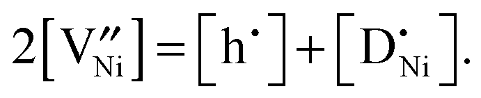 | (5) |
 ] largely exceeds [h˙], the mass action constant is
 | (6) |
 will be the major Ni-defect within a much greater temperature and pO2 range, e.g., see ref. 24.
The defect concentrations (here in terms of molar fractions) for undoped and donor-doped NiO were calculated by using mass action constants from the literature25 for a small dopant concentration of 10−4. The calculations show that the vacancy concentration  is around 2.5 × 10⁻⁶ for undoped NiO, while it is 2.5 × 10⁻⁴ for donor-doped NiO at 600 °C at 0.21 bar O2.23 The results of the calculations demonstrate that even a small amount of dopant influences the defect concentrations by several orders of magnitude, and the influence increases at low temperatures. This information indicates the possibility to enhance cation diffusion by increasing the Ni vacancy concentration, thereby enhancing the oxidation rate constant.
1.2. Oxidation kinetics of metals
For the growth of a crack-free, adhering oxide layer on a metal film, the metal has to diffuse outwards and/or oxygen inwards, comprising transport of ionic and electronic carriers. If the molar volumes of the growing oxide layer and the metal do not differ extremely, the growing oxide layer is expected to be compact.26,27 Depending on the actual conditions, the oxidation kinetics is described by different models (see e.g., ref. 3): (i) the Cabrera–Mott theory2 describes the formation of very thin oxide films at relatively low temperatures, at which the electric field resulting from tunneling of electrons from the metal to chemisorbed oxygen species at the oxide surface accelerates ionic transport across the film. The decrease of the electric field with increasing film thickness leads to a negligible growth rate once a “limiting thickness” of a few nanometers is reached. Since under the conditions used in the present work the oxidation kinetics does not follow the Cabrera–Mott theory, it is not discussed in detail. (ii) In the second case characterized by negligible field effects (relevant for thick films at high temperature), the kinetics is controlled either by chemical diffusion through the oxide layer as described by the Wagner theory or by surface reactions.The Wagner theory considers the diffusion controlled formation of a compact oxide layer.1,27–29 The oxidation process is determined by the ambipolar conductivity (σδ = σeonσion/(σeon + σion)) together with the chemical potential gradient through the oxide film (see Fig. 1b). Depending on the defect chemistry and the electronic structure of the oxide, metal or oxygen ions can dominate ion diffusion, and the electronic current is carried by electrons or holes. For NiO, metal ions and holes are the major diffusing species. The flux of metal ions is directly related to the increase of the oxide thickness X and is given by
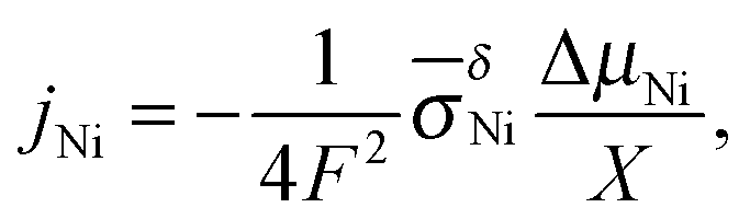 | (7) |
| X2 = kpt | (8) |
 . In general, the parabolic rate constant kp is related to the tracer diffusion coefficient D* by
 | (9) |
 is the diffusivity of Ni ions in NiO and NA is the Avogadro number. Since teon is close to 1 for NiO, eqn (9) results in
 | (10) |
 | (11) |
 is the molar Gibbs energy of oxide formation and
  is the respective standard value, while
  is the standard pressure of 1 bar and pO2 is the actual oxygen partial pressure. For Ni vacancies,
  is given by
 | (12) |
 is the diffusivity of
  , and
, and  is the concentration in terms of site fraction.
  is weakly dependent on pO2 because
  ∝ pO21/2 (see eqn (3)).
 | ||
| Fig. 1 The profiles of the chemical potentials (μNi and μO) for (a) surface reaction controlled oxidation and (b) chemical-diffusion controlled oxidation (in practice the change of μO and μNi within the oxide film is not perfectly linear). | ||
If the reaction is surface controlled, the oxygen and defect concentrations are homogeneous through the growing oxide film and there is a chemical potential step at the surface, corresponding to a deviation in oxygen concentration (δcO) from the equilibrium value (Fig. 1a). The flux of ions is given by
| jO = −jNi = −kδδcO, | (13) |
 is the effective surface reaction rate constant. δcO remains constant as long as some metal remains beneath the oxide film. As a consequence, eqn (13) yields a constant flux of ions corresponding to a constant oxide thickness growth rate.
2. Experimental methods
Polycrystalline Ni films were prepared in a thickness range of 10–150 nm by e-beam evaporation at ∼10−6 Torr from Ni (99.5%, Alfa Aesar) at room temperature on polycrystalline (KERAFOL, 0.25 mm thick) and single crystalline Al2O3 (sapphire, CrysTec, 0.25 mm thick) substrates. The thicknesses of the films were measured with a surface profilometer (Dektak XT, Bruker). Platinum electrodes (∼400 nm) were sputter-deposited (Edwards Auto 306 at 5 × 10⁻² mbar Ar, 60 W) using a shadow mask.The 0.1 and 1 at% Cr-doped Ni alloys have been prepared by alloying the required amounts of Cr and Ni metals (for details see ref. 23). Chemical analysis by inductively coupled plasma optical emission spectroscopy (ICP-OES) yielded concentrations of 0.138 ± 0.002% Cr for nominally 0.1% Cr-doped Ni, and 1.03 ± 0.02% Cr for nominally 1% Cr-doped Ni. From these alloys thin films were grown by e-beam evaporation (under the same conditions as used for Ni films) and by scanning femto-pulsed laser deposition (femto-PLD). Using PLD, approximately 100 nm thick Cr-doped Ni films were deposited on sapphire substrates at a substrate temperature of −180 °C for 2 hours using a femtosecond laser (442 fs, femtoRegenIC-375, High-Q-Laser GmbH, 516 nm, 30–50 mW, 1 kHz). An alloyed target disc (1% Cr-doped Ni, Ø = 10 mm) was rotated (1.4 rpm) at a fixed angle in a vacuum chamber (3 × 10⁻⁸ mbar) and ablated by a horizontal line scan (galvanometer mirror box, HurryScan25, Scanlab AG, 50 mm s−1) of the laser beam focused on the target surface (spot size of 0.04 mm, for further details on the method see ref. 30). The substrate temperature was controlled using a Pt-100 temperature sensor placed in the sample holder and fixed at −180 °C during deposition.
DC magnetron sputtering (ATC 1500-F Sputtering System, Aja International Inc.) was used for the deposition of 100 nm thick 1% Cr-doped Ni films. The films were grown by using simultaneous sputtering of Ni and Cr targets at 250 W and 3 W, respectively.23
During the oxidation of the films in air in a tube furnace, the resistance changes were measured laterally across the samples by two-point electrical impedance spectroscopy (Newton PSM1700 and Novocontrol Alpha-A High Performance Frequency Analyzer, 100 Hz to 1 MHz at 100 mV AC amplitude) and fitted with an equivalent circuit modeling software (ZView, Scribner Associates, Inc.). The oxide thickness was calculated from the resistance values of the remaining metallic part of the film, considering the molar volume difference between the metal and the oxide.
Additional measurements under modified experimental conditions, such as UV light exposure, different oxygen partial pressures, and ozone atmosphere, were performed to further investigate the oxidation kinetics of Ni. More experimental details are given in ref. 23.
X-ray photoelectron spectroscopy (XPS), AXIS ULTRA from Kratos Analytical Ltd, was used to determine Cr dopant concentration depth profiles of the metallic and oxide films by Ar ion sputtering (4 kV). The peak positions were compared with the NIST XPS database. According to XPS, the native oxide layer on Ni films has a typical thickness below 3 nm.
Scanning electron microscopy (SEM) was used to determine the grain size of the metal and the oxide films with a Zeiss Merlin microscope in secondary electron detection mode. Transmission electron microscopy (TEM), Philips CM 200, was applied to investigate the microstructure of the films. TEM samples were prepared by focused ion beam (FIB) while observing the process using a scanning electron microscope (Zeiss Crossbeam 1540 ESB).
3. Results and discussion
3.1. Oxidation kinetics of nickel films
Fig. 2a shows the increase of oxide layer thickness with time in a log–log plot as an exemplary of in situ thin film oxidation measurements. The slope is close to 1/2, indicating a parabolic rate law (diffusion controlled oxidation). If the reaction was surface controlled, the oxide film thickness would grow linearly in time (slope = 1). For the film thicknesses between 10 and 150 nm, the slope of 1/2 indicated in Fig. 2b confirms the diffusion controlled oxidation. Furthermore, the parabolic rate constant for films of different thicknesses and different substrates (polycrystalline Al2O3 or sapphire) yields essentially the same value (Fig. 3a). | ||
Fig. 2 (a) Logarithmic scaling of the measured oxide thickness X as a function of time for oxidation of the 50 nm Ni film at 360 °C and (b) slope of log X vs. log![[thin space (1/6-em)]](https://www.rsc.org/images/entities/char_2009.gif) t as a function of the measured film thickness. t as a function of the measured film thickness. | ||
 | ||
| Fig. 3 Measured oxidation rate constants (a) for different Ni film thicknesses on polycrystalline Al2O3 or sapphire substrates in air and (b) for 50 nm Ni films on polycrystalline Al2O3 substrates under different experimental conditions. | ||
Ni films were oxidized with different pO2, ozone atmosphere, and UV light exposure (Fig. 3b). These experiments confirmed that in a temperature range of 250–500 °C, the oxidation kinetics of Ni is diffusion controlled for films of 10–150 nm thicknesses. This conclusion is drawn because the different experimental conditions, which are expected to strongly accelerate (UV, O3) or decelerate (low pO2) the surface reaction, did not significantly change the overall oxidation rate constant.
The fact that the oxidation of thin Ni films is diffusion controlled is attributed to the comparably small  values of NiO. In general, the rate determining process is expected to change from diffusion controlled to surface reaction controlled below a certain critical thickness which is given by lc ≈ D*/k* (k*: surface reaction rate, lc: critical sample thickness, D*: tracer diffusion coefficient).31 The value of lc ranges typically from 1 to 100 μm for mixed conducting perovskites.31 Although the smallest sample thickness in the present work equaled only 10 nm, a change from diffusion control to surface reaction control was not observed. Also upper limits of k* values were calculated in the present study for 10 nm NiO films using
  values. These values are comparable to k* of redox-active mixed conducting perovskites,32 while the tracer diffusivity in NiO is much lower than the tracer diffusivity in perovskites.33,34 We therefore conclude that lc in NiO is smaller by orders of magnitude than in perovskites.
The temperature range studied in the present work was 250 to 500 °C, whereas the literature studies were mainly performed in a temperature range between 500 and 1400 °C.10–16 Selected literature results11–13,35,36 and the results of this work are shown in Fig. 4. The scatter of the literature kp values reflects the influence of several factors on the oxidation of Ni: the nature and concentration of impurities, the grain size of the growing oxide,3 preparation techniques of the metal (annealed and cold worked),37 and crystal orientation.38 The oxidation of Ni films in the present work reveals faster oxidation compared to the reported data in the literature.11–13,35,36
 | ||
Fig. 4 Parabolic rate constants for Ni oxidation as reported in ref. 11–13, 35 and 36 compared to the results of this work. Open symbols were calculated from eqn (10) using  values of single crystalline NiO from ref. 13. Since the pO2 range of different data sets is small (0.2 to 1 bar O2) and the pO2 dependence of kp is weak, these data sets are comparable. values of single crystalline NiO from ref. 13. Since the pO2 range of different data sets is small (0.2 to 1 bar O2) and the pO2 dependence of kp is weak, these data sets are comparable. | ||
The vast majority of polycrystalline samples have a higher oxidation rate constant than the kp values calculated from single crystalline  values, and a lower activation energy as shown in Fig. 4. This result indicates that the grain boundaries provide fast diffusion paths as indicated in the literature.3,39 The activation energy in Atkinson and Taylor's work is given as 2.6 eV for bulk diffusion, 2.0 eV for dislocation diffusion and 1.8 eV for grain boundary diffusion of Ni in NiO.39 Although the values of the activation energies differ in the literature, the present results (Ea of
  calculated from kp of 1.7 ± 0.1 eV) are in good agreement with the published values, especially with the results reported by Atkinson and Taylor.39 The kp values of the present work are two orders of magnitude higher than for the large-grained polycrystalline samples reported in ref. 11, which is ascribed to the small grain sizes of the samples in the present work. The grain sizes of a partly oxidized 100 nm thick Ni film were investigated by SEM and TEM, as shown in Fig. 5. The lateral grain size of the metallic layer is ∼100 nm, whereas the grain sizes of the oxide layer vary between 10 and 30 nm. The pore formation between Ni and NiO shown in Fig. 5 was attributed to faster grain boundary diffusion of Ni in NiO compared to Ni in Ni.40
 | ||
| Fig. 5 Cross-sectional (a) SEM and (b) TEM images of the partly oxidized 100 nm Ni film. | ||
The effective diffusion coefficient can be modeled assuming a parallel switching of bulk transport and fast grain boundary diffusion according to
 | (14) |
 is the effective diffusion coefficient,
  the grain boundary diffusion coefficient, and
  the grain (bulk) diffusion coefficient. The thickness of the grain boundary (δ) is assumed to be 1 nm while the average grain size (d) is 20 nm as measured by TEM for the samples in this work. The volume fraction of the grain boundaries g is calculated to be equal to 0.1 according to g = qδ/d and by using q = 2 for the thin films (columnar grains; q = 1 would correspond to the microstructure of vertical lamellae41).
Fig. 6 shows that in NiO the grain boundary diffusion coefficient below 700 °C exceeds the bulk diffusion coefficient by more than five orders of magnitude. Fig. 6 furthermore shows that  is close to
  , revealing that grain boundaries control the diffusion of Ni in the present thin NiO films. Using the calculated
  for a ceramic sample which has a 0.16 μm grain size yields
  at 560 °C, which is in reasonable agreement with a measured diffusion coefficient of 1.8 × 10⁻¹⁴ cm2 s−1 at 560 °C, as in ref. 11. We therefore conclude that the accelerated grain boundary transport properties of the NiO thin films are quite similar to those of the oxide-ceramic samples.
 | ||
Fig. 6 Comparison of the calculated grain boundary diffusion coefficients ( : squares) derived using eqn (14), the effective diffusion coefficient derived using eqn (10) from measured kp values in this work ( : squares) derived using eqn (14), the effective diffusion coefficient derived using eqn (10) from measured kp values in this work ( : triangles), and the bulk diffusion coefficient ( : triangles), and the bulk diffusion coefficient ( : circles) from ref. 13. : circles) from ref. 13. | ||
3.2. Oxidation kinetics of Cr-doped Ni films
 | ||
| Fig. 7 Measured oxidation rate constants of Ni films: undoped (50 nm on the polycrystalline substrate), 1% Cr-doped (50 nm on the polycrystalline Al2O3 substrate), and 0.1% Cr-doped (50 nm and 12 nm on the sapphire substrate). | ||
To understand the reason for the Cr dopant inactivity, we performed XPS and TEM studies on the Cr-doped Ni films.
The measured concentration depth profiles of 0.1 and 1% Cr-doped Ni samples before and after oxidation analyzed by XPS with Ar ion sputtering are given in Fig. 8. The XPS depth profiles revealed an enhanced amount of Cr on the metallic sample surface. Cr2O3 has a significantly more negative standard free energy of formation than NiO, therefore Cr accumulates in the native oxide layer.
 | ||
| Fig. 8 Concentration depth profile analysis by XPS of (a) the 0.1% Cr-doped Ni metal film, (b) the 0.1% Cr-doped Ni oxidized film, (c) the 1% Cr-doped Ni metal film, and (d) the 1% Cr-doped Ni oxidized film. The raise of the Al signal at long sputtering times indicates the sputtering process reaching the Al2O3 substrate. | ||
After oxidation of the films, most Cr is found as a segregated layer at the bottom of the film. Obviously, the outward diffusion of Cr through the growing oxide layer is slower than Ni diffusion, which is also observed in the literature.49–51 Since the Cr dopant is evidently strongly depleted in most of the growing oxide layer, it is understandable that the Cr-doped Ni films showed similar oxidation rate constants to undoped Ni films.
TEM studies illustrate the morphology of fully oxidized Cr-doped Ni films for 0.1 and 1% Cr. While the bottom layer is not easily visible in Fig. 9a for 0.1% Cr, the presence of a bottom layer corresponding to the Cr-enriched zone is clear for 1% Cr films (Fig. 9b).
 | ||
| Fig. 9 Cross-sectional TEM images of (a) 0.1% Cr-doped NiO and (b) 1% Cr-doped NiO films grown on the polycrystalline Al2O3 substrates. | ||
4. Conclusions
The rate determining process for the oxidation of 10–150 nm thick Ni films at 250–500 °C is found to be diffusion of nickel via nickel vacancies through the oxide layer. The process is well described by the Wagner theory. The oxidation is diffusion controlled even for the thinnest films (10 nm) because the cation tracer diffusion coefficient in most common binary oxides is comparably low (in contrast to the oxygen tracer diffusion coefficient in perovskites). The increased oxidation rate constants and therefore the effective diffusion coefficients for the present samples with a much smaller oxide grain size compared to the literature show the importance of fast grain boundary diffusion. While donor doping is expected to increase the parabolic rate constant of Ni films, our measurements of e-beam evaporated and magnetron sputter deposited Cr-doped films show no change in the oxidation rate constant because of severe Cr segregation to the interface between the NiO film and the substrate.Acknowledgements
The authors gratefully acknowledge the technical support and valuable discussions provided by Yvonne Stuhlhofer, Helga Hoier, Mitsuharu Konuma, Bernard Fenk, Fritz Phillipp, Marion Kelsch, Reinhart Völker, Gerhard Werner, Matej Fonovic, and Iman Rastegar.References
- C. Wagner, Z. Phys. Chem., Abt. B, 1933, 21, 25–41 Search PubMed.
- N. Cabrera and N. Mott, Rep. Prog. Phys., 1949, 12, 163–184 CAS.
- A. Atkinson, Rev. Mod. Phys., 1985, 57, 437–470 CrossRef CAS.
- N. Halem, M. Abrudeanu and G. Petot-Ervas, J. Mater. Sci. Eng. B, 2011, 176, 1002–1009 CrossRef CAS.
- M. Tsuchiya, S. K. R. S. Sankaranarayanan and S. Ramanathan, Prog. Mater. Sci., 2009, 54, 981–1057 Search PubMed.
- W. W. Smeltzer and D. J. Young, Prog. Solid State Chem., 1975, 10, 17–54 CrossRef.
- R. Haugsrud, J. Mater. Sci. Eng. A, 2001, 298, 216–226 CrossRef.
- K. R. Lawless, Rep. Prog. Phys., 1974, 37, 231 CrossRef CAS.
- A. Galerie, High Temperature Corrosion of Chromia-forming Iron, Nickel and Cobalt-base Alloys in Shreir's Corrosion, Elsevier Ltd, Amsterdam, 2010 Search PubMed.
- A. Hughes, A. Atkinson and A. Chadwick, MRS Online Proc. Libr., 1984, 24, 27–37 CrossRef CAS.
- A. Atkinson, R. Taylor and A. Hughes, Philos. Mag. A, 1982, 45, 823–833 CrossRef CAS.
- S. Mrowec and Z. Grzesik, J. Phys. Chem. Solids, 2004, 65, 1651–1657 CrossRef CAS.
- A. Atkinson and R. I. Taylor, J. Mater. Sci., 1978, 13, 427–432 Search PubMed.
- S. Song and P. Xiao, J. Mater. Sci. Eng. A, 2002, 323, 27–31 CrossRef.
- S. Mrowec, Z. Grzesik, B. Rajchel, A. Gil and J. Dabek, J. Phys. Chem. Solids, 2005, 66, 115–120 CrossRef CAS.
- S. Mrowec and K. Przybylski, Oxid. Met., 1985, 23, 107–139 CrossRef CAS.
- M. Graham and M. Cohen, J. Electrochem. Soc., 1972, 119, 879–882 CrossRef CAS.
- F. P. Fehlner, J. Electrochem. Soc., 1984, 131, 1645 CrossRef CAS.
- Y. Unutulmazsoy, R. Merkle, I. Rastegar, J. Maier and J. Mannhart, APL Mater., 2017, 5, 042302 CrossRef.
- P. Kofstad, Nonstoichiometry, Diffusion, Electrical Conductivity in Binary Metal Oxides, Wiley-Interscience, New York, 1972 Search PubMed.
- F. Kröger and H. Vink, Solid State Phys., 1956, 3, 307–435 Search PubMed . In this notation, the type of defect is represented by a major symbol (e.g., V: vacancy), the site is indicated by a subscript (e.g., Oo or VNi) and the relative charge of defect is indicated by a superscript (negative charge: ′ and positive charge: ˙).
 represents an oxygen ion on its regular lattice site,
  is a nickel vacancy on a nickel site which is doubly ionized.
 - R. Farhi and G. Petot-Ervas, J. Phys. Chem. Solids, 1978, 39, 1175–1179 CrossRef CAS.
- Y. Unutulmazsoy, PhD Thesis, University of Stuttgart, 2016.
- H. Meier and R. Rapp, Z. Phys. Chem., 1971, 54, 168–189 CrossRef.
- G. Koel and P. Gellings, Oxid. Met., 1972, 5, 185–203 CrossRef CAS.
- R. E. Bedworth and N. B. Pilling, J. Inst. Met., 1923, 29, 529–582 Search PubMed.
- H. Schmalzried, Chemical Kinetics of Solids, John Wiley & Sons, 2008 Search PubMed.
- J. Maier, Physical Chemistry of Ionic Materials: Ions and Electrons in Solids, John Wiley & Sons, 2004 Search PubMed.
- H. Schmalzried, Solid State Reactions, Vch Pub., 1981 Search PubMed.
- D. Fischer, G. de La Fuente and M. Jansen, Rev. Sci. Instrum., 2012, 83, 043901 CrossRef CAS PubMed.
- H. J. M. Bouwmeester, H. Kruidhof and A. J. Burggraaf, Solid State Ionics, 1994, 72, 185–194 CrossRef CAS.
- L. Wang, R. Merkle, J. Maier, T. Acartürk and U. Starke, Appl. Phys. Lett., 2009, 94, 071908 CrossRef.
- J. Claus, M. Leonhardt and J. Maier, J. Phys. Chem. Solids, 2000, 61, 1199–1207 CrossRef CAS.
- R. A. De Souza and J. A. Kilner, Solid State Ionics, 1998, 106, 175–187 CrossRef CAS.
- O. Kubaschewski and B. E. Hopkins, Oxidation of Metals and Alloys, Butterworths, 1967 Search PubMed.
- K. Fueki and J. B. Wagner, J. Electrochem. Soc., 1965, 112, 384–388 CrossRef CAS.
- D. Caplan, M. Graham and M. Cohen, J. Electrochem. Soc., 1972, 119, 1205–1215 CrossRef CAS.
- N. Khoi, W. Smeltzer and J. Embury, J. Electrochem. Soc., 1975, 122, 1495–1503 CrossRef CAS.
- A. Atkinson and R. Taylor, Philos. Mag. A, 1981, 43, 979–998 CrossRef CAS.
- R. Nakamura, J.-G. Lee, H. Mori and H. Nakajima, Philos. Mag., 2008, 88, 257–264 CrossRef CAS.
- H. Mehrer, Diffusion in Solids: Fundamentals, Methods, Materials, Diffusion-Controlled Processes, Springer Science & Business Media, 2007 Search PubMed.
- F. Stott and G. Wood, Corros. Sci., 1977, 17, 647–670 CrossRef CAS.
- G. Petot-Ervas and C. Petot, J. Phys. Chem. Solids, 1990, 51, 901–906 CrossRef.
- H. Atkinson, Oxid. Met., 1985, 24, 177–197 CrossRef CAS.
- A. Atkinson and D. W. Smart, J. Electrochem. Soc., 1988, 135, 2886–2893 CrossRef CAS.
- A. Atkinson, D. Smart and R. Taylor, Mater. Corros., 1987, 38, 704–709 CrossRef CAS.
- C. H. Chen, M. R. Notis and D. B. Williams, J. Am. Ceram. Soc., 1983, 66, 566–571 CrossRef CAS.
- S. Mrowec, J. Nowotny, T. Walec and T. Wojcikiewicz, Bull. Acad. Pol. Sci., Ser. Sci. Chim., 1973, 21, 829–837 CAS.
- W. Chen, N. Peterson and L. Robinson, J. Phys. Chem. Solids, 1973, 34, 705–709 CrossRef CAS.
- M. Seltzer, J. Electrochem. Soc., 1971, 118, 802–805 CrossRef CAS.
- A. Atkinson and R. Taylor, J. Phys. Chem. Solids, 1986, 47, 315–323 CrossRef CAS.


| This journal is © the Owner Societies 2017 |