
 Open Access Article
 This Open Access Article is licensed under a Creative Commons Attribution-Non Commercial 3.0 Unported Licence
The real structure of ε-Ga2O3 and its relation to κ-phase
Ildikó
Cora
 *a,
Francesco
Mezzadri
b,
Francesco
Boschi
cd,
Matteo
Bosi
d,
Maria
Čaplovičová
e,
Gianluca
Calestani
bd,
István
Dódony
f,
Béla
Pécz
a and
Roberto
Fornari
cd
*a,
Francesco
Mezzadri
b,
Francesco
Boschi
cd,
Matteo
Bosi
d,
Maria
Čaplovičová
e,
Gianluca
Calestani
bd,
István
Dódony
f,
Béla
Pécz
a and
Roberto
Fornari
cd
aCentre for Energy Research, Hungarian Academy of Sciences, Institute for Technical Physics and Materials Science, P.O. Box 49, H-1525 Budapest, Hungary. E-mail: coraildiko@gmail.com
bDepartment of Chemistry, Life Sciences and Environmental Sustainability, University of Parma, Parco Area delle Scienze 17/A, 43124 Parma, Italy
cDepartment of Mathematical, Physical and Computer Sciences, University of Parma, Parco Area delle Scienze 7/A, 43124 Parma, Italy
dIMEM-CNR, Parco Area delle Scienze 37/A, 43124 Parma, Italy
eSlovak University of Technology, University Science Park Bratislava Centre, Vazova 5, 812 43, Bratislava, Slovak Republik
fDepartment of Mineralogy, Eötvös Loránd University, Pázmány P. stny. 1/C, Budapest, Hungary
First published on 17th February 2017
Abstract
A comprehensive study by high-resolution transmission electron microscopy (TEM) and X-ray diffraction (XRD) was carried out on Ga2O3 epilayers grown at low temperature (650 °C) by vapor phase epitaxy in order to investigate the real structure at the nanoscale. Initial XRD measurements showed that the films were of the so-called ε phase; i.e. they exhibited hexagonal P63mc space group symmetry, characterized by disordered and partial occupation of the Ga sites. This work clarifies the crystal structure of Ga2O3 layers deposited at low temperature at the nanoscale: TEM investigation demonstrates that the Ga atoms and vacancies are not randomly distributed, but actually possess ordering, with (110)-twinned domains of 5–10 nm size. Each domain has orthorhombic structure with Pna21 space group symmetry, referred to as κ-Ga2O3. Further XRD analysis carried out on thicker samples (9–10 μm) confirmed this finding and provided refined structural parameters. The six (110)-type twinned ordered domains together – if the domain size falls below the actual resolution of the probing techniques – can be misinterpreted as the disordered structure with its P63mc space group symmetry usually referred to as ε-Ga2O3 in the current literature. The crystal structure of these Ga2O3 layers consists of an ABAC oxygen close-packed stacking, where Ga atoms occupy octahedral and tetrahedral sites in between, forming two types of polyhedral layers parallel to (001). The edge-sharing octahedra and the corner-sharing tetrahedra form zig-zag ribbons along the [100] direction. Anti-phase boundaries are common inside the domains. The polar character of the structure is confirmed, in agreement with the characteristics of the Pna21 space group and previous observations.
1. Introduction
Ga2O3 is a binary oxide of great interest for its advantageous physical properties and demonstrated applications in electronics, opto-electronics, UV-detection, catalysis, etc.1 Polymorphism is a major issue in the case of gallium oxide, and unfortunately it is still poorly understood. Four different polymorphs were described in the ICSD database: α,2 β,3–5 γ,6–8 ε;9 amongst these polymorphs β-Ga2O3 is the only thermodynamically stable phase and for this reason it is the most extensively studied. All mentioned structures are composed by a similar close-packed arrangement of oxygen atoms, in which gallium octahedral and tetrahedral sites are occupied in different ratios. The proportion of tetrahedrally and octahedrally coordinated Ga is 1![[thin space (1/6-em)]](https://www.rsc.org/images/entities/char_2009.gif) :1 in the monoclinic β-phase. Thanks to its large bandgap (4.7–4.9 eV) and large electric breakdown field (8 MV cm−1) this phase is particularly suitable for high power devices.1 α-Ga2O3 has a corundum structure3 containing only octahedrally coordinated Ga and is metastable,10 in contrast to its alumina analogue and converts to β-Ga2O3 over 650 °C. The γ-phase has a spinel-type structure11 and is also metastable. ε and δ-phases were first prepared and examined by Roy et al. in 1952.6 They studied these phases by X-ray powder diffraction, making use of tabulated d-spacings and relative intensity values. Moreover, the reaction scheme that they used resulted in the interconversions of polymorphs. A full structural characterization was however hindered by the poor quality of the crystalline aggregates obtained via chemical routes, which were further unavoidably contaminated by the β phase. In a recent reappraisal of Roy's work, Playford et al. reported a total neutron diffraction investigation of these polymorphs.12
:1 in the monoclinic β-phase. Thanks to its large bandgap (4.7–4.9 eV) and large electric breakdown field (8 MV cm−1) this phase is particularly suitable for high power devices.1 α-Ga2O3 has a corundum structure3 containing only octahedrally coordinated Ga and is metastable,10 in contrast to its alumina analogue and converts to β-Ga2O3 over 650 °C. The γ-phase has a spinel-type structure11 and is also metastable. ε and δ-phases were first prepared and examined by Roy et al. in 1952.6 They studied these phases by X-ray powder diffraction, making use of tabulated d-spacings and relative intensity values. Moreover, the reaction scheme that they used resulted in the interconversions of polymorphs. A full structural characterization was however hindered by the poor quality of the crystalline aggregates obtained via chemical routes, which were further unavoidably contaminated by the β phase. In a recent reappraisal of Roy's work, Playford et al. reported a total neutron diffraction investigation of these polymorphs.12
According to first principle calculations,9,13 the ε-phase is the second most stable polymorph after β. In the last years the growth of single-phase ε-Ga2O3 thin films was demonstrated on commercial sapphire as well as other hexagonal or pseudo-hexagonal substrates.14–16 It was also shown that epitaxial ε-Ga2O3 is relatively stable and that converts to β only after prolonged annealing at T > 700–800 °C.14,16 This allows sufficiently high working temperatures, at least for some categories of devices such as solar blind photodetectors. Considering that its bandgap (about 4.9 eV (ref. 14)) is comparable to the one of β phase, the ε polymorph is of great interest for technological applications, as well as from a fundamental point of view.
ε-Ga2O3 was assigned to the hexagonal P63mc space group, consisting of a 4H stacking of close-packed oxygen layers, in which the disordered Ga atoms occupy octahedral and tetrahedral sites to give the 2:3 (8:12) stoichiometry.12,14,16,17 A transient polymorph κ was also identified by Playford et al.,12 showing the same orthorhombic structure as κ-Al2O3, but authors claimed it was not possible to isolate it from the β-oxide. A possible ordering scheme of the Ga in the hexagonal ε-Ga2O3 (edge-sharing octahedral and corner sharing tetrahedral and octahedra forming zig-zag ribbons) results in the orthorhombic κ-Ga2O3 as an ordered subgroup of the hexagonal ε-Ga2O3 phase. None of these polymorphs were examined at the nanoscale using transmission electron microscope (TEM) techniques and a possible ordering scheme in the ε-phase has not been revealed so far.
In this paper, we describe the real structure of Ga2O3 films deposited by MOVPE (metal–organic vapour phase epitaxy) at low temperature on α-Al2O3, using high-resolution transmission electron microscopy and X-ray diffraction techniques. Ga2O3 grown under the very same conditions were examined recently by Mezzadri et al.17 using XRD. They determined the structure to be P63mc in which Ga atoms occupy octa- and tetrahedral sites which are occupied randomly with a 66% probability and detected a clear ferroelectric behaviour of this ε polymorph. However, no conclusions could be drawn about the way of ordering of the Ga atoms in the structure.
The disordering of the Ga atoms in the epsilon phase was only determined by XRD and never examined before by TEM, therefore nano-scale ordering of this phase was not studied yet. In this work we intend to assess the real structure of this phase and reveal the structural relationship between ε- and κ-phase. The parallel X-ray diffraction (XRD) analysis, carried out on very thick samples (10 μm), also permitted to assess the order–disorder phenomena in an independent way.
2. Experimental section
The epitaxial growth of Ga2O3 layers was performed by using a MOVPE reactor in a stainless steel chamber. The epilayers were deposited on (001) α-Al2O3 substrates at 650 °C using trimethylgallium (TMG) and ultrapure water as reagents, while ultrapure H2 was employed as carrier gas. Two different samples were specifically prepared for this work: a thin one, about 250 nm, was used for TEM investigations while a thicker one, about 10 μm was used for XRD More details about the growth process are reported in ref. 15.Cross-sectional and plan-view samples for TEM analysis were prepared by Ar ion beam milling. Preparation details of the present samples were given elsewhere.18 Charging of the sample was significant therefore a few nm thin amorphous carbon layer was evaporated to reduce it. The thinned samples were examined using a Philips CM20 transmission electron microscope operating at 200 kV, and bright-field (BF) images and selected area electron diffraction (SAED) patterns were taken onto imaging plate detector. HRTEM images, SAED patterns were acquired using a JEOL 3010 operating at 300 kV with LaB6 cathode onto a Gatan Orius CCD camera. The scanning transmission electron microscope (STEM) images were taken in a JEOL JEM ARM200cF (double Cs corrected, 200 kV, cFEG cathode).
A sample suitable for single crystal diffraction experiments was obtained by mechanically removing a 100 × 100 × 10 μm3 fragment of the thicker Ga2O3 from the sapphire substrate. Single crystal diffraction data were collected by using a Bruker APEX II diffractometer equipped with a CCD area-detector and graphite monochromatized MoKα radiation. Structure solution and refinement were carried out using the Sir2011,19 and Shelxl20 programs, respectively. Further information on the crystal structure investigation may be obtained from FIZ Karlsruhe, 76344 Eggenstein-Leopoldshafen, Germany (fax: (+49)7247 808 666; e-mail: E-mail: crysdata@fiz-karlsruhe.de) on quoting the deposition number CSD-432326.
3. Transmission electron microscopy
3.1 Crystal structure of the Ga2O3 film
The bright field (BF) TEM image of Ga2O3 film on the α-Al2O3 substrate is shown in (Fig. 1). The 250 nm thick Ga2O3 layer has a columnar structure revealed by amplitude and phase contrast, presenting columns with diameter of about 2–10 nm. At the substrate interface a different phase is observed: the fast Fourier-transform (FFT) of this very thin region (10–50 nm), shown on HRTEM image also reported in (Fig. 1) indicates that this phase can be indexed as γ-Ga2O3.6 Both of these phases were grown epitaxially onto the α-Al2O3 substrate (Fig. 1). | ||
| Fig. 1 BF image, SAED pattern and HRTEM image with the corresponding indexed FFTs (A and B) of the epitaxial Ga2O3 thin film on α-Al2O3 surface in cross section. At the interface another phase could be identified as γ-Ga2O3 (region and FFT signed B). The upper (main part of this study) Ga-oxide phase shows a columnar texture. The reflections could be indexed in an orthorhombic unit cell (region and FFT marked). | ||
The occurrence of the γ-phase at the interface is an unexpected result, and its presence was evident only after specific TEM investigations. Although the role of the γ-phase may be important for the actual growth mechanism of Ga2O3 on α-Al2O3 at the used temperature, its origin and evolution are still unclear and we plan a more thorough investigation in order to understand when and how the γ-phase nucleates and its relationship with the growth process parameters. The present work will be essentially devoted to the detailed study of the columnar Ga2O3 phase dominant in all examined samples.
We examined the thinned plan-view section of the film as well. On the HRTEM images (Fig. 2A) we clearly observed the domain structure (cross section of the columns), with domains of 2–10 nm diameter. The selected area electron diffraction (SAED) pattern in [001] projection shows a hexagonal symmetry (Fig. 3B). Although, we used the smallest aperture for area selection (200 nm and 50 nm in diameter), several columns/domains were involved in the scattering. In Fig. 2 the fast Fourier transforms (FFTs) of the individual domains selected in the HRTEM image have the same orthorhombic symmetry. These are (110)-twinned domains, related to each other by 120° rotation, thus resulting in a pseudo-hexagonal symmetry of the SAED pattern. FFT of a larger area of the HRTEM image shows a similar metric and intensity distribution as the SAED pattern (Fig. 3A and B).
 | ||
| Fig. 2 HRTEM image (A) of the plan-view section of the sample in [001] projection with the corresponding FFTs (B–E) (FFTs are from 5 nm × 5 nm large area). Each domain shows orthorhombic symmetry (B–D) and rotated to each other by 120°. FFT of the whole image (F) shows a pseudo-hexagonal symmetry. | ||
 | ||
| Fig. 3 Experimental FFT (A) of HRTEM image shown on Fig. 2A, experimental SAED pattern (B) and simulated diffraction pattern (C) along [001] direction for 10 nm sample thickness applying dynamical approximation for JEOL3010 microscope using JEMS software23 package. They show similar intensity distribution. And in [100] projection experimental SAED image (D) and simulated diffraction pattern (E) for 15 nm sample thickness applying dynamical approximation for JEOL3010 microscope using JEMS software23 package. | ||
Based on SAED patterns (Fig. 1 and 3B) we found an orthorhombic unit cell with parameters a0 = 5.0 Å, b0 = 8.68 Å, c0 = 9.23 Å. On the thinnest part of the prepared section we could identify the systematic absences: from h00, 0k0 and 00l reflections → h,k,l = 2n, from 0kl reflections → k + l = 2n. Along the ![[a with combining low line]](https://www.rsc.org/images/entities/b_char_0061_0332.gif) * and
* and ![[b with combining low line]](https://www.rsc.org/images/entities/b_char_0062_0332.gif) * directions some diffuse streaks are observed suggesting the presence of defects corresponding to these directions.
* directions some diffuse streaks are observed suggesting the presence of defects corresponding to these directions.
A raw HAADF image, its Fourier-filtered, and the symmetry averaged images of the cross-sectioned sample can be seen in Fig. 4. Layered structure of the Ga2O3 was obvious in the cross-section (Fig. 5). The found 2D symmetry is: cm (m is ⊥ to ). Line scans of the layers for highlighting the intensity distribution can be seen in Fig. 5B and C. The bright spots in the image correspond to the Ga atom-columns. Although the images were taken from the thin part of the sample, it is worth mentioning that we see overlapping of more columns/domains on STEM image, since the specimen thickness (at least 15–20 nm) was surely larger than the domain thickness.
 | ||
| Fig. 4 A) Experimental STEM HAADF images in [100] projection (cross section of the film) of the columnar Ga2O3. B) Fourier-filtered experimental image. C) Symmetry averaged image using Crisp software package.21 The right part of the STEM HAADF image was used for further processing. The found/recovered 2D symmetry is: cm (m is ⊥ to ). | ||
 | ||
| Fig. 5 Fourier-filtered, symmetry averaged STEM HAADF image of the columnar Ga2O3 in [100] projection (the cross section of the film, A), and the corresponding line-scans (B and C) calculated by Digital Micrograph. Bright peaks/densities correspond to the positions of the Ga-atom columns. We note that on the STEM image we see the overlapping of more columns/domains, since the specimen thickness was larger than the domain thickness. | ||
Two types of polyhedral layers were identified: in the line scan in Fig. 5C we see two atomic columns closer to the top and two atomic columns closer to the bottom.
Based on the data presented above, we concluded that in this phase the Ga is ordered (i.e. its sof value is equal to 1) and the structure shows a domain-structure at the nano-scale. The crystal structure of each Ga2O3 domain is analogous to the kappa-alumina (κ-Al2O3).22Fig. 6 shows the polyhedral representation of this structure. Oxygen can be described as an ABAC close-packed stacking and Ga3+ atoms occupy octahedra and tetrahedra forming two types of polyhedral layers parallel to (001): pure octahedral layer and a mixed, octa- and tetrahedral layer. The edge-sharing octahedra and the corner-sharing tetrahedra form zig-zag ribbons along the [100] direction. This acentric structure has the same unit cell as κ-Al2O3 and Pna21 space group is conform with the extinction rules that we found in the studied Ga2O3 and the 2D symmetry (cm where m is ⊥ to ) revealed from STEM HAADF image. This structural configuration results in the 2:3 Ga:O ratio.
 | ||
| Fig. 6 The κ-Ga2O3 structure in [100] (A) and [001] (B) projections. In the octahedral layers the octahedra (yellow) forms ribbons parallel to [100] (C), as well as the tetrahedra and the octahedra in the mixed layer (red). | ||
Characteristic of the sample is the abundant twinning resulting in domain structure: the growth direction of the ribbons change their orientation by 120°, i.e. the hexagonal stacking of the O layers is preserved, but the Ga-centered octahedra chains follow another pseudo-hexagonal <100> direction. The above findings are confirmed by plan view HRTEM images.
We calculated the diffraction patterns for the [100] (cross-section) and [001] (plan-view) projections of 15 and 10 nm sample thicknesses, applying dynamical approximation (Fig. 3) using the JEMS software package.23 Intensity distribution of the experimental SAED and calculated pattern are pretty similar apart from the very weak diffuse scattering.
In STEM HAADF images the brightness maxima show the Ga positions. In the Fig. 4 and 5 the [100] projected Ga2O3 shows extra intensities in the octahedral layer between the successive octahedral ribbons (i.e. the four Ga-columns). On the other hand, the four Ga-columns do not have the same intensity and the two middle peaks out of the four have higher intensity. In the thicker part of the sample the intensity distribution of this Ga peaks in the pure octahedral layer is equalized. The reason for the intensity variation is that the result of the overlapping of these (110) twinned domains in cross section. Actually, if the sample is thick enough, we can see only an averaged structure.
3.2 Twin and anti-phase boundaries revealed by TEM
In [001] projected HRTEM images numerous defects/boundaries can be identified. These defects are also evident in cross section (HRTEM images of [100] projection). Two main types can be distinguished: twin-boundaries (TB) and anti-phase boundaries (APB) (Fig. 7).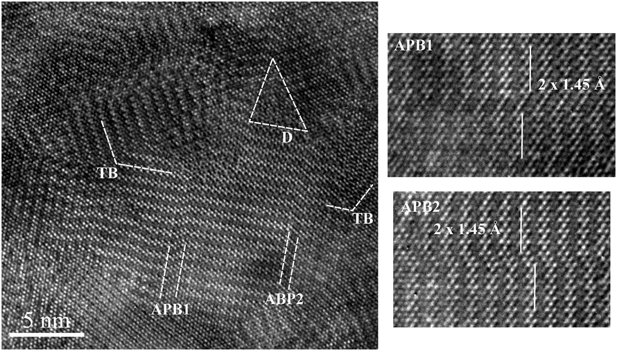 | ||
| Fig. 7 [001] projected HRTEM image of the plan-view section of the sample showing the cross sections of the columns/domains. Numerous defects/boundaries can be identified from which two main types are: twin-boundaries (TB) and anti-phase boundaries (AP). Disordered regions (D) are also observed at the boundary of the twin domains. Two magnified images can be seen on the right about antiphase boundaries. 2 elementary shifts combined that results 2 × 1.45 Å large shift of the structure. | ||
Twin boundaries can be well understood in this structure. While the ABAC close-packed stacking of the oxygen atoms remain the same, the positions of the Ga atoms are twinned. Fig. 8A shows the polyhedral model representation of the (110) twin boundary.
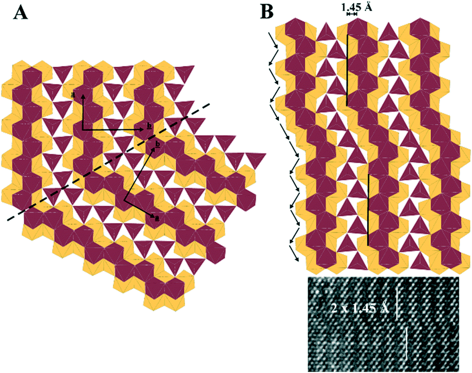 | ||
| Fig. 8 A) Polyhedral structural model of the (110) twin boundary. B) Polyhedral structural model of anti-phase boundary inside the domains. 2 elementary shifts combined resulting in 2 × 1.45 Å large shift of the structure. | ||
We found parts in cross section with disturbed contrast along the boundaries between domains. This feature is probably due to overlapping of the twin domains growing along the c direction. Also poorly ordered regions, i.e. where Ga atoms are not well ordered, might be another reason for the disturbed contrast.
Isolated anti-phase boundaries occur inside the twin domains (Fig. 7) parallel to (100). Anti-phase shift in the structure can be clearly seen from the HRTEM images, ![[R with combining low line]](https://www.rsc.org/images/entities/b_char_0052_0332.gif) = −1/6 ; || = 1.45 Å, which can be easily interpreted as the shift of the octahedra stacking in the b direction along the growing of the ribbons. This shift (anti-phase boundary) can be repeated resulting in a thicker multi defect zone, therefore the extent of the shift will be the multiplication of 1.45 Å. Fig. 8B presents the structural model of a multi anti-phase boundary/zone. The largest shift zone was 2.9 Å wide. Hypothetically, if the formation of this shift is thermodynamically favorable and the shift zone is large enough, a new polymorph can form as a new ordered subgroup of the ε-phase.
= −1/6 ; || = 1.45 Å, which can be easily interpreted as the shift of the octahedra stacking in the b direction along the growing of the ribbons. This shift (anti-phase boundary) can be repeated resulting in a thicker multi defect zone, therefore the extent of the shift will be the multiplication of 1.45 Å. Fig. 8B presents the structural model of a multi anti-phase boundary/zone. The largest shift zone was 2.9 Å wide. Hypothetically, if the formation of this shift is thermodynamically favorable and the shift zone is large enough, a new polymorph can form as a new ordered subgroup of the ε-phase.
4. XRD characterization
The preparation of a thicker sample, showing an average larger size of the ordered domains, allowed to extend previous investigations17 performed by single crystal XRD. This analysis allowed to fully validate them, providing in addition a quantitative structural information which is mandatory for an effective modelling of the system as well as for the understanding of its macroscopic properties. The performed collection of the complete Ewald-sphere using a CCD area detector was elaborated by using the Precession Images plugin of the Bruker APEX2 software. The reconstructed precession image of the hk0 projection is shown in Fig. 9. This XRD pattern, showing an apparent 6mm symmetry, agrees with the SAED reported in Fig. 3B. The diffraction spots are characterized, as in the whole diffraction figure, by streaking features that represent the typical fingerprint of domains, spatially limited along an equivalent direction, rotated by 120° around the projection axis and separated by (110) twin boundaries. Therefore, in agreement with the TEM characterization, the XRD pattern can be considered to be the superimposition of the diffraction contributions generated by three orthorhombic lattices, rotated by 120° with respect to each other, according to the (110) twin law:
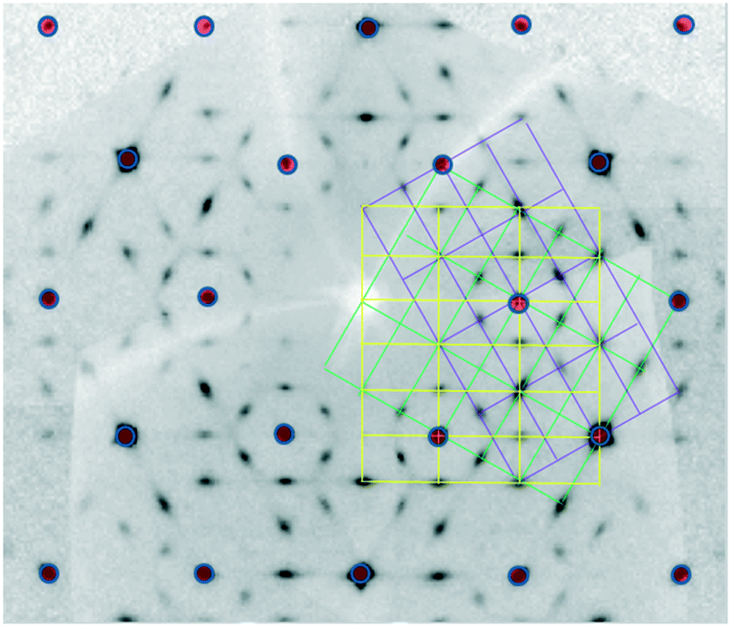 | ||
| Fig. 9 Reconstructed hk0 precession image of κ-Ga2O3 showing the superimposition of the three lattices related to the possible orthorhombic twin variants. The red spots correspond to the reflections of the hexagonal fundamental disordered lattice with lattice parameters a = 2.9081(7) Å and c = 9.262(3) Å. | ||
A suitable indexing of the diffraction pattern, allowed for a refinement of the lattice parameters, which were estimated to be: a = 5.0463(15), b = 8.7020(9), c = 9.2833(16) Å. As the κ-Ga2O3 structure is non-centrosymmetric, the integration of the diffraction intensities required the use of 6 twin variants, three of them corresponding to the identified rotation domains and three additional ones, metrically coincident to the previous, related to the inversion of the polar axis.
Due to the partial superposition of the reciprocal lattices nodes of the twinning domains, shown in Fig. 9, the extinction rules cannot be determined unambiguously by the integrated intensities. The space group determination was therefore carried out by using the ISODISTORT software. The orthorhombic structure was considered as a commensurate superstructure generated from the fundamental structure of the ε-Ga2O3 (hexagonal P63mc, a = 2.9081(7), c = 9.262(3) Å), i.e. the disordered one previously determined,17 by the modulation vector ![[q with combining low line]](https://www.rsc.org/images/entities/b_char_0071_0332.gif) = (1/6, 1/6, 0) driving the ordering of Ga-sites occupancy. The interpretation of the diffraction pattern in these terms is shown in Fig. 10.
= (1/6, 1/6, 0) driving the ordering of Ga-sites occupancy. The interpretation of the diffraction pattern in these terms is shown in Fig. 10.
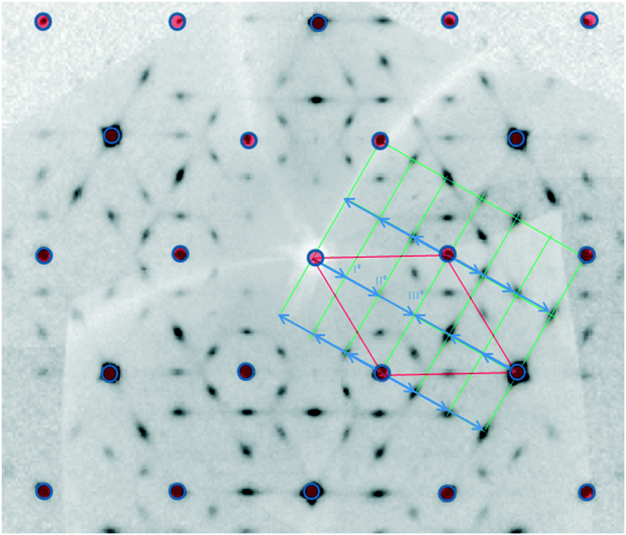 | ||
| Fig. 10 Reconstructed hk0 precession image of κ-Ga2O3. The red spots highlight the fundamental reflections, while the green lattice corresponds to one of the possible twin variants. In blue the 3rd order modulation vector = (1/6 1/6 0) is shown. | ||
The symmetry reduction resulting from the combination of the fundamental P63mc symmetry with the (1/6, 1/6, 0) modulation vector generated a limited number of space groups corresponding to the superstructure lattice: four of these are orthorhombic, Pmc21, Pca21, Pmn21, Pna21, and the remaining one is monoclinic, Pc.
The structure solution was attempted in all the five possible space groups on merged data produced by TWINABS24 but only Pna21, gave good results in terms of both agreement indices and crystal structure reliability.
The structure refinement was then successfully carried out (by using the HKLF5 option of SHELXL20) on the intensity data integrated on the six twin variants. The complexity of the experimental features, limiting in some extent a precise evaluation of the diffraction intensity (in particular the presence of the twin variants, the streaking of the diffraction spots, the quasi-two dimensional character of the sample strongly influencing the absorption correction and the presence of the minor amount of the γ phase) reflected on the refinement, in particular for what concerned the atomic displacement parameters (a.d.p.s). Consequently, those of one gallium atoms and the ones of the oxygen atoms were fixed to reasonable values during the refinements leading to final values of the agreement indices (R1 = 0.0830, gof = 1.11) which, under these conditions, can be considered as satisfactory. No deviation from the complete occupancy of all the independent crystallographic sites was detected in the refinement, yielding the expected 2/3 value for the stoichiometric gallium/oxygen ratio. The details and the results of the structural refinement are summarized in Table 1.
| Crystal data | Refinement parameters | |||||
|---|---|---|---|---|---|---|
| Orthorhombic | Radiation type | Mo Kα | ||||
| a = 5.0463(15) Å | (sinθ/λ)max (Å−1) |
0.600 | ||||
| b = 8.7020(9) Å | μ (mm−1) | 26.10 | ||||
| c = 9.2833(16) Å | Meas./indep./obs.[I > 2σ(I)] refl. | 3285/3285/2627 | ||||
| V = 407.66(15) Å3 | R[F2 > 2σ(F2)], wR(F2), S | 0.083, 0.238, 1.11 | ||||
| D x = 6.108 g cm−3 | Parameters | 40 | ||||
| s.g. Pna21 (n. 33) | Restraints | 1 | ||||
| Atom coordinates | ||||||
|---|---|---|---|---|---|---|
| Ga1 | 4a | 0.1838(9) | 0.3398(4) | 0.0278(5) | 1 | 0.002 |
| Ga2 | 4a | 0.6754(9) | 0.5304(5) | 0.0369(6) | 1 | 0.0049(10) |
| Ga3 | 4a | 0.1891(11) | 0.6527(8) | 0.2503(5) | 1 | 0.0062(12) |
| Ga4 | 4a | 0.1742(11) | 0.6529(9) | −0.1607(6) | 1 | 0.0103(14) |
| O1 | 4a | 0.350(7) | 0.492(3) | 0.137(4) | 1 | 0.005 |
| O2 | 4a | −0.016(9) | 0.494(3) | −0.093(4) | 1 | 0.005 |
| O3 | 4a | 0.335(6) | 0.154(3) | 0.150(4) | 1 | 0.005 |
| O4 | 4a | 0.847(6) | 0.670(4) | 0.169(4) | 1 | 0.005 |
| O5 | 4a | 0.000(9) | 0.829(3) | 0.409(4) | 1 | 0.005 |
| O6 | 4a | 0.508(10) | 0.666(3) | −0.097(4) | 1 | 0.005 |
5. Discussion
The present study deals with epitaxial Ga2O3 with a columnar structure, as evidenced by TEM. Previous XRD studies on a 3 μm thick film grown in the same conditions by some of the authors17 suggested that the film has the ε-structure of hexagonal P63mc space group symmetry with partial occupation of Ga sites and disordered Ga atoms. In the same paper, it was stated that the observed fractional occupation of the different Ga sites could have been either compatible with a merely statistical occupation or with short-range ordered domains. However, it was impossible to discriminate between these two cases as the employed X-ray technique, with its inherent resolution, could just provide a mediated view.The present detailed TEM studies are now able to show that the structure is ordered in 5–10 nm large domains, and each domain has an orthorhombic structure with Pna21 space group symmetry, called κ-Ga2O3. New XRD analysis carried out on a much thicker sample (10 μm) confirmed the results obtained by TEM, and permitted to obtain the refined structural parameters, reported here for the first time, at the best of authors' knowledge.
κ-Gallium oxide was first reported by Playford et al.12 who studied Ga-oxide polymorphism by neutron and X-ray powder diffraction applying Rietveld-refinement. They produced Ga5O7(OH) as a result of solvothermal oxidation reactions. During the thermal decomposition of this oxyhydroxide they found a phase, called κ-gallium oxide, before transformation into β-Ga2O3. They only gave the cell parameters for this structure. This publication is important, as it explicitly showed that one of the reaction products could be a novel metastable phase (in the form of powder).
In κ-Ga2O3 the oxygen positions can be described as a 4H (ABAC) close-packed stacking and Ga3+ atoms occupy octahedra and tetrahedra forming two types of polyhedral layer parallel to (001) (see Fig. 6). The edge-sharing octahedra and the corner-sharing tetrahedra form zig-zag ribbons along the [100] direction, resulting in the orthorhombic Pna21 space group symmetry.
This structure has an analogue among Al-oxide as well, the so-called κ-alumina. The structure is commonly twinned, giving rise to domain/columnar structure, since the growth direction of the ribbons rotated by 120° while the pseudo-hexagonal 4H stacking of the O atoms is preserved. When the domain size falls below the coherence length of the radiation used in the X-ray or neutron diffraction experiments, an apparent hexagonal symmetry is recovered in the diffraction patterns. In other words, when the ordering range is below the actual resolution of the probing techniques, one may uniquely see the averaged, disordered structure with its P63mc space group symmetry usually referred to as ε-Ga2O3 in the current literature.
The orthorhombic κ-Ga2O3 is as an ordered subgroup of the hexagonal ε-Ga2O3 phase, deriving from a peculiar arrangement of Ga atoms between the O planes. It is appropriate to call this orthorhombic phase κ-Ga2O3, considering the analogous Al-oxide phase and the previous nomenclature12 and the possibility for existence of other ordering schemes of Ga atoms which has not been revealed yet. However, these nm sized domains, i.e. the nm scaled ordering can be easily investigated in situ and separately in a TEM.
Although the present findings cannot readily be extended to all published results on the structure of ε-Ga2O3 (e.g.ref. 14–16), we strongly suspect that the definition of ε-Ga2O3 as purely hexagonal polymorph needs to be amended considering the ordered κ structure evidenced in the present work.
The refined average interatomic distance for the tetrahedral site is 1.83(4) Å, while for the octahedral ones it ranges from 2.01(4) to 2.05(4) Å, in good agreement with the tabulated values. The structural analysis clearly points out the polar character of the structure, in agreement with the non-centrosymmetric Pna21 space group. This is revealed by the analysis of the “out of plane” distances of the gallium atoms with respect to the mean oxygen layers, adjacent along the ![[c with combining low line]](https://www.rsc.org/images/entities/b_i_char_0063_0332.gif) axis. As shown on Fig. 11, a positive resultant of the cationic displacements is observed along the positive direction of the axis and generates a net dipole moment in the same direction. The dipole moment, calculated from the refined atomic coordinates, results to be 0.20 μC cm−2 and conforms to the ferroelectric nature of the compound, recently unveiled thanks to the direct measurement of the hysteresis loop.17
axis. As shown on Fig. 11, a positive resultant of the cationic displacements is observed along the positive direction of the axis and generates a net dipole moment in the same direction. The dipole moment, calculated from the refined atomic coordinates, results to be 0.20 μC cm−2 and conforms to the ferroelectric nature of the compound, recently unveiled thanks to the direct measurement of the hysteresis loop.17
 | ||
| Fig. 11 “Out of plane” distances (Å) of the gallium atoms from the mean oxygen layers adjacent along the polar c axis. | ||
6. Conclusions
The real structure of the Ga2O3 layer deposited by MOVPE on an α-Al2O3 substrate at 650 °C was accurately investigated by TEM and XRD. The layers showed a columnar structure perpendicular to the interface, whose origin was correlated with formation of small domains. The Ga2O3 structure can be considered as a 4H (ABAC) close-packed stacking of oxygen atoms along the axis, where Ga atoms occupy octahedral and tetrahedral sites forming two types of polyhedral layers parallel to (001). Detailed TEM studies showed that the structure is ordered in 5–10 nm large domains, and each domain has an orthorhombic structure with Pna21 space group symmetry, called κ-Ga2O3. Anti-phase boundaries were also observed and modeled inside the domains, which could be more extended (several octahedral large) along the [100]. Further investigations are needed to understand the growth mechanism of this ordered phase and to relate domain size and twin boundaries to process parameters.
We provided here the refined atomic parameters (unit cell data, atomic coordinates) for the orthorhombic κ-Ga2O3 and we confirmed the polar character of the structure, in agreement with the characteristics of its Pna21 space group.
If the size of the ordered domains, i.e. the ordering scale, is below the actual resolution of the probing techniques, one may uniquely see the average, i.e. disordered structure, with its P63mc space group symmetry, usually referred to as ε-Ga2O3 in the current literature. However, these nm sized domains, i.e. the nm scaled ordering can be easily investigated in situ and separately in a TEM. It would be interesting to check if the present observations apply to ε-Ga2O3 epilayers of other groups.
Learning the detailed defect structure is the first step to grow homogeneous layers of κ-gallium oxide. Further investigations are needed to understand the growing mechanism of this new ordered phase and to relate domain size and twin boundaries to process parameters.
Acknowledgements
Exchange of samples and researchers' visits were possible in the framework of the bilateral scientific agreement between CNR and MTA. The authors gratefully thank to Noémi Szász for her kind effort in sample preparation.Maria Čaplovičová thanks for the support of the Ministry of Education, Science, Research and Sport of the Slovak Republic within the Research and Development Operational Programme for the project “University Science Park of STU Bratislava”, ITMS 26240220084, co-funded by the European Regional Development Fund.
Notes and references
- M. Higashiwaki, K. Sasaki, H. Murakami, Y. Kumagai, A. Koukitu, A. Kuramata, T. Masui and S. Yamakoshi, Semicond. Sci. Technol., 2016, 31, 34001 CrossRef.
- I. Levin and D. Brandon, J. Am. Ceram. Soc., 2005, 81, 1995–2012 CrossRef.
- S. Geller, J. Chem. Phys., 1960, 33, 676–684 CrossRef CAS.
- S. Geller, J. Solid State Chem., 1977, 20, 209–210 CrossRef CAS.
- J. Åhman, G. Svensson and J. Albertsson, Acta Crystallogr., Sect. C: Cryst. Struct. Commun., 1996, 52, 1336–1338 CrossRef.
- R. Roy, V. G. Hill and E. F. Osborn, J. Am. Chem. Soc., 1952, 74, 719 CrossRef CAS.
- T. N. T. Sato, Thermochim. Acta, 1982, 53, 281–288 CrossRef CAS.
- L. A. O'Dell, S. L. P. Savin, A. V. Chadwick and M. E. Smith, Appl. Magn. Reson., 2007, 32, 527–546 CrossRef.
- S. Yoshioka, H. Hayashi, A. Kuwabara, F. Oba, K. Matsunaga and I. Tanaka, J. Phys.: Condens. Matter, 2007, 19, 346211 CrossRef.
- W. H. Zachariasen, Skrifter utgitt av det Norske Videnskaps-Akademi i Oslo 1: Matematisk-Naturvidenskapelig Klasse, 1928, 4, 6–166 Search PubMed.
- S.-W. Kim, S. Iwamoto and M. Inoue, Ceram. Int., 2009, 35, 1603–1609 CrossRef CAS.
- H. Y. Playford, A. C. Hannon, E. R. Barney and R. I. Walton, Chem. - Eur. J., 2013, 19, 2803–2813 CrossRef CAS PubMed.
- M. B. Maccioni and V. Fiorentini, Appl. Phys. Express, 2016, 9, 41102 CrossRef.
- Y. Oshima, E. G. Víllora, Y. Matsushita, S. Yamamoto and K. Shimamura, J. Appl. Phys., 2015, 118, 85301 CrossRef.
- F. Boschi, M. Bosi, T. Berzina, E. Buffagni, C. Ferrari and R. Fornari, J. Cryst. Growth, 2016, 443, 25–30 CrossRef CAS.
- X. Xia, Y. Chen, Q. Feng, H. Liang, P. Tao, M. Xu and G. Du, Appl. Phys. Lett., 2016, 108, 202103 CrossRef.
- F. Mezzadri, G. Calestani, F. Boschi, D. Delmonte, M. Bosi and R. Fornari, Inorg. Chem., 2016, 55, 12079 CrossRef PubMed.
- A. Barna, G. Radnóczi and B. Pécz, Handbook of Microscopy, in: Handb. Microsc., ed. S. Amelinc, VCH Verlag, 1997, p. 751 Search PubMed.
- M. C. Burla, R. Caliandro, M. Camalli, B. Carrozzini, G. L. Cascarano, C. Giacovazzo, M. Mallamo, A. Mazzone, G. Polidori and R. Spagna, J. Appl. Crystallogr., 2012, 45, 357–361 CrossRef CAS.
- G. M. Sheldrick, Acta Crystallogr., Sect. C: Struct. Chem., 2015, 71, 3–8 CrossRef PubMed.
- S. Hovmöller, Ultramicroscopy, 1992, 41, 121–135 CrossRef.
- B. Ollivier, R. Retoux, P. Lacorre, D. Massiot and G. Férey, J. Mater. Chem., 1997, 7, 1049–1056 RSC.
- P. A. Stadelmann, JEMS, (n.d.), http://www.jems-saas.ch/Home/jemsWebSite/jems.html.
- G. M. Sheldrick, TWINABS, 1996 Search PubMed.
| This journal is © The Royal Society of Chemistry 2017 |