
 Open Access Article
 This Open Access Article is licensed under a Creative Commons Attribution-Non Commercial 3.0 Unported Licence
Hybrid plasmonic–photonic whispering gallery mode resonators for sensing: a critical review
Angelo
Bozzola
 ,
Sara
Perotto
and
Francesco
De Angelis
*
,
Sara
Perotto
and
Francesco
De Angelis
*
Istituto Italiano di Tecnologia, via Morego 30, I-16163, Genova, Italy. E-mail: francesco.deangelis@iit.it
First published on 22nd February 2017
Abstract
In this review we present the state of the art and the most recent advances in the field of optical sensing with hybrid plasmonic–photonic whispering gallery mode (WGM) resonators. After a brief introduction on the basic physics behind photonic WGM resonators and localized surface plasmon (LSP) nanostructures, we analyze the different types of optical sensors specifically designed for bulk refractive index sensing, molecular binding and single object detection. We point out the physical and technological key points of the different approaches proposed in the literature, and we systematically compare hybrid sensors and purely photonic WGM sensors. This comparative analysis points out the real advantages brought by LSP nanostructures, and it identifies the most promising hybrid architectures.
 Angelo Bozzola | Angelo Bozzola received his degree and Ph.D. in Physics from the University of Pavia (Italy) in 2010 and 2014, respectively. Since 2015 he has been a postdoc researcher in the Plasmon Nanotechnologies Unit at the Italian Institute of Technology (IIT), Genoa, Italy. He is specialized in the design and electromagnetic simulation of photonic and plasmonic nanostructures and devices. He is interested in Applied Optics, especially in biosensing, solar energy harvesting, and silicon photonics. |
 Sara Perotto | Sara Perotto received her master's degree in applied physics from Università degli studi di Milano Bicocca, Italy, in 2014. Currently she is pursuing her Ph.D. in Plasmon Nanotechnology Unit at the Italian Institute of Technology in Genoa. |
 Francesco De Angelis | Dr Francesco De Angelis holds a Ph.D. in Physics in the field of materials science. Currently, he is senior researcher at the Italian Institute of Technology in Genoa where he leads the Plasmon Nanotechnology Unit. His main expertise relies on micro and nano-optical devices for biomedical applications. He currently holds an IDEAS-ERC Consolidator grant (Neuro-Plasmonics, grant agreement 616213) whose aim is to combine 3D plasmonic nanostructures with CMOS devices to develop radically new interfaces between electrical/optical devices and neuronal networks. He has published more than 100 papers in peer-reviewed journals; total impact factor >700; H index = 34. |
1. Introduction
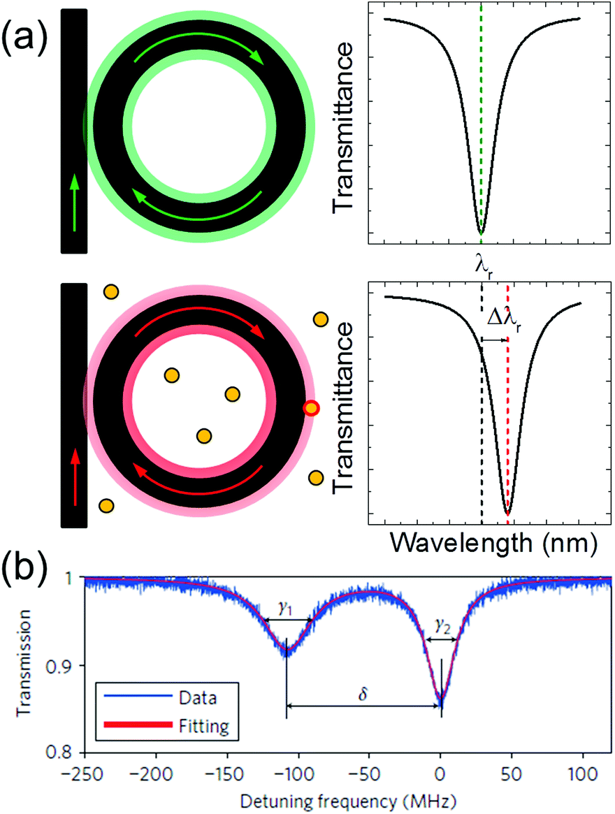
In recent years the field of detection of single particles, viruses, biomarkers, and molecules has been subject to intense study in different scientific communities from medicine to pharmacology, and from nanophysics to chemistry. Purely optical methods are now gaining considerable attention. In particular, optical sensing with whispering gallery mode (WGM) resonators show prospects for the unprecedented sensitivity to very small objects, down to the single molecule level, and a number of technologically relevant drawbacks. These include great stability and robustness in aqueous environments, multiplex operation, scalability, reduced fabrication costs, and the potential for integration in point-of-care and portable devices.The reason behind the high sensitivity of WGM biosensors lies in the fundamental properties of whispering gallery modes. In the optical and infrared domains, WGMs are supported by dielectric microstructures such as spheres, toroids and rings possessing a refractive index larger than the surrounding environment (n approximately equal to 1.33 for water). In these structures light can circulate at the periphery of the resonator, where it is confined by total internal reflection. Briefly, a resonance appears when the length of the optical path of the WGM equals an integer number of wavelengths inside the resonator. Thus, when constructive optical interference occurs, the electromagnetic field exhibits a standing wave profile. At resonance, the mode is mainly confined in the dielectric structure. A portion extends outside the resonator (the so called evanescent tails), and it is sensitive to the external environment. A chemical–physical change, such as the binding of a nanoparticle or a single molecule, perturbs the resonant mode profile and the optical energy distribution inside the resonator. Redshifts of the resonance, broadening, and, in particular circumstances, the splitting of the resonant modes occur. Several excellent reviews already reported on purely photonic WGM sensors.1–8 This field is now differentiating into different subfields, depending on the specific application of interest. Although great efforts have been made to suppress any source of noise in the optical measurement, the detection of single molecules, biomarkers, and proteins with a high signal to noise ratio remains very challenging when using a conventional WGM resonator.
In order to increase the sensitivity to the binding of very small objects, the inclusion of metallic structures was proposed during the last few years. Metallic nanostructures, when properly excited by visible and near-infrared light, can support localized surface plasmon resonances (LSPR). These arise from the collective in-phase oscillations of the free electrons of metals with the incoming electric field. Despite having an intrinsic quality factor much smaller than that of WGM modes, these LSP resonances are characterized by a strong field enhancement and a superior field confinement. The size of these so called hot-spots of electromagnetic energy density can be reduced down to a few nanometres, a value that is well matched to the size of the nano-object of interest. The combination of WGM resonators and plasmonic nanostructures in a new type of hybrid plasmonic–photonic biosensor thus seems particularly promising. The WGM component provides sharp resonances, which are an essential ingredient to monitor the binding of tiny objects (or, in other words, to keep a very low limit of detection). The plasmonic component provides a strong electromagnetic field enhancement, which boosts the sensitivity of the device. The hybrid coupling between photonic and plasmonic modes has already been proposed, for example, between photonic crystal cavities and metallic antennas.9,10 In these studies, the photonic cavity was excited directly from the free space. In the case of hybrid cavities for biosensing, instead, the dielectric cavity is excited from the near field, by means of an optical fibre or with an integrated bus waveguide. This evanescent excitation can be much more efficient and stable compared to free space methods, and it also substantially reduces the background optical noise. From a practical point of view, it is well suited for automated and large-scale on-chip applications which are gaining considerable attention in the field of biosensing.
This review is structured as follows. In section 2 we briefly illustrate the theory behind WGM resonators and in section 3 we focus on metallic LSPR structures for what concerns their application in a hybrid sensing platform. In section 4 we review the state-of-the-art of hybrid biosensors and we perform a systematic comparison between conventional, purely photonic WGM sensors and their hybrid counterparts.
2. WGM resonators
2.1 Basic theory
Optical whispering gallery modes are originated from the total internal reflection of light at an interface (Fig. 1a). From a ray optics point of view, according to the Snell law, when the refractive index of the dielectric resonator exceeds that of the surrounding medium (n1 > n2) and the angle between the wavevector and the normal to the surface exceeds the critical value θc = a![[thin space (1/6-em)]](https://www.rsc.org/images/entities/char_2009.gif) sin(n2/n1), light is confined into the cavity (Fig. 1b). An example of a resonant standing wave profile inside a double resonant sphere system is reported in Fig. 1c.11
sin(n2/n1), light is confined into the cavity (Fig. 1b). An example of a resonant standing wave profile inside a double resonant sphere system is reported in Fig. 1c.11
 | ||
| Fig. 1 (a) Sketch of a light ray travelling inside a spherical dielectric cavity. (b) Illustration of the Snell law: the refractive index of the cavity material is denoted with n1, that of the surrounding medium with n2, and the critical angle for total internal reflection with θc. (c) Optical picture of the standing wave profile in a resonant double sphere cavity system fed by a tapered optical fibre. Reproduced from ref. 11. | ||
From the point of view of wave optics, the field profile inside the WGM resonator and the resonant frequencies can be approximated analytically only for high-symmetry configurations, such as for spherical or cylindrical resonators. The reader interested in these theoretical aspects can find more information in ref. 7, 12 and 13. To a first-order approximation, the spectral positions of the resonances can be written as:
 | (1) |
When the system deviates from a perfect spherical or cylindrical symmetry, analytical treatments cannot be used anymore and numerical approaches are necessary. Readers interested in these computational aspects can find more details in ref. 14–24.
The resonances of WGM cavities are typically monitored through the transmission spectrum of the input fibre/waveguide. Other coupling schemes are possible, such as prism coupling25 and direct free-space coupling.26 In the frequency domain, the transmitted power Pout(ω) is typically Lorentzian:7
 | (2) |
 | ||
| Fig. 2 (a) SEM image of a silicon ring resonator on a silicon-on-insulator (SOI) platform. (b) Corresponding transmittance spectrum: experimental points (symbols) and Lorentzian fit (solid line). Adapted with permission from S. Lin et al., Nano Lett., 2010, 10, 2408–2411 (ref. 27). Copyright 2010 American Chemical Society. | ||
Other quantities are essential to characterize the resonances of WGM resonators. The first is the free spectral range (FSR), i.e. the spectral distance between two consecutive resonances. This depends on the size of the resonator. Large resonators are characterized by a very dense transmission spectrum, small resonators, instead, have widely spaced resonance peaks. The second is the full-width at half-maximum (FWHM), which is determined by the total optical losses in the resonator. The FWHM can be expressed as:
| FWHM = FWHMbend + FWHMabs + FWHMrough, | (3) |
The quality factor (Q) is the most widely used quantity to characterize a WGM resonance, and it is defined as:
 | (4) |
The quality factor is a global quantity depending on the employed materials and geometry, and it is also used to characterize other resonant systems, including metallic nanostructures supporting LSP resonances.
From eqn (1), when the refractive index of the host medium changes due to the presence of an analyte, or when a nano-object attaches to the surface of the resonator, the effective refractive index of the guided mode changes, and this induces a redshift Δλr of the resonant frequency λr. This is the so-called reactive sensing principle, and it is graphically illustrated in Fig. 3a. The resonance shift is typically monitored by sweeping the wavelength of the tunable laser. The radius of the cavity and its quality factor are the most relevant parameters in determining the magnitude of Δλr and the sensing capabilities of an optical biosensor. As it will be illustrated in the next section, larger cavities are typically characterized by a larger Q.
 | ||
| Fig. 3 (a) Graphical illustration of the reactive sensing principle. The resonance of the unperturbed cavity (upper panels) redshifts after the binding of a nanoparticle (bottom panels). (b) Resonance splitting induced by a single nanoparticle bound to a high Q-factor toroidal micro-resonator. Reproduced from ref. 28. | ||
The resonance is sharper – and this is good to detect very small objects – but the redshift can be very small because the nano-object only slightly perturbs the resonant mode. Smaller cavities, on the other hand, have a smaller Q, but Δλr is larger. This has practical advantages because the complexity of the experimental setup needed to monitor the redshift can be substantially reduced. These considerations lead to a trade-off between the detection capabilities and complexity of the experimental setup: the ideal WGM resonator depends on the specific application of interest. It is worth mentioning that the resonance redshift is not the only quantity that can be monitored. In high Q-factor resonators, the resonances can be split or broadened by the presence of a bound nano-object. An example of resonance splitting induced by a polystyrene nanoparticle is illustrated in Fig. 3b. The reader can find more details in ref. 28 and in the recent review by Foreman and co-workers.7
2.2 Geometries, materials and fabrication
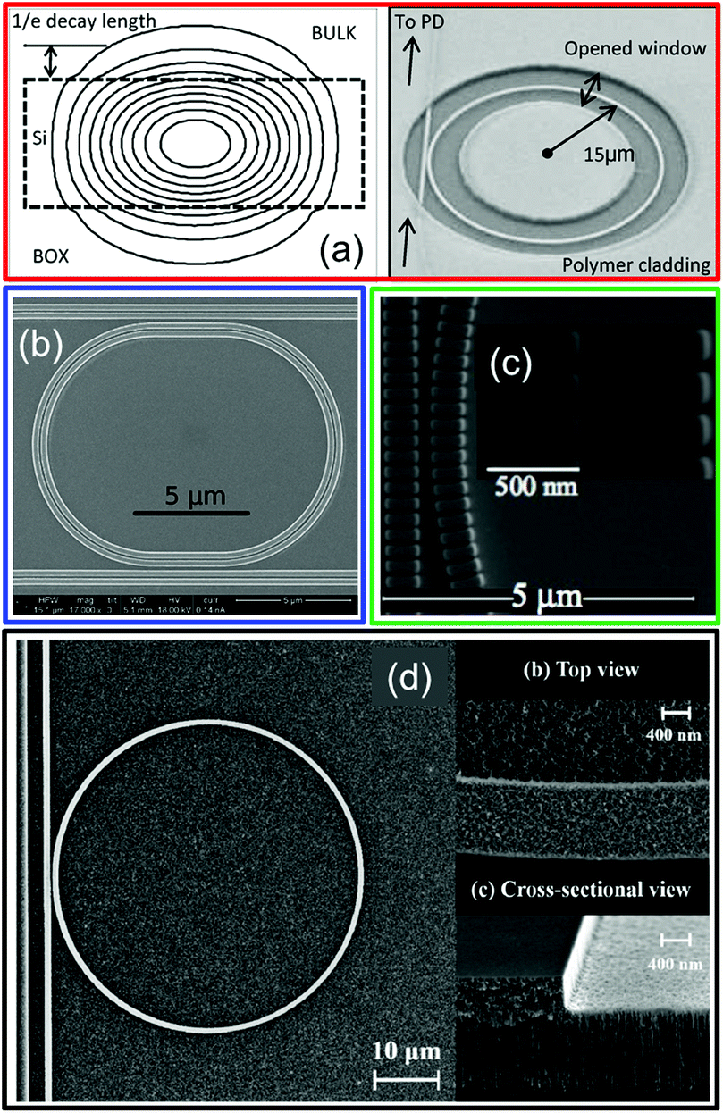
Different dielectric materials have been used to fabricate WGM resonators: fused silica, polymers, silicon and silicon nitride, to cite just a few of them. The choice of a given material depends on the specific geometry and application. Practical examples of cavity geometries are reported in Fig. 4. | ||
| Fig. 4 (a) Optical picture of a glass microsphere resonator attached to an optical fibre. Reproduced from ref. 25. (b) Picture of a capillary resonator. Adapted from ref. 35. (c) SEM image of a fused silica toroidal cavity on a silica substrate. Reproduced from ref. 36. (d) SEM image of a silicon ring resonator on a silicon-on-insulator wafer. Reproduced from ref. 37. | ||
Microsphere resonators (Fig. 4a) are typically made of glass or polymers, and support resonances with very high quality factors up to 108–109 in the visible/near infrared region.3,13,29,30 Such spherical cavities are generally fabricated by heating and stretching the extremity of an optical fibre, and are excited by the same supporting fibre or by another optical fibre brought in close proximity.31,32 Very recently, microsphere resonators have also been immobilized on a glass substrate and light has been coupled via total internal reflection.33,34 These new coupling schemes reduce the complexity of WGM systems, and are useful steps towards the commercialization of optical biosensors. Thanks to their extremely sharp resonances, dielectric microspheres are among the best candidate for single molecule sensing.
Another interesting geometry is the liquid-core optical ring resonator (LCORR – Fig. 4b). In this configuration, the travelling guided mode is confined into the glass or plastic wall of a capillary (total diameters larger than 50–75 μm), and the internal evanescent tail senses the fluid flowing inside.35,38–42 The typical quality factors are in the range 105–107.
Toroidal cavities and disks (Fig. 4c) are fabricated in silicon, glass or polymeric materials and they exhibit high quality factors up to 108.36,43 In silicon and silicon oxide, the fabrication is based on several steps of photolithography, pattern transfer and dry etching, as described, for example, in ref. 36. Also these systems are very good candidates for single object biosensing, as will be illustrated in the next sections. Recent progress in the fabrication methods of all-glass toroids44 on a chip opens new possibilities for the large-scale production of high-Q toroidal cavities for biosensing. As for the case of microsphere resonators, the excitation comes from an optical fibre that is brought in close proximity to the toroid (watch for example the instructive video in ref. 45 for an application of micro-toroids to single particle sensing).
The last category is that of ring and disk resonators on a silicon chip (Fig. 4d). A widely used platform is that of SOI wafers, i.e. silicon wafers where a silicon waveguide layer (hundreds of nm thick) is placed on the top. A silicon oxide buffer layer separates the substrate from the waveguide. Micro-rings and disks can be fabricated with different materials including silicon, silicon nitride, glass or polymers. Typical fabrication techniques are UV lithography,46 electron-beam lithography37 and focused-ion-beam lithography.47 Depending on the ring diameters and materials, the quality factors are in the range 102–106.3,43,48,49 Compared to the other families of WGM resonators, they offer practical advantages. These include the possibility of integrating several devices on a single chip, which is desirable for multiplex operation, and the stable coupling condition, thanks to the waveguide which is directly etched on the platform. In terms of integration with LSPR nanostructures, on-chip microdisks and rings open new prospects compared to the other families of WGM structures. In fact, by adopting dedicated lithographic steps, LSPR structures can be added to the WGM cavity in a controlled way and following a top-down approach. Dielectric ring resonators take advantage of a decade of experience in integrated photonics and electronics. The first commercial biosensors based on ring resonators already appeared on the market,50 and, together with the other families of photonic structures,51–53 they have great potential for future point-of-care applications and portable devices.54
3. Localized surface plasmon resonances in metallic nanostructures
Plasmon resonances in metals arise from the presence of free electrons which can interact with the incident electromagnetic radiation. When electrons are confined into a very small volume, they can oscillate in phase with the incident electric field, thus generating a localized surface plasmon resonance. This is schematically illustrated in Fig. 5, where the electron cloud of a metallic nanosphere is excited by the incoming electric field and oscillates in phase with it. At resonance, the amplitude of the total electric field near the nano-object can be substantially increased compared to the incident amplitude: in this sense we talk about hot-spots confined in close proximity to the LSP structure.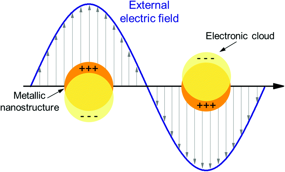 | ||
| Fig. 5 Schematic illustration of a localized surface plasmon (LSP) excited in a small metallic particle. | ||
For the purposes of this review, two important aspects of LSP resonant structures have to be considered. The first is the dependence of the resonant frequency on the refractive index of the surrounding medium. LSP frequencies shift towards the infrared by increasing the refractive index of the environment. This feature is at the basis of bulk refractive index sensing with LSP structures. Excellent reviews on the topic already appeared, and the reader can find all the details in ref. 55–58. Briefly, the bulk sensitivity can reach values up to 1000 nm RIU−1 by properly engineering the aspect ratio of the plasmonic structures (see Fig. 6 and the summarizing work by Khan and co-workers59).
 | ||
| Fig. 6 Bulk sensitivity (in units of nm RIU−1) of different types of plasmonic nanostructures supporting LSP resonances with different aspect ratios. Different symbols correspond to different structures. Reproduced with permission from A. U. Khan et al., J. Phys. Chem. C, 2016, 120, 19353–19364 (ref. 59). Copyright 2016 American Chemical Society. For the meaning of the different colours, lines and shades the reader is referred to ref. 59. | ||
These sensitivity values are enough to track bulk refractive index changes in the range 10−3–10−2 RIU. In recent years nanorods60 and nanorod dimers61 have been employed also for single object sensing, proving, for example, the capability to detect a single protein and track its molecular dynamics in real time, as schematically illustrated in Fig. 7. Although these results are promising, the amplitude of the measured signal is still low compared to the noise introduced during the optical measurement (see Fig. 7c, left panel). As will be illustrated in the next sections, hybrid WGM cavities with plasmonic enhancers have the potential to improve this result, thanks to the tapered-fibre excitation and to the much greater quality factors of hybrid WGM resonances compared to bare LSP resonances.
 | ||
| Fig. 7 Single protein detection using the LSP resonance supported by gold nanorods. (a) Schematic of the experimental opto-fluidic setup used for the time-resolved redshift measurement, (b) time-dependent redshift spectrum monitoring the single binding dynamics, (c) time-dependent redshift spectrum highlighting consecutive binding events, the noise associated with the measurement, and the reference baseline. Adapted with permission from I. Ament et al., Nano Lett., 2012, 12, 1092–1095 (ref. 60). Copyright 2012 American Chemical Society. | ||
The second aspect is evident from Fig. 6: structures with a larger aspect ratio are more sensitive to variations of the external environment. However, when these are integrated onto a dielectric WGM cavity, special care must be paid in order to match the orientation of these elongated structures with the polarization of the circulating electric field. Anisotropic structures possess a strong, intrinsic polarization dependence (consider a nanorod, for example). Care must be taken in order to align the LSP structure with the polarization direction of the WGM field, otherwise resonance broadening or frequency mismatch can have a negative impact on the measurement (see for example the discussion in Fig. 2, ref. 25). This problem does not affect highly symmetric structures such as nanospheres and nanoshells, and this is the reason why these spherical nanostructures were the first to be employed in hybrid WGM cavities for biosensing.
4. Analysis of hybrid WGM resonators
In this section we review the most recent work in the literature where metallic nanostructures are incorporated in photonic WGM resonators in order to improve the sensitivity and the limit of detection. The section is divided into two subsections. In section 4.1 we focus on the structures designed for bulk refractive index sensing and surface binding sensing.These structures are typically fabricated on a chip (in a silicon or silicon nitride architecture), and they include compact nano-sensors whose spectral response redshifts when the refractive index of the liquid environment changes due to the presence of a given analyte of interest. In section 4.2, instead, we focus on hybrid WGM structures for single particle and molecule detection. In this case, the systems are quite different both from the point of view of the resonant structures and excitation conditions. In both the cases we perform a systematic comparison with the state of the art, i.e. with conventional, purely photonic WGM structures not incorporating any LSP nanostructure. The aim of this comparison is to check if the inclusion of the plasmonic component truly brings some advantages compared to the purely photonic WGM sensor in terms of sensitivity and detection limits. Possible future developments are also discussed.
4.1 Hybrid WGM ring and disks for bulk refractive index and surface sensing in a fluid
Purely dielectric micro-rings and disks have been proposed and widely investigated as nano-sensors during the last decade.1,62–80 These systems are very good candidates for the integration on a compact chip. Here several rings can work in parallel in a multiplex architecture. The first test to check the device sensitivity is bulk refractive index sensing.1,62,66,68–70,72,73,76,77,79–81 The device is immersed in a liquid solution of water and glucose,70 sodium chloride,62,68,70 or ethanol70 with different concentrations, which increases the average refractive index of the liquid in a controlled manner. These are important preliminary tests in view of the integration in commercial devices. By monitoring the resonance redshift, it is possible to extract the device sensitivity, which is typically in the range 50–200 nm RIU−1.A more advanced test is the measurement of the concentration of molecules in a solution, or the molecule binding kinetics on the surface of the resonator. In these cases the surface of the ring has to be properly functionalized.1,62,63,65,66,68,69,71,74–77,80 Two examples of bulk refractive index sensing (with a solution of water and sodium chloride) and surface binding (with the biotin/streptavidin complex) are reported in Fig. 8. While physisorption is the route followed for proof-of-concept purposes, covalent attachment of the capturing agent is needed for more complex assays. In order to foster the selective binding to a specific receptor and to avoid nonspecific binding on the inert area of the resonator, the functionalization is carried out by using microfluidics based on PDMS, or specific Mylar gaskets,64 or by spatially directed capturing agent immobilization such as inkjet printing and hand-spotting.82 These approaches improve the sensitivity, reduce the costs, and allow for multiplexed biosensing. The best materials for these devices are silicon and silicon nitride, the latter being suitable also for operation in the visible range of the spectrum. The typical configuration comprises a ring resonator on a chip, which is excited via evanescent coupling from a strip waveguide (Fig. 2a and 4d). Light from a tunable laser or a laser diode is typically coupled into the waveguide from a grating coupler (vertical coupling)83–85 or from the edge of the chip (butt coupling).86,87
 | ||
| Fig. 8 Bulk refractive index sensing. (a) Resonance wavelength shift for a silicon ring resonator immersed in a solution of water and sodium chloride. The experimental points are reported with black squares, the linear fit (sensitivity of 163 nm RIU−1) is reported with a solid line, and the wavelength noise is reported with stars. The experimental limit of detection is 10−6 RIU. (b) Initial binding slope for a functionalized silicon ring resonator immersed in a solution of BSA molecules. The experimental limit of detection is 60 fM, and the dynamic range extends up to 1 μM. Reproduced from ref. 68. | ||
In this simplest ring architecture, only the evanescent tails of the resonant mode can interact with the fluid (Fig. 9a). In this way, light is tightly confined into the waveguide, which leads to a high Q-factor, but the interaction with the analyte in solution – and hence the sensitivity – are quite modest (below 200 nm RIU−1).
 | ||
| Fig. 9 How to make the guided light accessible to the analyte: purely dielectric WGM approaches. (a) Power distribution for the fundamental TE mode in a SOI waveguide (left panel) and fabricated micro-ring resonator for bulk refractive index sensing (right panel). Only the active area is directly exposed to the liquid and functionalized, while the rest is embedded in a protective polymeric cladding. Reproduced from ref. 68. (b) SEM top view of a SOI racetrack micro-ring resonator with a slot waveguide architecture. A 210 nm wide slot width is etched in the middle of the ring. Reproduced from ref. 66. (c) SEM top view of the gap region of a SOI micro-ring resonator based on a sub-wavelength grating waveguide. Reproduced from ref. 78. (d) SEM top view of a micro-ring resonator made of porous silicon (left panel – full device) and zoom of the ring surface and corresponding cross section (right panels). Reproduced from ref. 76. | ||
In order to improve this scenario, the guided optical mode must be more accessible for the analyte in solution. Without including metallic nanostructures, this is possible, for example, adopting a dielectric slot waveguide architecture (Fig. 9b),66 by opening apertures along the circumference of the ring (Fig. 9c),78,79 or by fabricating the ring directly in a porous dielectric medium (Fig. 9d),76 which allows for a direct penetration of the molecules inside the ring. Overall, by using these purely dielectric micro-ring structures, it is possible to detect variations of the refractive index down to 10−7–10−6 RIU, or, equivalently, molecular concentrations down to a few tens of fM.1,68
Another option to make the guided mode more accessible to the analyte is the inclusion of LSP nanostructures. In fact, plasmonic modes are intrinsically “interface” modes, with large evanescent tails extending out of the metal.
This is the main reason why LSPR nanostructures can reach sensitivities up to 1000 nm RIU−1 for bulk refractive index sensing (Fig. 6), which is almost one order of magnitude larger than the corresponding values for photonic microrings and microdisks. During the last decade, two main categories of structures have been proposed: dielectric rings with metallic nanodisks or nanostripes located along the circumference (Fig. 10a),81,88–92 and rings (or disks) in a hybrid metal–dielectric slot configuration (Fig. 10b).93–95 In these latter configurations, the dielectric WGM resonator and the metal layers are separated by a narrow gap, which facilitates the accumulation of optical energy in the aperture accessible to the liquid (inset of Fig. 10b).
 | ||
| Fig. 10 Hybrid WGM structures for bulk refractive index sensing. (a) SOI ring resonator decorated with metallic nanodisks along the circumference. Reproduced from ref. 89 with permission from The Royal Society of Chemistry. (b) Metal–dielectric double slot SOI ring resonator. The inset shows the gap between the silicon ring and the surrounding silver plate, which is the region of accumulation of the electromagnetic field. Reproduced from ref. 94. | ||
When analysing these novel structures and comparing them with the state of the art, the limit of detection (LOD) for bulk refractive index sensing is the main parameter of interest. This quantity is also directly correlated with the lower limit to the number of molecules that can be detected after binding on the surface of the sensor.
The LOD of a WGM structure depends on both the sensitivity (S) and the full-width at half-maximum (FWHM) of the WGM mode. As described in section 2.1, an increase in the refractive index of the surrounding medium causes a redshift Δλr of the resonance. In order to be effectively discriminated from the background noise, Δλr has to be large enough. It is commonly accepted that shifts of the order of 1/1000–1/100 of the FWHM can be detected with an adequate signal-to-noise ratio.60,66,93,96 For this review, we assume Δλr = 1/100 × FWHM as the minimum detectable shift. By extracting the values of S and FWHM from the articles in the literature, it is then possible to compare the sensors directly in terms of LOD:
 | (5) |
We also analyse the LOD for different purely dielectric ring resonators for bulk sensing. We assume the experimental data reported in ref. 62 and 68 as the benchmark for comparison. The results are summarized in Table 1 for a selection of the most relevant work on the hybrid WGM structure for bulk sensing.
| Paper | Type of WGM structure | Theoretical/experimental | Radius (μm) | Operation wavelength (nm) | Quality factor | FWHM (nm) | Sensitivity (nm RIU−1) | Limit of detection (RIU) (eqn (5)) | |
|---|---|---|---|---|---|---|---|---|---|
| 1 | Kwon et al., Sci. Rep., 2016, 6, 23149 | SOI disk + planar Cu slot layer | T + E | 0.9 | 1560 | 24.6 | 63.4 | 214 | 2.96 × 10⁻³ |
| 2 | Urbonas et al., Opt. Lett., 2015, 40, 2977 | SOI ring + Au nanodisks | T | 4 | 1577 | 300 | 5.26 | 176 | 3 × 10⁻⁴ |
| 3 | Ahmed et al., RSC Adv., 2016, 6, 56127 | SOI ring + Fe nanodisks | T | 3.2 | 1950 | 112 | 17.4 | 550 | 3.16 × 10⁻⁴ |
| 4 | Zhang et al., Appl. Opt., 2015, 54, 7131 | SOI ring + Ag ring stripe on the top | T | 5 | 1550 | 80 | 19.4 | 497 | 3.9 × 10⁻⁴ |
| 5 | Zhou et al., Sensors, 2011, 11, 6856 | SOI ring + concentric slot Au disk | T | 1 | 1550 | 85 | 18.24 | 300 | 6.08×10⁻⁴ |
| 6 | Sun et al., Photonics, 2015, 2, 1116 | SOI ring + double planar Ag slot layer | T + E | 6 | 1550 | 300 | 5.16 | 687.5 | 7.5×10⁻⁵ |
| 7 | Chamanzar et al., Appl. Phys. B, 2010, 101, 263 | SiN ring + Ag layer + Al2O3 layer | T | 7.2 | 625 | 1000 | 0.625 | 100 | 6.25 × 10⁻⁵ |
| 8 | Zangeneh-Nejad et al., IEEE Sens. J., 2016, 16, 4338 | SiN ring + graphene layer on top + Al2O3 | T | 7.48 | 150000 |
520 | 288 | 48000 |
6 × 10⁻⁵ |
| 9 | Zhang et al., Opt. Commun., 2016, 380, 6 | Si disk + vertical Ag slot ring | T | 5 | 1550 | 3062 | 0.506 | 100 | 5.06 × 10⁻⁵ |
| 10 | De Vos et al., Opt. Express, 2007, 15, 7610 | Purely photonic racetrack SOI ring | T + E | 5 | 1550 | 20000 |
0.0775 | 70 | 1.1 × 10⁻⁵ |
| 11 | Iqbal et al., IEEE J. Sel. Topics Quantum Electron., 2010, 16, 654 | Purely photonic SOI ring | T + E | 15 | 1550 | 43000 |
0.036 | 163 | 2.21 × 10⁻⁶ |
Compared to the conventional SOI or SiN ring, most of the papers on hybrid structures have just reported theoretical analysis (FEM or FDTD simulations), and only a couple of them (ref. 94 and 95) showed the fabrication and characterization of the devices. All the investigated articles reported on structures operating in the telecom band (λ = 1550 nm), except ref. 90 and 91, which reported on resonators working in the visible (λ = 625 nm) and in the terahertz region (λ = 150 μm, for a novel hybrid device incorporating a graphene layer on the top of a SiN ring resonator). Excluding ref. 91, the maximum reported values for the sensitivity in the VIS-NIR are around 700 nm RIU−1 (both theoretical and experimental). The maximum theoretical Q-factors, instead, are around 3 × 10³, while the experimental Q-factors degrade to less than 300 in fabricated nano-sensors. As a global result, the LOD values calculated according to eqn (5) are consistently above 5 × 10⁻⁵ RIU.
At the moment, the comparison with purely photonic WGM sensors is not favourable. Although the sensitivity of the hybrid WGM resonator is higher than that of a dielectric WGM sensor, the experimental quality factors of purely dielectric microrings are consistently above 104, which is much higher than in the hybrid counterparts. Thus, adopting eqn (5), the experimental LOD is in the range 10−6–10−5 RIU, which is around one order of magnitude lower than the best values for hybrid WGM sensors. Some of the proposed hybrid sensors have a very small footprint (radius smaller than 1 μm),95 which gives a potential advantage in terms of dense packaging on a chip. However, very compact SOI ring resonators (radius of just 1.5 μm) have also been reported, with experimental Q-factors approaching 104 (in air).97
Two relevant aspects emerge from the analysis of the data in Table 1. First, among the hybrid WGM structures, the dielectric–metallic slot ring resonator is probably the best reported structure. The high experimental S values are due to the field accumulation in the gap region (see Fig. 1c in ref. 94). Second, most importantly, it appears that at the moment the Q-factor values are too low for a hybrid refractive index sensor to compete with the pure dielectric counterpart. Considering that for sensors operating near λ = 1.55 μm the maximum enhancement in the sensitivity is 4 after including the metallic nanostructures, and that this is also the maximum tolerable decrease in the Q-factors, it emerges that hybrid plasmonic resonators should possess an experimental Q-factor of 5000–10000 in order to match their purely photonic rivals.
Is it possible to close this gap? For sure such a distance in terms of quality factors is also due to the fact that this field is still in an embryonic stage. The inclusion of a metallic nanostructure in close proximity to a dielectric WGM resonator introduces more defects, such as surface roughness and metal contamination. At the moment, SOI and SiN micro-ring resonators take advantage of decades of experience in the field of micro-electronics and silicon photonics. Many years of fabrication-oriented efforts will be necessary to bring the performance of WGM resonators close to their limits. In addition, for the moment, only very simple LSPR structures have been combined with WGM resonators (disks, stripes and metallic layers in a vertical or horizontal slot configuration). It could be worth investigating more sophisticated plasmonic nanostructures, such as antennas,98,99 dimers,100 or bow-ties101 that take advantage of stronger plasmonic hot-spots and have the potential to reach higher Q-factors.
Other improvements are possible for what concerns the plasmonic materials. The inclusion of gold and silver poses serious problems due to the intrinsic absorption in the metals. Alternative plasmonic materials with lower losses in the visible and near-infrared have been recently proposed, such as transparent doped oxides102–104 and nanocrystals.105 It could be interesting to investigate such novel materials in combination with a dielectric WGM sensor.
4.2 Hybrid WGM structures for single particle and molecule detection
The detection of single objects is the main reason behind the introduction of LSP nanostructures into WGM resonators. In this type of measurement one looks at the resonance shift (or broadening, or splitting) when a single nano-object binds on the surface of the resonator. By looking at the temporal evolution of the binding curve, it is also possible to extract information on the molecular dynamics on the surface of the resonator. From the reactive sensing principle applied to the case of a single particle or molecule,106–110 the resonance redshift Δλr can be expressed in terms of the particle polarizability α and of the value of the electric field at the particle location (E0(rp)):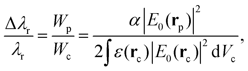 | (6) |
 , Wc is the analogous energy stored in the WGM cavity
  , and ε is the permittivity of the WGM resonator material. For a conventional WGM cavity with no plasmonic enhancement, E0(rp) is simply the value of the evanescent tail of field at the surface of the resonator. When a plasmonic structure is attached to the cavity surface, this value can be substantially increased (up to a factor of a few thousands106,111,112) thanks to the localized plasmon resonance. The typical dimensions of these hot-spots are also comparable to the dimensions of the target particles/molecules, which makes plasmonic nanostructures particularly interesting for single nano-object detection. Concerning the single particle detection, the LOD for the particle size is not a well-defined quantity because it depends on the refractive index of the particle and on the surface functionalization, that is the homogeneity of the capturing agent layer and its affinity to the analyte.113
Purely dielectric WGM resonators have been investigated in detail over the last decade.2,7,11,28,29,96,114–121 The most influential papers on WGM single particle detection are analyzed in Table 2, where we report the principal parameters of the involved structures and their detection capabilities.
| Paper | Type of WGM structure and diameter | Theoretical/experimental | Operation wavelength (nm) | Quality factor (loaded) | Typical Δλ (or mode splitting) | Detected objects (size/mass/refractive index) | |
|---|---|---|---|---|---|---|---|
| 1 | Dantham et al., Nano Lett., 2013, 13, 3347 | Microsphere (70 μm diameter) + gold nanoshells | E | 780 nm | 4 × 10⁵ | 5–20 fm | Single Tg molecule (mass = 1 ag = 660 kDa, 11 × 5.5 nm, n ∼ 1.5) + single BSA molecule (mass = 0.11 ag = 66.5 kDa, D = 7 nm, n ∼ 1.55) |
| 2 | Arnold et al., Opt. Express, 2012, 20, 26147 | Microsphere (D = 90 μm) + 4 Au nanoshells | T | 780 nm | 4 × 10⁵ | 34 fm | Single MS2 virus (radius ∼13.6 nm) |
| 3 | Baaske et al., Nat. Nanotechnol., 2014, 9, 933 | Microsphere (D = 80 μm) + Au nanorods | E | 780 nm | 5 × 10⁶ | 2.5 fm | Single 8-mer oligonucleotide chain (mass = 2.35 kDa) |
| 4 | Nadgaran et al., J. Appl. Phys., 2015, 118, 043101 | Micro-toroid (D = 36 μm) + 1 nano-triangle | T | 1500 nm | 6 × 10³–2 × 10⁵ | 10–26 fm | Single BSA protein |
| 5 | Shopova et al., Appl. Phys. Lett., 2011, 98, 243104 | Silica microsphere (D = 67 μm) + 3 Au nanoshells | E | 633 nm | 5 × 10⁵ | 90–210 fm | Single PS bead (D = 110 nm, n ∼ 1.57) |
| 6 | Santiago-Cordoba et al., J. Biophotonics, 2012, 5, 629 | Glass microsphere (D = 120–500 μm) in contact with Au nanoparticles | E | 633 nm | 105 | 2–4 pm (with shift rates >2 pm s−1) | Detection of BSA proteins in solution (concentration = 1 fM ∼ 1000 molecules) |
| 7 | Arbabi et al., Appl. Phys. Lett., 2014, 105, 231107 | Glass microsphere (D = 64 μm) + Au nanoshells | T | 780 nm | 105 | 0.2 fm | Single Tg molecule |
| 8 | Vollmer et al., Proc. Natl. Acad. Sci. U. S. A., 2008, 105, 20701 | Micro-sphere (D = 60–90 μm) | E | 763 nm and 1311 nm | 2.6–6.4 × 10⁵ | 10–650 fm | Single PS bead (D = 200, 500 nm) + single Inf A virus (D = 90–110 nm, m = 520 ag, n < 1.6) |
| 9 | Shopova et al., Rev Sci. Instrum., 2010, 81, 103110 | Micro-sphere (D = 70 μm) | E | 650 nm | 106 | 6–8 fm | Single PS bead (D = 80 nm) |
| 10 | Zhu et al., Nat. Photonics, 2010, 4, 46 | Micro-toroid (D = 40 μm) | E | 670 nm and 1450 nm | 108 | 15–600 fm (splitting) | Single KCl bead (n = 1.49, D > 90 nm) and single PS bead (D > 60 nm) |
| 11 | Lu et al., Proc. Natl. Acad. Sci. U. S. A., 2011, 108, 5976 | Micro-toroid (D = 50–100 μm) | E | 680 nm | 8 × 10⁶–108 | 0.5–11 fm | Single PS bead (D = 25–100 nm), single Inf A virus |
| 12 | Su, ACS Photonics, 2015, 2, 1241 | Micro-toroid (D = 80–100 μm) | E | 633 nm | 2 × 10⁵–106 | 0.1–1 fm | Single mouse exosome (n ∼ 1.375, D = 44 nm, m = 57 ag = 3400 kDa) |
| 13 | Su et al., Light: Sci. Appl., 2016, 5, e16001 | Micro-toroid (D = 80–100 μm) | E | 633 nm | 105–5 × 10⁶ | 1 am – 10 fm | Single human IL-2 molecule (m = 15.3 kDa, D = 4 nm), single SiO2 particle (D = 5 nm, n = 1.44), single mouse IgG (m = 150 kDa, D = 8 nm), single PS bead (D = 20, 50 nm), single mouse exosome (D = 50–100 nm) |
Compared to the structures for bulk refractive index sensing, different types of WGM resonators are employed, typically glass micro-spheres and micro-toroids with diameters in the range 40–100 μm (Fig. 11). The main reason for this choice is the quality factors: experimental Q values in the range 105–108 can be achieved even in an aqueous environment and after surface functionalization and loading. Single binding events are monitored in real time via the resonance shift or splitting, which manifest as wavelength steps in the range 0.001–10 fm. Both synthetic (typically polystyrene,28,117–119,121 SiO2121 and KCl28 beads) and biological nanoparticles (such as influenza A viruses,117,119 mouse exosomes,120,121 human interleukin-2 molecules121 and mouse immunoglobulin G121) have been successfully detected with a high signal-to-noise ratio. Mass transport is also a very important aspect in optical biosensors. When the active sensing area becomes very small, proper mass transport mechanisms have to be employed in order to effectively deliver the analyte of interest to the sensing stage, and keep a reasonable measuring time. The topic is strictly connected to the microfluidic design of the sensor under investigation and falls out of the scope of this review. The interested reader can find more information in ref. 122 and 123 and in the related papers.
 | ||
| Fig. 11 Single particle detection with a purely photonic WGM resonator. (a) SEM image of a micro-toroid (diameter: 40 μm) used for the optical measurement. (b) SEM detail of a PS nanoparticle (diameter: 300 nm) bound to the surface of the toroid. (c) 3D rendering of the micro-toroid employed in the numerical simulations and cross section of the electric field of the WGM mode. Reproduced and adapted from ref. 28. | ||
An overall picture of the capabilities of photonic WGM sensors is condensed in Fig. 12. This is taken from Judith Su and co-workers,121 which can be considered as the current state of the art for single particle optical detection. The best reported result (to our knowledge) is the detection of very small single SiO2 nanobeads (diameter: 5 nm) and human interleukin-2 molecules (diameter: 4 nm) with spectral shifts of the order of a few attometres, which correspond to around 1/1000 of the FWHM of the resonance. This detection is possible thanks to frequency-locking techniques. Instead of continuously sweeping the laser frequency to find the resonance frequency of the WGM cavity, the laser frequency is locked on the WGM resonance.
 | ||
| Fig. 12 State of the art for single particle detection using a purely photonic WGM resonator. Wavelength shift as a function of the particle radius for different types of synthetic and biological nanoparticles: human interleukin-2 molecules, SiO2 beads, mouse immunoglobulin, human ribosomes, mouse exosomes, and polystyrene nanobeads. The solid lines are calculated from the reactive sensing principle (eqn (6)). Reproduced from ref. 121. | ||
This substantially decreases the noise associated with the measurement and also increases the sampling rate. Another relevant mention is the work by Zhu and colleagues,28 where, instead of looking at the resonance shift, the authors monitored the resonance splitting induced by the particle bindings. This detection scheme requires WGM cavities with very high quality factors (Q ∼ 108) and provides a self-referenced method which substantially reduces the spectral noise. All the mentioned methods are suitable only for lab measurements: the complexity of the setups and the need for vibrational isolation prevent the adoption in portable devices. An alternative has been proposed by Shopova and coworkers.118 Here the authors adopted a silica micro-toroid coupled to a periodically poled lithium-niobate frequency doubled distributed feedback laser which does not incorporate moving parts and vibrational isolators. Although this system is still far from a portable device, it is compact, low cost and easy-to-use, so it meets several requirements of the market of point-of-care devices.
Hybrid plasmonic–photonic WGM resonators have also been widely investigated during the last few years.21,25,106,108–112,124–127 Also in these cases the employed structures are microspheres and micro-toroids which are decorated with metallic (gold) LSP nanostructures (nanoparticles,110 nanoshells,108,109,112,125,127 nanorods,25,111 and nanoprisms106). Metallic nano-objects can be adsorbed onto the surface of the WGM resonators with different strategies. For example, plasmonic nanoparticles can be opportunely decorated with ligands for the recognition of a specific analyte and for chemical binding onto the resonator surface. The latter is functionalized using aminosilanes in order to improve the particle adhesion.128 In a different method, metallic nano-objects are adsorbed onto the surface of the WGM resonator in an acid solution.
When the pH of the solution containing the metallic nanostructures is low enough (pH ∼ 1.5), irreversible adsorption takes place, and it is facilitated by the optical trapping forces exerted by the evanescent tails of the WGM mode circulating in the resonator.25 A major challenge in generating a high-performance hybrid plasmonic–photonic WGM resonator is avoiding the quenching of the WG mode through losses in the metal. Consequently, the number of nanoparticles has to be limited and, depending on the morphology of the resonators, the nanoparticles might need to be located at a particular location. To address these challenges there have been activities in materials science to control the self-assembly of on-chip integrated optoplasmonic resonators. The interested reader can find more information in ref. 129–133. After the adsorption the Q factor of the hybrid resonator decreases to around 105–106, which is one/two orders of magnitude less than the values for the bare WGM resonators (see Table 2). For these hybrid structures, the detection has been more focused on biological nano-objects, such as a single bovine serum albumin protein (BSA, mass: 66 kDa), a single cancer marker (thyroglobulin, mass: 660 kDa), a single RNA virus (MS2 virus, diameter: 27 nm), and very short oligonucleotide chains (8-mer, mass: 2.35 kDa). Very recently, the kinetics and conformational dynamics of single enzymes have been monitored by means of hybrid WGM resonators.134 An example of a typical approach is reported in Fig. 13a and b. The measured spectral shifts upon binding on the resonant plasmonic structures are in the range 1–30 fm, which are one–three orders of magnitude larger than the shifts measured for a bare photonic cavity with similar bound objects. Indeed, as reported in the work by Dantham and co-workers,112 the enhancement is even larger than what predicted by the reactive sensing principle (eqn (6)). The reason is that the experimental field enhancement in close proximity to the metallic nano-shell is higher than that predicted by theory, and this is due to the surface nano-roughness (nano-bumps) which is clearly evident in the TEM images of the employed gold nano-shell (inset of Fig. 13b). Nano-roughness provides an additional field enhancement in a very small nano-spot whose size is comparable to the size of the proteins under investigation (Fig. 13c and d).
 | ||
| Fig. 13 Single particle detection with a hybrid plasmonic–photonic WGM resonator. (a) Rendering of a silica microsphere with the circulating WGM mode and the attached gold nano-shell with a BSA molecule. Inset: Typical resonance shift after binding of a BSA protein. (b) Time-dependent resonance shift of the hybrid WGM cavity. The binding of BSA molecules produces discrete steps of the order of 10 fm. Insets: A single binding event, and a TEM image of the gold nanoshell (the scale bar is 20 nm). (c) Electromagnetic FEM calculations of the gold nanoshell with a single nano-bump at the top and (d) zoom around the bump where the BSA protein binding takes place. Adapted with permission from V. R. Dantham et al., Nano Lett., 2013, 13, 3347–3351. Copyright 2013 American Chemical Society (ref. 112). | ||
A major drawback when using a single LSPR structure bound to the WGM resonator is the reduction of the active sensing area, while the volume of the optical mode is substantially the same as a photonic WGM resonator. To overcome this limitation, hybrid structures with multiple plasmonic structures along the equator of the resonator are currently under investigation.25,109,125
In conclusion, hybrid plasmonic–photonic WGM resonators have proved their effectiveness for single particle sensing, and the advantages are definitely more evident than for bulk refractive index sensing. Objects with a comparable size and refractive index can be detected in solutions with purely photonic WGM resonators and hybrid resonators. However, the spectral shift for the hybrid sensors is one–three orders of magnitude larger than for a bare photonic WGM sensor. This is a very important point of advantage for the hybrid sensors: larger redshifts allow using less sophisticated measurement instruments and make them definitely more attractive for the market. As we pointed out for bulk refractive index sensing, the limit of detection of these hybrid sensors can be reduced by increasing the Q-factor of the structures. Alternative materials and new, high-efficiency plasmonic structures are worth investigating in combination with high-Q WGM resonators. Further advances in the field could come from the adoption of frequency-locking techniques,121 which might help reducing the spectral noise and increasing the sampling rate. Additionally, metallic nano-shells with an engineered surface roughness and tailored antenna geometries might further enhance the optical field at the hot-spot, thus boosting the spectral sensitivity of the device. Another possible improvement in whispering gallery biosensing could be the inclusion of LSP nanostructures in active optical cavities. Active WGM resonators take advantage of optical effects such as Raman scattering135,136 and stimulated optical emission. It has already been shown that the inclusion of media with optical gain137–139 (Er+ ions dispersed inside a silica microsphere, for example) drastically decreases the resonance linewidth compared to a passive cavity when operating above the lasing threshold. This decreases the limit of detection, and could allow tracking bulk refractive index changes down to 10−9 RIU.137 Similar conclusions have been demonstrated for dielectric microspheres doped with fluorophores140–142 and quantum dots.143 The reduced linewidth of active optical cavities together with the increased sensitivity provided by the plasmonic enhancement of LSP nanostructures could significantly improve the detection capabilities of optical biosensors.
5 Conclusions and future outlooks
The analysis of hybrid WGM structures incorporating LSP nanostructures for biosensing led to two main conclusions.First, at the moment, the addition of a plasmonic component does not seem advantageous for what concerns bulk refractive index sensing. By adding LSP nanostructures the sensitivity is increased by a factor of 4–5 compared to a bare WGM resonator, but the Q-factor is drastically reduced. The limit of detection is thus around one order of magnitude worse than a conventional micro-ring resonator. Advances in the fabrication methods and new plasmonic materials and geometries are necessary to close the gap between these new hybrid structures and the conventional photonic counterparts.
Second, the inclusion of LSP structures on a WGM resonator seems much more promising for what concerns single particle (or single molecule) detection and analysis. Although with the present architectures and materials the limits of detection of conventional and hybrid micro-spheres and micro-toroids are substantially equivalent, the amplitude of the measured signal in hybrid WGM cavities exceeds that of conventional WGM resonators by one–three orders of magnitude. This may have several practical advantages in view of the commercialization of these novel devices, because the overall complexity of the experimental setups needed for the measurements can be substantially reduced.
Acknowledgements
FDA has received funding from the European Research Council under the European Union's Seventh Framework Programme (FP/2007-2013)/ERC Grant Agreement no. [616213], CoG: “Neuro-Plasmonics”.Notes and references
- Y. Sun and X. Fan, Anal. Bioanal. Chem., 2011, 399, 205–211 CrossRef CAS PubMed.
- M. Baaske and F. Vollmer, ChemPhysChem, 2012, 13, 427–436 CrossRef CAS PubMed.
- F. Vollmer, L. Yang and S. Fainman, Nanophotonics, 2012, 1, 267–291 CrossRef CAS PubMed.
- A. Yurt, G. G. Daaboul, J. H. Connor, B. B. Goldberg and M. Selim Ünlü, Nanoscale, 2012, 4, 715–726 RSC.
- C. Ciminelli, C. M. Campanella, F. Dell'Olio, C. E. Campanella and M. N. Armenise, Prog. Quantum Electron., 2013, 37, 51–107 CrossRef.
- J. M. Ward, N. Dhasmana and S. Nic Chormaic, Eur. Phys. J.: Spec. Top., 2014, 223, 1917–1935 CrossRef.
- M. R. Foreman, J. D. Swaim and F. Vollmer, Adv. Opt. Photonics, 2015, 7, 168–240 CrossRef CAS PubMed.
- A. F. Gavela, D. G. García, J. C. Ramirez and L. M. Lechuga, Sensors, 2016, 16, 1–15 CrossRef.
- F. De Angelis, M. Patrini, G. Das, I. Maksymov, M. Galli, L. Businaro, L. C. Andreani and E. Di Fabrizio, Nano Lett., 2008, 8, 2321–2327 CrossRef CAS PubMed.
- F. De Angelis, G. Das, P. Candeloro, M. Patrini, M. Galli, A. Bek, M. Lazzarino, I. Maksymov, C. Liberale, L. C. Andreani and E. Di Fabrizio, Nat. Nanotechnol., 2010, 5, 67–72 CrossRef CAS PubMed.
- F. Vollmer, S. Arnold, D. Braun, I. Teraoka and A. Libchaber, Biophys. J., 2003, 85, 1974–1979 CrossRef CAS PubMed.
- C. C. Lam, P. T. Leung and K. Young, J. Opt. Soc. Am. B, 1992, 9, 1585 CrossRef.
- A. Chiasera, Y. Dumeige, P. Féron, M. Ferrari, Y. Jestin, G. N. Conti, S. Pelli, S. Soria and G. C. Righini, Laser Photonics Rev., 2010, 4, 457–482 CrossRef CAS.
- T. M. Benson, A. Vukovic, J. G. Wykes, A. Al-Jarro and P. Sewell, Proc. 2008 10th Anniv. Int. Conf. Transparent Opt. Networks, ICT, 2008, vol. 4, Tu.A4.2, pp. 54–57.
- M. Oxborrow, IEEE Trans. Microwave Theory Tech., 2007, 55, 1209–1218 CrossRef.
- M. I. Cheema and A. G. Kirk, Opt. Express, 2013, 21, 8724–8735 CrossRef PubMed.
- J. Wiersig, J. Opt. A: Pure Appl. Opt., 2003, 5, 53–60 CrossRef.
- S. V. Boriskina, P. Sewell, T. M. Benson and A. I. Nosich, J. Opt. Soc. Am. A, 2004, 21, 393–402 CrossRef PubMed.
- C.-L. Zou, H. G. L. Schwefel, F.-W. Sun, Z.-F. Han and G.-C. Guo, Opt. Express, 2011, 19, 15669–15678 CrossRef PubMed.
- X. Du, S. Vincent and T. Lu, Opt. Express, 2013, 21, 22012–22022 CrossRef PubMed.
- A. Kaplan, M. Tomes, T. Carmon, M. Kozlov, O. Cohen, G. Bartal and H. G. L. Schwefel, Opt. Express, 2013, 21, 14169–14180 CrossRef CAS PubMed.
- X. Du, S. Vincent, M. Faucher, M. J. Picard and T. Lu, Opt. Express, 2014, 22, 13507–13514 CAS.
- S. C. Hagness, D. Rafizadeh, S. T. Ho and A. Taflove, J. Lightwave Technol., 1997, 15, 2154–2165 CrossRef CAS.
- A. V. Boriskin, S. V. Boriskina, A. Rolland, R. Sauleau and A. I. Nosich, J. Opt. Soc. Am. A, 2008, 25, 1169–1173 CrossRef PubMed.
- M. D. Baaske, M. R. Foreman and F. Vollmer, Nat. Nanotechnol., 2014, 9, 933–939 CrossRef CAS PubMed.
- F. Gu, L. Zhang, Y. Zhu and H. Zeng, Laser Photonics Rev., 2015, 9, 682–688 CrossRef CAS.
- S. Lin, E. Schonbrun and K. Crozier, Nano Lett., 2010, 10, 2408–2411 CrossRef CAS PubMed.
- J. Zhu, S. K. Ozdemir, Y.-F. Xiao, L. Li, L. He, D.-R. Chen and L. Yang, Nat. Photonics, 2010, 4, 46–49 CrossRef CAS.
- X. Fan, I. M. White, S. I. Shopova, H. Zhu, J. D. Suter and Y. Sun, Anal. Chim. Acta, 2008, 620, 8–26 CrossRef CAS PubMed.
- X. Lopez-Yglesias, J. M. Gamba and R. C. Flagan, J. Appl. Phys., 2012, 111, 84701 CrossRef.
- J. C. Knight, G. Cheung, F. Jacques and T. A. Birks, Opt. Lett., 1997, 22, 1129–1131 CrossRef CAS PubMed.
- S. M. Spillane, T. J. Kippenberg and K. J. Vahala, Nature, 2002, 415, 621–623 CrossRef CAS PubMed.
- A. B. Petermann, M. Rezem, B. Roth, U. Morgner and M. Meinhardt-Wollweber, Sens. Actuators, A, 2016, 252, 82–88 CrossRef CAS.
- A. B. Petermann, A. Varkentin, B. Roth, U. Morgner and M. Meinhardt-Wollweber, Opt. Express, 2016, 24, 6052 CrossRef PubMed.
- I. M. White, H. Oveys and X. Fan, Opt. Lett., 2006, 31, 1319–1321 CrossRef PubMed.
- D. K. Armani, T. J. Kippenberg, S. M. Spillane and K. J. Vahala, Nature, 2003, 421, 925–928 CrossRef CAS PubMed.
- Q. Xu, B. Schmidt, S. Pradhan and M. Lipson, Nature, 2005, 435, 325–327 CrossRef CAS PubMed.
- M. Sumetsky, R. S. Windeler, Y. Dulashko and X. Fan, Opt. Express, 2007, 15, 14376–14381 CrossRef CAS PubMed.
- H. Zhu, I. M. White, J. D. Suter, P. S. Dale and X. Fan, Opt. Express, 2007, 15, 9139–9146 CrossRef CAS PubMed.
- I. M. White, H. Zhu, J. D. Suter, N. M. Hanumegowda, H. Oveys, M. Zourob and X. Fan, IEEE Sens. J., 2007, 7, 28–34 CrossRef.
- J. T. Gohring, P. S. Dale and X. Fan, Sens. Actuators, B, 2010, 146, 226–230 CrossRef CAS.
- J. Wang, T. Zhan, G. Huang, P. K. Chu and Y. Mei, Laser Photonics Rev., 2014, 8, 521–547 CrossRef.
- S. Feng, T. Lei, H. Chen, H. Cai, X. Luo and A. W. Poon, Laser Photonics Rev., 2012, 6, 145–177 CrossRef CAS.
- K. A. Knapper, K. D. Heylman, E. H. Horak and R. H. Goldsmith, Adv. Mater., 2016, 28, 2945–2950 CrossRef CAS PubMed.
- J. Su, J. Visualized Exp., 2015, 106, e53180 Search PubMed.
- P. Dumon, W. Bogaerts, V. Wiaux, J. Wouters, S. Beckx, J. Van Campenhout, D. Taillaert, B. Luyssaert, P. Bienstman, D. Van Thourhout and R. Baets, IEEE Photonics Technol. Lett., 2004, 16, 1328–1330 CrossRef.
- J. Schrauwen, T. Claes, D. Van Thourhout and R. Baets, in Proceedings Symposium IEEE/LEOS Benelux Chapter, 2008, pp. 55–58.
- W. Bogaerts, P. De Heyn, T. Van Vaerenbergh, K. De Vos, S. Kumar Selvaraja, T. Claes, P. Dumon, P. Bienstman, D. Van Thourhout and R. Baets, Laser Photonics Rev., 2012, 6, 47–73 CrossRef CAS.
- L. Stefan, M. Bernard, R. Guider, G. Pucker, L. Pavesi and M. Ghulinyan, Opt. Lett., 2015, 40, 3316–3319 CrossRef CAS PubMed.
- Genalyte Inc., webpage: http://www.genalyte.com/about-us/our-technology/ (accessed January 2017).
- Axela biosensors, webpage: http://www.axelabiosensors.com/ (accessed January 2017).
- Corning, webpage: http://www.corning.com/ (accessed January 2017).
- OWLS, webpage: http://www.owls-sensors.com/ (accessed January 2017).
- X. Xu, X. Jiang, G. Zhao and L. Yang, Opt. Express, 2016, 24, 25905–25910 CrossRef PubMed.
- E. Hutter and J. H. Fendler, Adv. Mater., 2004, 16, 1685–1706 CrossRef CAS.
- J. Zhao, X. Zhang, C. R. Yonzon, A. J. Haes and R. P. Van Duyne, Nanomedicine, 2006, 1, 219–228 CrossRef CAS PubMed.
- K. A. Willets and R. P. Van Duyne, Annu. Rev. Phys. Chem., 2007, 58, 267–297 CrossRef CAS PubMed.
- K. M. Mayer and J. H. Hafner, Chem. Rev., 2011, 111, 3828–3857 CrossRef CAS PubMed.
- A. U. Khan, S. Zhao and G. Liu, J. Phys. Chem. C, 2016, 120, 19353–19364 CAS.
- I. Ament, J. Prasad, A. Henkel, S. Schmachtel and C. Sönnichsen, Nano Lett., 2012, 12, 1092–1095 CrossRef CAS PubMed.
- W. Zhang, L. Huang, C. Santschi and O. J. F. Martin, Nano Lett., 2010, 10, 1006–1011 CrossRef CAS PubMed.
- K. De Vos, I. Bartolozzi, E. Schacht, P. Bienstman and R. Baets, Opt. Express, 2007, 15, 7610–7615 CrossRef PubMed.
- A. Ramachandran, S. Wang, J. Clarke, S. J. Ja, D. Goad, L. Wald, E. M. Flood, E. Knobbe, J. V. Hryniewicz, S. T. Chu, D. Gill, W. Chen, O. King and B. E. Little, Biosens. Bioelectron., 2008, 23, 939–944 CrossRef CAS PubMed.
- A. L. Washburn, L. C. Gunn and R. C. Bailey, Anal. Chem., 2009, 81, 9499–9506 CrossRef CAS PubMed.
- C. A. Barrios and C. Universitaria, Proc. SPIE, 2009, 7356, 735605 CrossRef.
- T. Claes, J. G. Molera, K. De Vos, E. Schacht, R. Baets and P. Bienstman, IEEE Photonics J., 2009, 1, 197–204 CrossRef.
- A. L. Washburn, M. S. Luchansky, A. L. Bowman and R. C. Bailey, Anal. Chem., 2010, 82, 69–72 CrossRef CAS PubMed.
- M. Iqbal, M. A. Gleeson, B. Spaugh, F. Tybor, W. G. Gunn, M. Hochberg, T. Baehr-jones, R. C. Bailey and L. C. Gunn, IEEE J. Sel. Top. Quantum Electron., 2010, 16, 654–661 CrossRef CAS.
- C. F. Carlborg, K. B. Gylfason, A. Kaźmierczak, F. Dortu, M. J. Bañuls Polo, A. Maquieira Catala, G. M. Kresbach, H. Sohlström, T. Moh, L. Vivien, J. Popplewell, G. Ronan, C. A. Barrios, G. Stemme and W. van der Wijngaart, Lab Chip, 2010, 10, 281–290 RSC.
- P. Bienstman, S. Werquin, C. Lerma Arce, D. Witters, R. Puers, J. Lammertyn, T. Claes, E. Hallynck, J.-W. Hoste and D. Martens, Proc. SPIE, 2013, 8629, 862905 CrossRef.
- F. Ghasemi, A. A. Eftekhar, D. S. Gottfried, X. Song, R. D. Cummings and A. Adibi, Proc. SPIE, 2013, 8594, 85940A CrossRef.
- J. Liu, X. Zhou, Z. Qiao, J. Zhang, C. Zhang, T. Xiang, L. Shui, Y. Shi and L. Liu, IEEE Photonics J., 2014, 6, 6802207 Search PubMed.
- G. Yuan, L. Gao, Y. Chen, X. Liu, J. Wang and Z. Wang, Optik, 2014, 125, 850–854 CrossRef CAS.
- I. A. Estrada, R. W. Burlingame, A. P. Wang, K. Chawla, T. Grove, J. Wang, S. O. Southern, M. Iqbal, L. C. Gunn and M. A. Gleeson, Proc. SPIE, 2015, 9490, 94900E CrossRef.
- Y. Chen, F. Yu, C. Yang, J. Song, L. Tang, M. Li and J. J. He, Opt. Commun., 2015, 344, 129–133 CrossRef CAS.
- G. A. Rodriguez, S. Hu and S. M. Weiss, Opt. Express, 2015, 23, 7111–7119 CrossRef PubMed.
- R. Guider, D. Gandolfi, T. Chalyan, L. Pasquardini, A. Samusenko, G. Pucker, C. Pederzolli and L. Pavesi, Sensors, 2015, 15, 17300–17312 CrossRef CAS PubMed.
- V. Donzella, A. Sherwali, J. Flueckiger, S. M. Grist, S. T. Fard and L. Chrostowski, Opt. Express, 2015, 23, 4791–4803 CrossRef PubMed.
- D. A. U. Urbonas, A. R. B. A. L. Č. Ytis, K. O. V. A. Š. K. Č. Ius, M. A. G. Abalis, R. A. P. Etru and Š. K. Č. Ius, Opt. Lett., 2016, 41, 3655–3658 CrossRef PubMed.
- C. Lerma Arce, S. Van Put, A. Goes, E. Hallynck, P. Dubruel, K. Komorowska and P. Bienstman, J. Appl. Phys., 2014, 115, 44702 CrossRef.
- M. Zhang, G. Wu and D. Chen, Appl. Opt., 2015, 54, 7131–7134 CrossRef PubMed.
- J. T. Kirk, G. E. Fridley, J. W. Chamberlain, E. D. Christensen, M. Hochberg and D. M. Ratner, Lab Chip, 2011, 11, 1372–1377 RSC.
- D. Taillaert, W. Bogaerts, P. Bienstman, T. F. Krauss, P. Van Daele, I. Moerman, S. Verstuyft, K. De Mesel and R. Baets, IEEE J. Quantum Electron., 2002, 38, 949–955 CrossRef CAS.
- D. Taillaert, P. Bienstman and R. Baets, Opt. Lett., 2004, 29, 2749–2751 CrossRef PubMed.
- A. Bozzola, L. Carroll, D. Gerace, I. Cristiani and L. C. Andreani, Opt. Express, 2015, 23, 16289 Search PubMed.
- R. G. Hunsperger, A. Yariv and A. Lee, Appl. Opt., 1977, 16, 1026 CrossRef CAS PubMed.
- P. Karioja and D. Howe, Appl. Opt., 1996, 35, 404–416 CrossRef CAS PubMed.
- D. Urbonas, A. Balčytis, M. Gabalis, K. Vaškevičius, G. Naujokaitė, S. Juodkazis and R. Petruškevičius, Opt. Lett., 2015, 40, 2977–2980 CrossRef PubMed.
- R. Ahmed, A. A. Rifat, A. K. Yetisen, M. S. Salem, S.-H. Yun and H. Butt, RSC Adv., 2016, 6, 56127–56133 RSC.
- M. Chamanzar, M. Soltani, B. Momeni, S. Yegnanarayanan and A. Adibi, Appl. Phys. B: Lasers Opt., 2010, 101, 263–271 CrossRef CAS.
- F. Zangeneh-Nejad and R. Safian, IEEE Sens. J., 2016, 16, 4338–4344 CrossRef.
- M. Zhang, B. Liu, G. Wu and D. Chen, Opt. Commun., 2016, 380, 6–9 CrossRef CAS.
- L. Zhou, X. Sun, X. Li and J. Chen, Sensors, 2011, 11, 6856–6867 CrossRef CAS PubMed.
- X. Sun, D. Dai, L. Thylén and L. Wosinski, Photonics, 2015, 2, 1116–1130 CrossRef CAS.
- M.-S. Kwon, B. Ku and Y. Kim, Sci. Rep., 2016, 6, 23149 CrossRef CAS PubMed.
- F. Vollmer and S. Arnold, Nat. Methods, 2008, 5, 591–596 CrossRef CAS PubMed.
- Q. Xu, D. Fattal and R. G. Beausoleil, Opt. Express, 2008, 16, 4309–4315 CrossRef PubMed.
- L. Novotny and N. van Hulst, Nat. Photonics, 2011, 5, 83–90 CrossRef CAS.
- S. Chatterjee, V. R. Dantham and S. Hussain, Proc. SPIE, 2015, 9654, 965416 CrossRef.
- S. S. Aćimović, M. P. Kreuzer, M. U. González and R. Quidant, ACS Nano, 2009, 3, 1231–1237 CrossRef PubMed.
- A. Kinkhabwala, Z. Yu, S. Fan, Y. Avlasevich, K. Müllen and W. E. Moerner, Nat. Photonics, 2009, 3, 654–657 CrossRef CAS.
- G. Naik, J. Kim and A. Boltasseva, Opt. Mater. Express, 2011, 1, 1090–1099 CrossRef CAS.
- G. V. Naik, J. L. Schroeder, X. Ni, A. V. Kildishev, T. D. Sands and A. Boltasseva, Opt. Mater. Express, 2012, 2, 478–489 CrossRef CAS.
- G. V. Naik, V. M. Shalaev and A. Boltasseva, Adv. Mater., 2013, 25, 3264–3294 CrossRef CAS PubMed.
- E. L. Runnerstrom, A. Bergerud, A. Agrawal, R. W. Johns, C. J. Dahlman, A. Singh, S. M. Selbach and D. J. Milliron, Nano Lett., 2016, 16, 3390–3398 CrossRef CAS PubMed.
- H. Nadgaran and M. Afkhami Garaei, J. Appl. Phys., 2015, 118, 43101 CrossRef.
- S. Holler, V. R. Dantham, D. Keng, V. Kolchenko, S. Arnold, B. Mulroe and M. Paspaley-Grbavac, SPIE Nanosci. Eng., 2014, 9166, 91660O Search PubMed.
- S. I. Shopova, R. Rajmangal, S. Holler and S. Arnold, Appl. Phys. Lett., 2011, 98, 243104 CrossRef.
- E. Arbabi, S. M. Kamali, S. Arnold and L. L. Goddard, Appl. Phys. Lett., 2014, 105, 9–13 CrossRef.
- M. A. Santiago-Cordoba, M. Cetinkaya, S. V. Boriskina, F. Vollmer and M. C. Demirel, J. Biophotonics, 2012, 5, 629–638 CrossRef CAS PubMed.
- J. D. Swaim, J. Knittel and W. P. Bowen, Appl. Phys. Lett., 2011, 99, 97–100 CrossRef.
- V. R. Dantham, S. Holler, C. Barbre, D. Keng, V. Kolchenko and S. Arnold, Nano Lett., 2013, 13, 3347–3351 CrossRef CAS PubMed.
- J. Kalia and R. T. Raines, Curr. Org. Chem., 2010, 14, 138–147 CrossRef CAS PubMed.
- F. Vollmer, L. Yang and S. Fainman, Nanophotonics, 2012, 1, 267–291 CrossRef CAS PubMed.
- F. Vollmer and H. G. L. Schwefel, Eur. Phys. J.: Spec. Top., 2014, 223, 1907–1916 CrossRef.
- M. R. Foreman and F. Vollmer, New J. Phys., 2013, 15, 83006 CrossRef.
- F. Vollmer, S. Arnold and D. Keng, Proc. Natl. Acad. Sci. U. S. A., 2008, 105, 20701–20704 CrossRef CAS PubMed.
- S. I. Shopova, R. Rajmangal, Y. Nishida and S. Arnold, Rev. Sci. Instrum., 2010, 81, 103110 CrossRef CAS PubMed.
- T. Lu, H. Lee, T. Chen, S. Herchak, J. H. Kim, S. E. Fraser, R. C. Flagan and K. Vahala, Proc. Natl. Acad. Sci. U. S. A., 2011, 108, 5976–5979 CrossRef CAS PubMed.
- J. Su, ACS Photonics, 2015, 2, 1241–1245 CrossRef CAS.
- J. Su, A. F. Goldberg and B. M. Stoltz, Light: Sci. Appl., 2016, 5, e16001 CrossRef CAS.
- T. P. Burg and S. R. Manalis, Appl. Phys. Lett., 2003, 83, 2698–2700 CrossRef CAS.
- P. E. Sheehan and L. J. Whitman, Nano Lett., 2005, 5, 803–807 CrossRef CAS PubMed.
- V. R. Dantham, S. Holler, V. Kolchenko, Z. Wan and S. Arnold, Appl. Phys. Lett., 2012, 101, 043704 CrossRef.
- S. Arnold, V. R. Dantham, C. Barbre, B. A. Garetz and X. D. Fan, Opt. Express, 2012, 20, 26147–26159 CrossRef CAS PubMed.
- M. R. Foreman and F. Vollmer, 2014 IEEE Photonics Conf. IPC 2014, 2014, vol. 4, pp. 290–291.
- M. A. Garaei, M. Saliminasab, H. Nadgaran and R. Moradian, Plasmonics, 2016 DOI:10.1007/s11468-016-0467-zA.
- S. Panich, K. A. Wilson, P. Nuttall, C. K. Wood, T. Albrecht and J. B. Edel, Anal. Chem., 2014, 86, 6299–6306 CrossRef CAS PubMed.
- O. Benson, Nature, 2011, 480, 193–199 CrossRef CAS PubMed.
- D. Solis, B. Willingham, S. L. Nauert, L. S. Slaughter, J. Olson, P. Swanglap, A. Paul, W. S. Chang and S. Link, Nano Lett., 2012, 12, 1349–1353 CrossRef CAS PubMed.
- W. Ahn, Y. Hong, S. V. Boriskina and B. M. Reinhard, ACS Nano, 2013, 7, 4470–4478 CrossRef CAS PubMed.
- W. Ahn, Y. Hong, S. V. Boriskina, X. Zhao and B. M. Reinhard, Nanophotonics, 2015, 4, 250–260 Search PubMed.
- Y. Hong, W. Ahn, S. V. Boriskina, X. Zhao and B. M. Reinhard, J. Phys. Chem. Lett., 2015, 6, 2056–2064 CrossRef CAS PubMed.
- E. Kim, M. D. Baaske, I. Schuldes, P. S. Wilsch and F. Vollmer, 2017, arXiv:1701.03345, 1–17.
- Ş. K. Özdemir, J. Zhu, X. Yang, B. Peng, H. Yilmaz, L. He, F. Monifi, S. H. Huang, G. L. Long and L. Yang, Proc. Natl. Acad. Sci. U. S. A., 2014, 111, E3836–E3844 CrossRef PubMed.
- B.-B. Li, W. R. Clements, X.-C. Yu, L. Wang, Q. Gong and Y.-F. Xiao, 2014 Conf. Lasers Electro-Optics – Laser Sci. to Photonic Appl., 2014, pp. 1–2 Search PubMed.
- J. Yang and L. Guo, IEEE J. Sel. Top. Quantum. Electron., 2006, 12, 143–147 CrossRef CAS.
- L. He, S. K. Ozdemir, J. Zhu, W. Kim and L. Yang, Nat. Nanotechnol., 2011, 6, 428–432 CrossRef CAS PubMed.
- W. Fang, D. B. Buchholz, R. C. Bailey, J. T. Hupp, R. P. H. Chang and H. Cao, Appl. Phys. Lett., 2004, 85, 3666–3668 CrossRef CAS.
- H. Li, L. Shang, X. Tu, L. Liu and L. Xu, J. Am. Chem. Soc., 2009, 131, 16612–16613 CrossRef CAS PubMed.
- A. Francois and M. Himmelhaus, Appl. Phys. Lett., 2009, 94, 31101 CrossRef.
- M. Lu, S. S. Choi, C. J. Wagner, J. G. Eden and B. T. Cunningham, Appl. Phys. Lett., 2008, 92, 261502 CrossRef.
- H. T. Beier, G. L. Coté and K. E. Meissner, Ann. Biomed. Eng., 2009, 37, 1974–1983 CrossRef PubMed.
| This journal is © The Royal Society of Chemistry 2017 |