
The impact of post-deposition annealing on the performance of solution-processed single layer In2O3 and isotype In2O3/ZnO heterojunction transistors†
Kornelius
Tetzner
*a,
Ivan
Isakov
a,
Anna
Regoutz
b,
David J.
Payne
b and
Thomas D.
Anthopoulos
 *a
*a
aDepartment of Physics and Centre for Plastic Electronics, Blackett Laboratory, Imperial College London, London SW7 2BW, UK. E-mail: k.tetzner@imperial.ac.uk; t.anthopoulos@imperial.ac.uk
bDepartment of Materials, Royal School of Mines, Imperial College London, London SW7 2AZ, UK
First published on 15th December 2016
Abstract
We study the influence of post-deposition annealing temperature on the morphology, chemical state and electrical properties of solution-processed single layer In2O3 and isotype In2O3/ZnO heterojunction transistors. Through careful optimisation of the material deposition and annealing conditions we demonstrate remarkable enhancement in the electron mobility of In2O3/ZnO heterojunction transistors, as compared to single layer In2O3 devices, with a maximum value of 48 cm2 V−1 s−1.
The use of metal oxide semiconductors has gained significant interest in recent years due to their high charge carrier mobility and long-term reliability, transparency, and low processing temperature.1,2 This unique combination of physical properties is paving the way for novel applications in the field of next generation optoelectronic devices by improving the performance and functionality of optical displays,3 solar cells,4 and light-emitting diodes.5 To date, several oxide semiconductor materials, such as ZnO,6 In2O3,7 Ga2O38 or SnO29 have shown superior performance compared to the conventional hydrogenated amorphous silicon. Among these, In2O3 has received tremendous attention based on its unique ability to combine high electron mobilities with high optical transparency. Various deposition methods have been used for the fabrication of high performance In2O3 thin-film transistors, spanning from sputtering,10 reactive thermal evaporation,11 and atomic-layer deposition,12 to solution-based deposition techniques such as inkjet-printing13 or spraying14 for high-throughput, large-area fabrication. However, the maximum mobility values achieved through these methods are still far below the data reported using single crystal devices with 160 cm2 V−1 s−1.15 Current work continues to address this issue by selective post-deposition treatments,16 or optimization of the dielectric/semiconductor interaction.17
Interestingly, the electronic structure of In2O3 has received significant interest recently18 and surface electron accumulation has now been observed in In2O3.19,20 In addition, a novel approach using solution-processed bilayer heterostructures of In2O3 and ZnO with film thicknesses of a few nanometers has shown to remarkably enhance the charge carrier mobility in thin-film transistors due to the formation of a quasi-2D-electron-gas-like system at the oxide heterointerface.21 Here, the significant difference in the energy levels between ZnO and In2O3 in combination with the low-dimensionality of the individual layers appear to induce charge carrier migration towards the ultra-thin In2O3 layer, which not only serves as an excellent charge-transporting layer, but also exhibits clear energy quantization.22
Here, we study the effects of different post-deposition annealing temperatures on the electronic properties of solution-processed isotype In2O3/ZnO heterojunctions and compare them to single layer In2O3 devices. Combination of field-effect electrical measurements with a detailed characterisation of the surface properties of the different layers by atomic force microscopy (AFM) and X-ray photoelectron spectroscopy (XPS), allows elucidation of the key physical properties required to achieve exceptional electron transport.
In2O3 and ZnO precursor solutions were prepared by dissolving 20 mg mL−1 indium nitrate hydrate (In(NO3)3·xH2O, 99.99%, Indium Corporation) in 2-methoxyethanol (99.8%, Sigma-Aldrich), and 10 mg mL−1 zinc oxide (ZnO, 99.99%, Sigma-Aldrich) nanoparticles in aqueous ammonium hydroxide solution (NH4OH, 50% v/v aqn. soln., Alfar Aesar) under constant stirring at room temperature. As-prepared In2O3 solutions were deposited by spin-coating at 4000 rpm for 30 s onto highly doped Si (Si++) substrates with a 100 nm thermally grown SiO2 layer acting as the common gate and dielectric. Prior to spin-coating, the substrates were ultrasonically cleaned in deionized water, acetone, and 2-propanol for 10 minutes each, and exposed to UV-ozone for 15 minutes to remove any unwanted organic residues and improve the surface wettability. The as-deposited In2O3 films were dried for 5 minutes at 100 °C to remove the solvent, and finally annealed at 200, 300, 400 and 600 °C for 1 hour. Bilayer structures were realized by subsequently depositing ZnO solutions using the same spin-coating and annealing steps. Finally, 40 nm-thick Al source/drain contacts were deposited through a shadow mask via thermal evaporation in high vacuum (<10−5 mbar). The channel length and width of the resulting transistors were 100 and 1000 μm, respectively.
The surface morphology of the semiconductor layers were investigated by AFM in intermittent contact mode using an Agilent 5500AFM system and respective images along with the height distributions for In2O3 single layer and In2O3/ZnO heterojunctions are shown in Fig. 1. The AFM measurements reveal a strong dependence of the surface morphology of In2O3 layers with annealing temperature. Specifically, the root-mean-square (rms) surface roughness increases 6-fold between 200 and 600 °C, and the height distribution shifts to higher values, indicating an increased grain growth in the In2O3 film [Fig. 1(b)]. A similar trend is observed for the In2O3/ZnO heterojunctions where the rms surface roughness is found to double for layers annealed at 600 °C as compared to those annealed at 200 °C.
 | ||
| Fig. 1 (a) AFM topography images of In2O3 single layers and In2O3/ZnO heterojunctions (deposited onto Si++/SiO2 substrates) annealed at various temperatures. The z value is the maximum height feature in the scan represented by (lighter shade). The corresponding height distributions including root-mean-square (rms) values for (b) In2O3 single layers and (c) In2O3/ZnO bilayers are shown. | ||
To gain more insight into the impact of post-deposition annealing on the chemical properties, the surface chemistry and electronic structure of metal oxide layers was characterised using XPS. The spectra were recorded on a Thermo Scientific K-Alpha+ X-ray photoelectron spectrometer operating at 2 × 10⁻⁹ mbar base pressure. This system incorporates a monochromated, microfocused Al Kα X-ray source (hν = 1486.6 eV) and a 180° double focusing hemispherical analyser with a 2D detector. The X-ray source was operated at 6 mA emission current and 12 kV anode bias. Data were collected at 200 eV pass energy for survey, 20 eV pass energy for core level, and 15 eV pass energy for valence band spectra using an X-ray spot size of 400 μm2. A flood gun was used to minimize sample charging.
All data were analysed using the Avantage software package.
Fig. 2(a) shows the In 3d core level of the In2O3 single layers which displays no significant changes with annealing temperature. All samples show a binding energy position of 444.5 eV for In 3d5/2 and a spin–orbit-splitting (SOS) of 7.6 eV, values typical for In2O3.23,24 The inelastic mean free path (IMFP) is a frequently used measure of the surface sensitivity of XPS. Using the Tanuma, Powell and Penn (TPP-2M) method incorporated within the QUASES software package,25 the IMFP was calculated to be only 2.0 nm in the case of ZnO. Due to this fact in combination with the low-dimensional structure of the devices used in these experiments with thicknesses of the semiconductor layers in the range of 7 nm as measured by AFM and ellipsometry (see ESI,† Table S1) we assume moreover a more bulk-related analysis of the materials using XPS rather than only the surface. Since In2O3 is fully covered by a continuous layer of ZnO with a thickness of approximately 7 nm in the case of the bilayer devices one would not expect to detect indium in the XPS measurements. Nevertheless, indium was found to be present on all sample surfaces with its intensity increasing with the annealing temperature, while the position of the In 3d core level shifted to higher binding energy (see Fig. 2(c)). Fig. 3 shows the Zn 2p3/2 and In 3d5/2 core levels normalised to the Zn intensity and plotted over the same intensity range enabling a direct comparison of the peak height. In the samples annealed at 200 and 300 °C a comparable amount (4 at%) of indium is found which increases to 9 and 19 at% at 400 and 600 °C, respectively.
 | ||
| Fig. 2 In 3d and O 1s core level XPS spectra for (a) and (b) In2O3 single layer, and (c) and (d) In2O3/ZnO bilayer samples annealed at varying temperatures TA. A higher binding energy shoulder observed on the O 1s spectra is marked with an asterisk. | ||
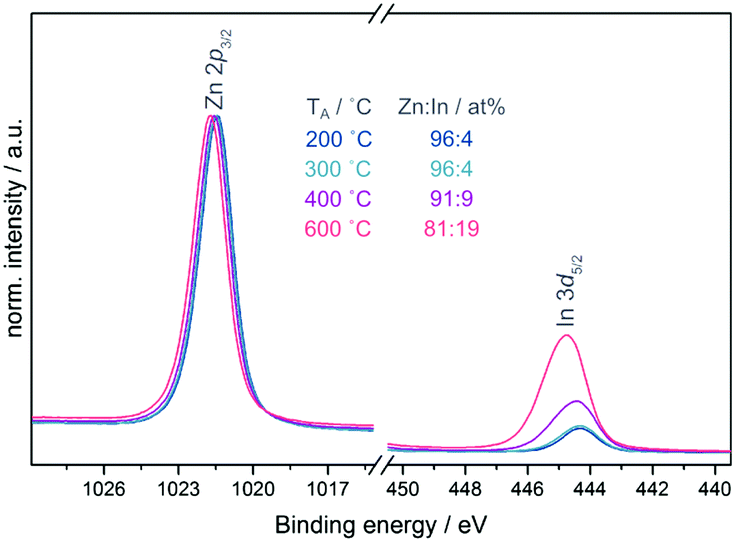 | ||
Fig. 3 Zn 2p3/2 and In 3d5/2 core level XPS spectra of the In2O3/ZnO bilayer samples annealed at varying temperatures TA plotted over the same intensity range. The table inset shows the annealing temperature and the observed Zn![[thin space (1/6-em)]](https://www.rsc.org/images/entities/char_2009.gif) :In ratios in atomic percent (at%). :In ratios in atomic percent (at%). | ||
Using a simple mathematical model which takes into account the layer thickness, surface and interface roughness, indium and zinc interdiffusion, and the IMFP of ZnO, it can be shown that the increase of the In 3d core level intensity is caused by the increase of both surface roughness and interdiffusion at higher temperatures (see ESI†). The shift in energy position suggests a change in the direct chemical environment of In, e.g. differences in oxygen coordination of In caused by varying concentration of oxygen vacancies.
With an increase in the annealing temperature the Zn 2p3/2 core level shifts consecutively to higher binding energy from 1021.5 to 1021.8 eV as shown in Fig. 3. It is not possible to distinguish between different Zn compounds using the core level alone as it shows very minute chemical shifts which cannot be resolved in XPS. Nevertheless, an increase in binding energy could indicate increased oxidation of the Zn. The Zn L3M4,5M4,5 Auger line (see ESI,† Fig. S2) confirms the presence of ZnO, showing structural features and energy positions that agree well with data reported for ZnO in the literature.26,27 Three features of the Auger line can be resolved: 3F at 495 eV, a combination of 1G, 3P, 1D at 498.4 eV and 1S at 503.0 eV.
The O 1s core level for both single and heterojunction samples shows two resolved components (see Fig. 2(b) and (d)). The lower binding energy peaks at 530.0 eV for the single layer and 530.3 eV for the bilayer can be assigned to In2O3 and ZnO, respectively.24,28 The contribution towards higher binding energy (labelled with an asterisk in the figures) which can be assigned to hydroxide groups in the layers decreases in intensity, with an increase in annealing temperature in both groups, and is more pronounced in the single layers. The ratios of the main peak to this higher binding energy contribution range from 50:50 (In2O3 single layer) and 74:26 (In2O3/ZnO bilayer) at 200 °C, to 72:28 (In2O3 single layer) and 86:14 (In2O3/ZnO heterojunction) at 600 °C. This result indicates that with increasing temperature a higher amount of unreacted hydroxide-related precursor material is converted into pure metal oxide material through condensation reactions. Hence the quality of the semiconductor in terms of purity and composition is improved as observed in previous investigations.7,29 In addition, small contributions from the oxidised Si substrate are found in survey spectra (see ESI,† Fig. S3), which also contribute to the overall oxygen signal. In addition to the analysis of core and Auger levels, XPS was used to study the electronic structure of the samples by measuring valence band spectra as depicted in Fig. 4. The In2O3 single layer shows a valence band structure typical for In2O3 with 5 resolved features, denoted by Roman numerals I–V.23,30 Whilst feature I is dominated by O 2p states, features II–IV involve mixing between the O 2p and In 5p (II and III) and 5s (IV) states. Feature V below the main VB is due to water adsorbed to the sample surface.31
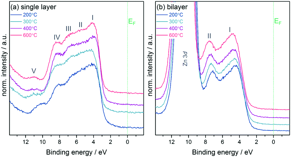 | ||
| Fig. 4 XPS valence band spectra of (a) the In2O3 single layer and (b) the In2O3/ZnO bilayer samples annealed at varying temperatures TA. Roman numerals indicate major features of the valence bands. The position of the Fermi level EF is indicated in the figures. | ||
The spectra for the In2O3/ZnO heterostructures show, besides the shallow Zn 3d core level at the bottom of the valence band (BE = 10.5 eV), two features typical for ZnO.32 From all valence band spectra the separation Δ between the valence band maximum VBmax and the Fermi energy EF was extracted by linear fits (see ESI,† Fig. S4 for exemplary fits for samples annealed at 600 °C). Table 1 summarises the values. For both sample groups the separation increases with annealing temperature with values being generally larger for the double layers.
| T A (°C) | Δ In2O3 single layer (eV) | Δ In2O3/ZnO heterojunction (eV) |
|---|---|---|
| 200 | 2.57 | 2.67 |
| 300 | 2.74 | 2.74 |
| 400 | 2.67 | 2.78 |
| 600 | 2.77 | 2.93 |
The impact of the morphological and chemical changes observed in In2O3 and In2O3/ZnO systems, on the electron transport properties, was studied using electrical field-effect measurements. Fig. 5 shows representative transfer characteristics measured for In2O3 and In2O3/ZnO transistors annealed at different temperatures in the range of 200–600 °C. Key transistor parameters including, electron mobility (μe), channel current on/off ratio (on/off), threshold voltage (VTh) and switch-on voltage (Von), are summarized in Table 2. The most important outcome of these measurements is the improved performance observed for all isotype In2O3/ZnO heterostructure devices when compared to single layer In2O3 transistors. For instance, hysteresis effects observed in In2O3 transistors annealed at 200 °C (Fig. 5(a)) are almost absent in heterojunction devices (Fig. 5(b)). Additionally, the VTh for all In2O3/ZnO transistors shifts towards more negative voltages, indicating the presence of a higher concentration of mobile electrons. More importantly, the electron mobility increases to a maximum value of 47.9 cm2 V−1 s−1 for transistors annealed at 400 °C, followed by a small reduction at higher annealing temperatures (Fig. 6). For comparison, mobility values of ZnO single layer devices annealed at different temperatures are also presented in Fig. 6.
 | ||
| Fig. 5 Transfer characteristics of thin-film transistors based on: (a) single layer In2O3, and (b) In2O3/ZnO heterojunction channels annealed at various temperatures. The insets show the respective device architecture employed. | ||
| Semiconductor | μ sat (cm2 V−1 s−1) | On/off ratio | V Th (V) | V on (V) |
|---|---|---|---|---|
| In2O3 (200 °C) | 0.3 (±0.1) | 1 × 10⁵ | 23.8 | 22.4 |
| In2O3 (300 °C) | 12.7 (±1.2) | 2 × 10⁶ | 10.3 | 1.2 |
| In2O3 (400 °C) | 30.1 (±1.3) | 4 × 10⁵ | 3.2 | −5.3 |
| In2O3 (600 °C) | 37.9 (±2.1) | 1 × 10⁴ | −0.3 | −8.6 |
| In2O3/ZnO (200 °C) | 2.9 (±0.2) | 5 × 10⁶ | 9.4 | 3.2 |
| In2O3/ZnO (300 °C) | 17.8 (±0.4) | 6 × 10³ | 1.5 | −6.2 |
| In2O3/ZnO (400 °C) | 47.9 (±0.9) | 3 × 10⁴ | −3.1 | −10.4 |
| In2O3/ZnO (600 °C) | 33.1 (±1.0) | 2 × 10³ | 1.8 | −6.4 |
 | ||
| Fig. 6 Evolution of the field-effect electron mobility (μe) measured in saturation for transistor based on single layers of In2O3 and ZnO as well as In2O3/ZnO heterojunctions as a function of annealing temperature. | ||
The clockwise hysteresis observed in the transfer curves of transistors annealed at lower temperatures is attributed to charge carrier trapping at the dielectric/semiconductor interface due to the presence of chemical defects.33 To this end, the increased amount of hydroxyl groups in the low temperature annealed layers observed in the XPS measurements is believed to act as electron trapping sites causing the hysteresis.34 With increasing annealing temperature hysteresis becomes less pronounced due to the reduction of the hydroxyl group concentration. In case of the heterojunction devices annealed at 200 °C we believe that the presence of a higher concentration of mobile electrons results in the filling of the trap states which in turn significantly reduces the operating hysteresis effects as compared to single layer In2O3 devices.
Single layer In2O3 transistors exhibit a steady increase in μe with increasing temperature. This is attributed to an improved conversion of the precursor material to In2O3 at higher temperatures, as indicated by the XPS measurements. The same holds for In2O3/ZnO heterojunctions for annealing temperatures in the range from 200 °C to 400 °C. However, in the latter type of devices the μe drops below that of single layer In2O3 transistors when annealed at 600 °C (Fig. 6), and VTh shifts back to more positive gate voltages (Fig. 5(b)). The deterioration of electrical performance is thought to originate from the increase in heterointerface roughness and the possible interdiffusion of indium and zinc atoms, as indicated by the AFM and XPS analysis. The interdiffusion processes most likely alters the local electronic properties of the semiconductors, whereas the increased In2O3 layer roughness degrades the electron transport at the vicinity of the all-important oxide heterointerface. To this end, Lin et al., has recently argued that the formation of a high quality In2O3/ZnO heterointerface is at the heart of the enhanced μe observed.21 In the latter study, it was shown that the large conduction band offset between In2O3 and ZnO leads to the formation of a quasi-2D electron gas in a process similar to that observed in high electron mobility transistors based on III–V heterostructure channels.22 The confined charge shifts the Fermi energy closer to the conduction band edge which in turn allows access to extended high mobility states. However, further dedicated effort would be required to elucidate the exact nature of the In2O3/ZnO heterojunctions, especially those subjected to high temperature post-deposition annealing steps.
Finally, for all types of devices higher annealing temperatures lead to higher channel conductivity due to increased mobility and as a consequence to higher lateral leakage currents which reduce the channel on/off current ratio. It should be noted that the active semiconductor channels in the devices discussed in Fig. 5 and 6 were not patterned and as such the relatively large lateral gate leakage currents observed directly influence the off-state current of these devices. However, this issue can be rectified by patterning the transistor channel using standard photolithography. The latter step reduces the channel off-current by nearly 2 orders of magnitude leading to a dramatic improvement in the on/off current ratio (see ESI,† Fig. S5).
In summary, single layer In2O3 and isotype In2O3/ZnO heterojunction transistors were successfully grown via spin coating in air and the influence of post-deposition annealing temperature was investigated. In the case of In2O3 transistors, it was shown that the electron mobility increases continuously with increasing annealing temperature up to 600 °C reaching a maximum value of 37.9 cm2 V−1 s−1. The electron mobility could be further increased to 47.9 cm2 V−1 s−1 by sequentially depositing In2O3 and ZnO to form low-dimensional (<14 nm-thick) In2O3/ZnO heterostructure channel transistors. Unlike single layer In2O3 transistors, however, the improved performance of the latter devices was obtained at the significantly lower annealing temperature of 400 °C. Analysis of the heterojunction channel morphology following post-deposition thermal annealing, reveals that the surface roughness and possible elemental interdiffusion/alloying/recrystallization processes may all play critical roles. On the basis of these results, we conclude that improvements in deposition methods coupled with an improved understanding of their chemical and physical characteristics, could enable further improvement in the performance of heterojunction metal oxide transistors to levels on par with, or beyond, incumbent TFT technologies but with the added advantage of low-cost, large-area manufacturing.
Acknowledgements
This work was funded by the People Programme (Marie Curie Actions) of the European Union's Framework Programme Horizon2020: “Flexible Complementary Hybrid Integrated Circuits” (FlexCHIC), grant agreement no. 658563. A. R. and D. J. P. acknowledge support from the EPSRC (EP/K004913/1 and EP/J021199/1). D. J. P. acknowledges support from the Royal Society (UF100105).References
- E. Fortunato, P. Barquinha and R. Martins, Adv. Mater., 2012, 24, 2945 CrossRef PubMed.
- S. R. Thomas, P. Pattanasattayavong and T. D. Anthopoulos, Chem. Soc. Rev., 2013, 42, 6910 RSC.
- Y. Fukui, M. Shibata, Y. Tanaka, K. Okumoto, K. Morita, K. Otake, A. K. Tripathi, B. van der Putten, J.-L. van der Steen, K. Tempelaars, L. van Leuken, F. Li, I. Yakimets, G. Gelinck, K. Myny, S. Smout, M. Willegems, S. Schols, S. Steudel, J. Genoe and P. Heremans, SID Symp. Dig. Tech. Pap., 2013, 44, 2168 Search PubMed.
- Y. S. Lee, J. Heo, S. C. Siah, J. P. Mailoa, R. E. Brandt, S. B. Kim, R. G. Gordon and T. Buonassisi, Energy Environ. Sci., 2013, 6, 2112 CAS.
- W. Z. Xu, Z. Z. Ye, Y. J. Zeng, L. P. Zhu, B. H. Zhao, L. Jiang, J. G. Lu, H. P. He and S. B. Zhang, Appl. Phys. Lett., 2006, 88, 173506 CrossRef.
- H. Bong, W. H. Lee, D. Y. Lee, B. J. Kim, J. H. Cho and K. Cho, Appl. Phys. Lett., 2010, 96, 192115 CrossRef.
- Y. H. Hwang, J.-S. Seo, J. M. Yun, H. J. Park, S. Yang, S.-H. Ko Park and B.-S. Bae, NPG Asia Mater., 2013, 5, e45 CrossRef CAS.
- S. R. Thomas, G. Adamopoulos, Y.-H. Lin, H. Faber, L. Sygellou, E. Stratakis, N. Pliatsikas, P. A. Patsalas and T. D. Anthopoulos, Appl. Phys. Lett., 2014, 105, 092105 CrossRef.
- G. Huang, L. Duan, G. Dong, D. Zhang and Y. Qiu, ACS Appl. Mater. Interfaces, 2014, 6, 20786 CAS.
- J. H. Noh, S. Y. Ryu, S. J. Jo, C. S. Kim, S.-W. Sohn, P. D. Rack, D.-J. Kim and H. K. Baik, IEEE Electron Device Lett., 2010, 31, 567 CrossRef CAS.
- Dhananjay and C.-W. Chu, Appl. Phys. Lett., 2007, 91, 132111 CrossRef.
- H. I. Yeom, J. B. Ko, C.-S. Hwang, S. Cho and S.-H. K. Park, SID Symp. Dig. Tech. Pap., 2015, 46, 52 CrossRef CAS.
- J. S. Lee, Y.-J. Kwack and W.-S. Choi, ACS Appl. Mater. Interfaces, 2013, 5, 11578 CAS.
- H. Faber, Y.-H. Lin, S. R. Thomas, K. Zhao, N. Pliatsikas, M. A. McLachlan, A. Amassian, P. A. Patsalas and T. D. Anthopoulos, ACS Appl. Mater. Interfaces, 2015, 7, 782 CAS.
- R. L. Weiher, J. Appl. Phys., 1962, 33, 2834 CrossRef CAS.
- S.-Y. Han, G. S. Herman and C.-h. Chang, J. Am. Chem. Soc., 2011, 133, 5166 CrossRef CAS PubMed.
- H. S. Kim, P. D. Byrne, A. Facchetti and T. J. Marks, J. Am. Chem. Soc., 2008, 130, 12580 CrossRef CAS PubMed.
- A. Walsh, J. L. F. Da Silva, S.-H. Wei, C. Körber, A. Klein, L. F. J. Piper, A. DeMasi, K. E. Smith, G. Panaccione, P. Torelli, D. J. Payne, A. Bourlange and R. G. Egdell, Phys. Rev. Lett., 2008, 100, 167402 CrossRef PubMed.
- P. D. C. King, T. D. Veal, D. J. Payne, A. Bourlange, R. G. Egdell and C. F. McConville, Phys. Rev. Lett., 2008, 101, 116808 CrossRef CAS PubMed.
- K. H. L. Zhang, R. G. Egdell, F. Offi, S. Iacobucci, L. Petaccia, S. Gorovikov and P. D. C. King, Phys. Rev. Lett., 2013, 110, 056803 CrossRef CAS PubMed.
- Y.-H. Lin, H. Faber, J. G. Labram, E. Stratakis, L. Sygellou, E. Kymakis, N. A. Hastas, R. Li, K. Zhao, A. Amassian, N. D. Treat, M. McLachlan and T. D. Anthopoulos, Adv. Sci., 2015, 2, 2198 Search PubMed.
- J. G. Labram, Y.-H. Lin and T. D. Anthopoulos, Small, 2015, 11, 1613 CrossRef PubMed.
- C. Körber, V. Krishnakumar, A. Klein, G. Panaccione, P. Torelli, A. Walsh, J. L. F. Da Silva, S.-H. Wei, R. G. Egdell and D. J. Payne, Phys. Rev. B: Condens. Matter Mater. Phys., 2010, 81, 165207 CrossRef.
- R. Henríquez, E. Muñoz, E. A. Dalchiele, R. E. Marotti, F. Martín, D. Leinen, J. R. Ramos-Barrado and H. Gómez, Phys. Status Solidi A, 2013, 210, 297 CrossRef.
- S. Tanuma, C. J. Powell and D. R. Penn, Surf. Interface Anal., 1994, 21, 165 CrossRef CAS.
- S. P. Kowalczyk, R. A. Pollack, F. R. McFeely, L. Ley and D. A. Shirley, Phys. Rev. B: Solid State, 1973, 8, 2387 CrossRef CAS.
- G. Schön, J. Electron Spectrosc. Relat. Phenom., 1973, 2, 75 CrossRef.
- V. Dimitrov and T. Komatsu, J. Solid State Chem., 2002, 163, 100 CrossRef CAS.
- C.-H. Choi, S.-Y. Han, Y.-W. Su, Z. Fang, L.-Y. Lin, C.-C. Cheng and C.-H. Chang, J. Mater. Chem. C, 2015, 3, 854 RSC.
- P. D. C. King, T. D. Veal, F. Fuchs, C. Y. Wang, D. J. Payne, A. Bourlange, H. Zhang, G. R. Bell, V. Cimalla, O. Ambacher, R. G. Egdell, F. Bechstedt and C. F. McConville, Phys. Rev. B: Condens. Matter Mater. Phys., 2009, 79, 205211 CrossRef.
- S. Eriksen, P. D. Naylor and R. G. Egdell, Spectrochim. Acta, Part A, 1987, 43A, 1535 CrossRef CAS.
- P. D. C. King, T. D. Veal, A. Schleife, J. Zúñiga-Pérez, B. Martel, P. H. Jefferson, F. Fuchs, V. Muñoz-Sanjosé, F. Bechstedt and C. F. McConville, Phys. Rev. B: Condens. Matter Mater. Phys., 2009, 79, 205205 CrossRef.
- C. Zhu, A. Liu, G. Liu, G. Jiang, Y. Meng, E. Fortunato, R. Martins and F. Shan, J. Mater. Chem. C, 2016, 4, 10715 RSC.
- J.-S. Seo, J.-H. Jeon, Y. H. Hwang, H. Park, M. Ryu, S.-H. K. Park and B.-S. Bae, Sci. Rep., 2013, 3, 2085 Search PubMed.
Footnote |
| † Electronic supplementary information (ESI) available. See DOI: 10.1039/c6tc04907a |
| This journal is © The Royal Society of Chemistry 2017 |