Self-cleaning antireflective coating with a hierarchical texture for light trapping in micromorph solar cells
Received
25th July 2016
, Accepted 22nd November 2016
First published on 22nd November 2016
Abstract
Surface texture plays a particularly important role in surface behaviors. Herein, we report a novel hierarchical texture combining microcone arrays with nanopits for minimizing the reflection loss at the air/glass interface. Its optical properties were confirmed via spectral characterization (reflectance, transmittance and haze) and FDTD numerical simulation. The results reveal that nanopits provide a gradient index profile for improving index discontinuity and are advantageously antireflective in a shorter wavelength while microcone arrays allow multi-reflection for light scattering and prevail over a longer wavelength region. The hierarchical texture resulting from the combination of both exhibits dramatic broadband light trapping over the entire visible spectrum. Moreover, without fluorosilane modification, the hierarchical texture allows a superhydrophobic surface (contact angle of ca. 136°) due to its higher roughness. The light trapping performance of the hierarchical texture onto the front glass surface of the micromorph cell was investigated by photoelectrical current–voltage curves and external quantum efficiency spectra. The results indicate that both the number of trapped photons and their optical path length in the absorbed layer are increased, thereby achieving an overall efficiency of 11.44% out of the bare device of 10.93% efficiency, resulting in a 4.7% enhancement. Additionally, the proposed method paves a promising way for light trapping in other solar applications, owing to its advantages of large area, low cost and facile fabrication.
Introduction
Due to greatly reduced silicon material consumption and the feasibility of fabricating solar cells on inexpensive large-area foreign substrates (glass, ceramics or plastic etc.), a lot of research has been focused on thin film silicon solar cells.1,2 In particular, a micromorph solar cell, which is based on stacks of amorphous top cells with a high band gap, and a microcrystalline bottom cell with a low band gap enhance the photocurrent due to much better utilization of the solar spectrum and higher light harvesting.3,4 However, according to Fresnel equations, assuming flat interfaces and neglecting interference effects, primary reflections of more than 4% at the air/glass interface and 2% at the glass/transparent conductive oxide (TCO) interface still exist because of refractive index discontinuity (glass ∼ 1.5, TCO ∼ 2.0, air ∼ 1.0).5 These optical losses seriously restrict further improvement in the cell performance. To solve this problem, a lot of strategies have been proposed for reflection suppression. In general, mechanisms can be categorized into three types. One approach is related to destructive interference by a single-layer dielectric thin film coating with an odd number of quarter wavelengths. But it is not suitable for broadband antireflection due to the highly wavelength-dependent nature.6 Besides, the reflectance of a surface is a sensitive function of its roughness and topography; with this knowledge, the conception of texture with an appropriate structure is of great significance for reflection suppression. On the one hand, based on geometrical optics, when the feature dimension of the texture is comparable to or larger than the incident wavelength, the microtexture allows the multiple rebounds of the incoming light to manipulate light trapping.7,8 The spectral independence of antireflection is the main advantage of the microtextures.9 Commonly, fabrication of microtexture can be completed via photolithograph, chemical wet or dry etching processes.10 On the other hand, as referred to as the gradient refractive index theory,11 when the feature size of the texture is smaller than the incident wavelength, it can serve as an inhomogeneous layer with a gradient refractive index to improve the index discontinuity,12 and thus reduce the reflectance. Successful fabrication of the graded-index antireflective texture has been achieved by nanostructures at the interfaces.13,14 Most typically, the natural “moth-eye” with nano-scale nipple arrays has been reproduced precisely using interference lithographic techniques for the antireflective coating and used commercially on solid plastic and other lenses.15 Very recently, a concept utilizing hierarchical texture combining both the large (micro) and small (nano) structures is expected to realize optimal photon management.16,17 As exemplified by the crystalline silicon production, nanotexturing on the micropyramidal surfaces to form a hierarchical structure, which is fabricated through noble metal (Au or Ag) assisted chemical etching, has been extensively explored for low reflection.18–21 However, the conception of hierarchical texture with micro/nanostructures on transparent glass substrates for light management has still been less-frequently addressed. Moreover, the realization of a directly patterned texture on the glass surface using photolithography patterning and wet/dry etching processes leads to an increase in complexity and cost in the fabrication processes. To avoid this problem, ultraviolet (UV) nanoimprint lithography (NIL) provides an alternative way to pattern the surface of the glass.22,23 Fundamentally, UV-curable polymers with a suitable refractive index are indispensable for the fabrication of the textured replicas. If the refractive index of the polymer is lower than that of glass, it can modify the refractive index profile and further decrease the surface reflection. Although the texture mold is also prepared via lithography patterning and etching processes, once replica stamps are made, they can be repeatedly utilized for pattern transfer into secondary substrates. Furthermore, industrial-scale mass fabrication techniques (i.e., a step and flash technique24) have been developed in soft imprint lithography, which would facilitate mass-production for industrial applications. Meanwhile, exemplified by the ‘lotus effect’, another important property of hierarchical texture, hydrophobicity, has much to do with its roughness; increasing surface roughness can remarkably enhance surface water repellency or self-cleaning performance.25 Therefore, one well-designed hierarchical texture can not only eliminate the reflection losses but also provide low-cost maintenance due to its self-cleaning properties.
Motivated by these, a hierarchical texture combining nanopits with microcone arrays was proposed for optical light management and superficial self-cleaning. The hierarchical textured glass shows lower reflection, higher scattering, a broader spectral region, and a higher contact angle than single scale textured glass. Without modifying the cell configuration, we simply imprinted this hierarchical texture onto the front surface of the cell device for light trapping. As confirmed by current–voltage curves and external quantum efficiency spectra, an overall efficiency enhancement of 4.7% was achieved in comparison with the bare device.
Experimental
Preparation of textures
Three types (nano, micro and hierarchical) of textures were prepared. Nanoroughness was generated on the surface of the microcone arrays to form a “hierarchical” texture via Al anodization nanotechnology,26 as indicated in Fig. 1. Put simply, one sapphire mold with flat-top cone arrays was used as the basic “micro” texture, and then a layer of an Al film (ca. 500 nm) was evaporated on its surface at a very slow rate of 5 Å s−1. Next, the Al layer was anodized in 0.1 mol L−1 H3PO4 solution at 195 V and 0 °C for 3 min, followed by soaking in H3PO4 solution (5 wt%) for 55 min at 45 °C to widen the feature dimension of the nanostructure. By comparison, an Al layer covered on a smooth glass was anodized under the same conditions, referred to as a “nano” texture.
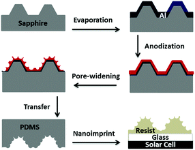 |
| | Fig. 1 Schematic fabrication of the hierarchical texture and transfer of its pattern onto the front glass surface of the cell device. | |
Synthesis of UV-curable resist
A mixture of (3-mercaptopropyl) trimethoxysilane, HCl (37 wt%) and methanol (volume ratio, 1![[thin space (1/6-em)]](https://www.rsc.org/images/entities/char_2009.gif) :2:12) was stirred at 90 °C for 24 h to produce polyhedral oligomeric silsesquioxanes (POSS-SH). Then, purified POSS-SH were interacted with 1H,1H,2H,2H-perfluorooctyl acrylate (CFA6) monomers to obtain POSS-SH-F under 365 nm UV light for 6 h. The solvent was removed using a rotary evaporator and purified repeatedly. The UV-curable resist was a hybrid of the initiator (I-907), solvent (CH2Cl2), POSS-SH-F and the crosslinker (2,2,3,3,4,4,5,5-octafluoro-1,6-hexyldiacrylate, DCFA4) (mole ratio, 1:16).
:2:12) was stirred at 90 °C for 24 h to produce polyhedral oligomeric silsesquioxanes (POSS-SH). Then, purified POSS-SH were interacted with 1H,1H,2H,2H-perfluorooctyl acrylate (CFA6) monomers to obtain POSS-SH-F under 365 nm UV light for 6 h. The solvent was removed using a rotary evaporator and purified repeatedly. The UV-curable resist was a hybrid of the initiator (I-907), solvent (CH2Cl2), POSS-SH-F and the crosslinker (2,2,3,3,4,4,5,5-octafluoro-1,6-hexyldiacrylate, DCFA4) (mole ratio, 1:16).
Fabrication of solar cells
A micromorph silicon solar cell was deposited on a glass substrate (3.2 mm) by using a conventional plasma enhanced chemical vapor deposition (PECVD) technique, with superstrate configuration: glass/AZO/a-Si(p–i–n)/μc-Si(p–i–n)/AZO/Ag. The thicknesses of the amorphous silicon top cell and the microcrystalline silicon bottom cell were 0.26 μm and 1.2 μm. The front (500 nm) and rear (100 nm) electrodes were deposited via AZO transparent film layers. Finally, a layer of Ag (100 nm) was covered on the cell as the back reflector, with an active area of 0.52 cm2.
Procedures of UV NIL
Firstly, transparent soft stamps were accurately produced in an inverse manner by pouring a mixture of the polydimethylsiloxane (PDMS) pre-polymer and its curing agent (10:1 by weight) onto textures. After squeezing the bubbles out under a vacuum, they were cured for 4 h at 70 °C in an oven before careful separation. In advance, to improve the adhesion strength between the glass and the UV-curable resist, the surfaces of the glass substrate were modified by soaking them in 0.2 wt% 3-(methacryloyloxy) propyltrimethoxysilane in toluene for 24 h. After cleaning in ethanol and drying in air, the glass was spin-coated with a 3 μm thick UV-curable resist at 1000 rpm for 15 s. Then, the sandwich sample (soft stamp/resist/glass) was impacted by applying a pressure of 0.03 MPa for 10 min and exposed to UV light for 10 min. Finally, the texture could be easily detached from the soft stamp due to the fluorinated groups of the resist and appeared on glass with high fidelity. Using the same procedures, a planar UV-curable resist layer was imprinted on glass, named as “flat” texture. Bare glass was used as a reference, named as “bare”.
Characterization
The 1H-NMR spectrum was recorded on a Varian Mercury Plus-400 NMR spectrometer (400 MHz) with CDCl3 as the deuterated solvent. The refractive index (n) and the absorption index (k) of the resist film were measured using NKD-8000 (Aquila, UK) equipment. Field emission scanning electron microscopy (FE-SEM, ULTRA 55, Carl Zeiss AG, Germany) images were all obtained at a low incident electron voltage of 5 kV. Morphologies were scanned under ambient conditions using a Dimension Icon AFM (Bruker, Germany). The thickness of the texturing resist film was measured using a surface profile measuring instrument (Dekatk 150, Veeco, USA). Reflectance and transmittance spectra were measured using a UV/VIS/NIR spectrophotometer (Lambda-750S, PerkinElmer, USA) with an integrating sphere (60 mm) attachment over the range of 370–1000 nm. Contact angle measurements were recorded on a spinning drop interface tensiometer (SL200C, KINO Industry, USA) and the volume of the individual deionized water droplet was kept constant at 5 μL. External quantum efficiency (EQE) curves for the component top and bottom cells were measured using a QEX10 Quantum Efficiency Measurement System (PV Measurements, USA). Current–voltage curves of the solar cells were characterized using a solar simulator under standard test conditions (AM 1.5 G, 100 mW cm−2 and 25 °C).
Numerical simulation
Numerical simulations by using the finite-difference-time-domain (FDTD) method were performed to explain how the incoming light interacts with different textures, by assuming that the light passes through the glass only once. Perfectly matched layers (PML) and periodic boundary conditions were used in the perpendicular and horizontal directions. The thickness of the texturing resist film was equivalent to 3 μm. Topographies of textures, measured using AFM, were directly imported into FDTD simulation. A plane wave source ranging from 370 to 1000 nm was used to illuminate these textures at the normal incidence. Optical data (n and k) of the resist in the simulation were input from the measured results and the glass substrate had a constant value (n = 1.5, k = 0). A 2D z-normal frequency-domain field (DFT) power monitor was placed above the wave source to obtain the reflectance spectra and one x-normal DFT profile monitor was set to obtain the spatial distribution of the electromagnetic field.
Results and discussion
Characterization of the UV resist
In Fig. 2(a), through a photo-click ‘‘thiol–ene’’ reaction, half thiol groups of POSS-SH were grafted to CFA6 monomers to obtain POSS-SH-F, which was confirmed using 1H-NMR. Each peak of the 1H-NMR spectrum in Fig. 2(c) is correspondingly assigned to the related proton, which agrees well with previous results.27 Under UV light irradiation, a transparent resist film with a thickness of 1 mm was cured. Some physical properties of the cured resist film, such as hardness, surface energy and Young's modulus, can be found in ref. 27. Here, we focus on its optical properties. In Fig. 2(b), the refractive index (n) is in the 1.48–1.5 range in the entire visible range, which is slightly lower than that of glass (ca. 1.5). Moreover, the transmittance is higher than 90% in Fig. 2(d) (typically 95% around 450 nm). Due to the similar refractive index and high transmittance to glass, the UV-curable resist is a good candidate as a material for texture transfer on a glass substrate.
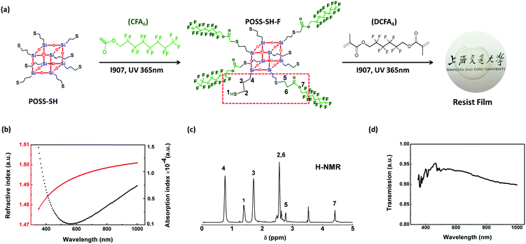 |
| | Fig. 2 (a) Illustration of “thiol–ene” photo-polymerization; (b) the refractive index (red line) and the absorption index (black line) of the resist film as a function of wavelength; (c) 1H-NMR spectrum of POSS-SH-F in CDCl3; (d) transmittance spectrum of the resist film with a thickness of 1 mm. | |
Surface characterization
Countless mutually parallel and randomly arranged nanopores constitute the nanotexture, as observed in Fig. 3(a); and flat-top cone arrays with a good hexagonal packed arrangement are shown in Fig. 3(b).The hierarchical texture resulting from the combination of both can be described by hexagonally arranging a cone-shaped microtexture with nanopits distributed quite uniformly on its surface. More clearly, the cone with a roughened surface looks like half of a ‘golf ball’, Fig. 1(c). Textures were imprinted on the glass substrates using UV NIL and their morphologies were scanned using AFM and were called ‘‘Flat’’, “nano”, “micro”, and “hierarchical”, respectively. As measured using a surface profiler, the thickness of the flat resist film is about 3 μm. Fig. 4(a) shows that the replicated nanotexture is occupied by random arranged nanopits. According to the histogram distribution diagrams of depth in Fig. 4(d) and diameter in Fig. 4(e), they follow the Gaussian distribution model with a calculated average value of about 112 nm and 275 nm, respectively. The imprinted microtexture in Fig. 4(b) inherits the geometrical feature, and the period of close-packed hexagonal arrangement is 3 μm. The line cross-section profiles in Fig. 4(f) tell us that the height of the replicated cone is about 1.25 μm and the diameter of the base and top are 2 and 0.8 μm. In contrast with the smooth surface of the cone in the microtexture, the surface of the cone and the interspace in the hierarchical texture are roughened evenly by nanopits. These morphological differences significantly affect the properties (optical and wettability) of the surfaces. These effects will be discussed next in detail.
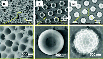 |
| | Fig. 3 Top-view SEM images: (a) ‘nano texture’ with randomly arranged nano-pores; (b) ‘micro texture’ patterned by flat-top cone arrays; (c) the ‘hierarchical texture’ of a hexagonally arranged cone shaped micropattern with nanopits distributed quite uniformly on the surface and interspace. | |
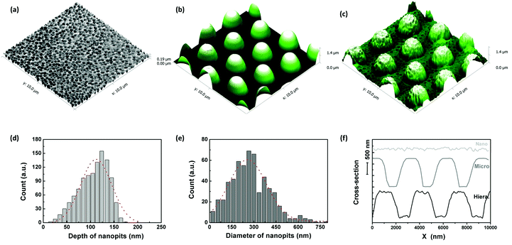 |
| | Fig. 4 Three-dimensional representation of the AFM images of the texture patterned by nanopits (a), microcone arrays (b) and hierarchical texture (c). Histogram distribution diagrams of the depth (d) and diameter (e) of nanopits by statistical analysis in a large area of 10 × 10 μm. Image (f) is the line cross-section profiles of nano, micro and hierarchical textures. | |
Optical properties
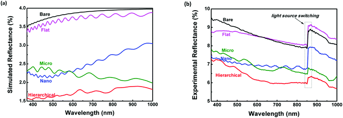
The optical properties (reflection, transmission and scattering) of different textures were investigated via spectral reflectance, total transmittance and haze as a function of wavelength from 370 to 1000 nm. Simulated reflectance spectra are shown in Fig. 5(a). Firstly, the reflectance of the glass coated with a 3 μm flat resist layer is slightly lower than that of the bare glass due to the lower refractive index of the resist material than glass. The hierarchical texture, resulting from combining both, yields a stronger broadband antireflection behavior (down to 1.7% from 3.8%) in the entire visible range. Since the reflection of the back side is not considered for simulation, while it is inevitable in the experimental measurements, there exist some quantitative differences in the reflectance values. However, the trend of experimental reflectance on different textured glasses in Fig. 5(b) agrees qualitatively with the simulation results. Typically, compared with bare glass, the average reflectance in the range from 600 to 800 nm of hierarchical textured glass decreases from 8.3% to 6%, which is lower than the values of the microtexture (6.8%) and nanotexture (6.6%). Moreover, the decrease in the experimental value between the bare and hierarchical textured glass is in quite good agreement with the simulation result. Additionally, not only the simulated spectra but also the experimental results unanimously reveal that the antireflective performance of the nanopit is more effective in the range of short wave (shorter than 600 nm) while that of the microcone arrays prevails over a longer wavelength (longer than 600 nm). As for glass, except negligible absorbance, the suppression of reflectance means the enhancement of transmission. The transmittance spectra are shown in Fig. 6(a). Indeed, compared with the bare glass, the transmittance in the entire spectrum of the hierarchical textured glass was greatly enhanced. This enhancement of transmittance can be explained by several effects. For one thing, the cone array at the microscale provides an antireflective effect due to strong forward scattering and light angular redistribution. As the light strikes the cone, it diffracts to several beams and partly rebounces between cones, preventing light from escaping back to air. For another, as introducing nanopits on the surface of the cone and interspace between cones, these nanopits behave as an effective medium, further improving the impedance mismatch of the refractive index. Moreover, reflection suppression may also occur by destructive interferences of light with partially different phases.28
 |
| | Fig. 5 Simulated (a) reflectance spectra without considering the reflection of the glass back side; experimental (b) reflectance spectra of glass covered with different textures. | |
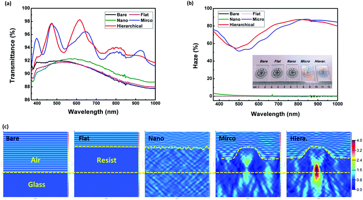 |
| | Fig. 6 Total transmittance (a) and haze (b) of glass with different textures as a function of wavelength from 370 to 1000 nm and its entity pictures; vertical section (c) of the simulated electric field intensity at a wavelength of 518 nm. | |
The spectral haze value, which is defined by the ratio of the diffuse to the total transmission, is one of the most crucial parameters to be taken into account for controlling the light behavior in the diverse optical and optoelectronic systems,29 as shown in Fig. 6(b). According to Fig. 4(e), the average diameter of the nanopits is about 275 nm, which is smaller than the measuring wavelength (370–1000 nm). The longer light cannot sense the structural details and the scattering and diffraction are weak, thus the haze of the nanopit textured glass is almost zero. In contrast, the haze values of glass with mirco and hierarchical textures are averaged to be 70%, which is mainly attributed to the multiple refraction and reflection of the incident light in the cone arrays with periods (3 μm) larger than the incident wavelengths. The light scattering properties are also confirmed visually in the inset of Fig. 6(b), the characteristics are extremely clear through bare glass and glass with flat and nanotextures; nevertheless, a blurry appearance is observed in the micro- and hierarchical textured glass due to their light scattering. Also, rainbow-like colors appear on their surfaces due to the strong light diffraction properties. Vertical sections of the simulated electric field intensity profile at 518 nm were carried out to gain insight into the light propagation across these textures. As shown in Fig. 6(c), the cone arrays exhibit strong light interference patterns and allow light propagation across the interface while there are no scattering lights for the bare glass and glass with a flat resist film. Obviously, the field intensities are maximized in the hierarchical texture, implying that it can increase the number of photons propagating across the interfaces. We confirmed that the enhancement in light trapping of the hierarchical texture mainly originates from two effects: the light scattering of the microcone arrays through multiple reflections and refractions, and the antireflection of the nanopits by improving the refractive index-mismatch.
Self-cleaning properties
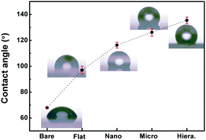
The surface self-cleaning was evaluated by measuring the water contact angle (CA). The CA of a water droplet is dependent on the ratio of the trapped air-pocket at the solid–liquid interface. Fig. 7 shows a comparison of the water CAs of glass with different textures. Without any fluorosilane modification, the CA of bare glass is ca. 68 ± 0.9° and the CA of the hierarchical textured glass is 136 ± 2.5°, respectively. It is apparent that the hierarchical structure significantly enhances the hydrophobicity of the glass surface compared to that of the microcone arrays (ca. 126 ± 2.9°) and nanopits (ca. 116 ± 2.2°). The superhydrophobicity allows excellent self-cleaning behaviour.30 For the hierarchical texture, the roughness is higher than that of the micro- and nanotextures, leading to a smaller area fraction of the solid surface in contact with a liquid, which is why the hierarchical texture can enjoy a better self-cleaning state.31
 |
| | Fig. 7 Water contact angles of glass coating with different textures; insets are micrographs of water droplets. | |
Efficiency enhancement of solar cells
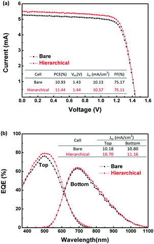
Finally, the hierarchical texture was imprinted onto the surface of micromorph solar cells to confirm its light trapping properties. The measured solar characteristics including open circuit voltage (Voc), short circuit current density (Jsc), and power conversion efficiency (PCE) are listed in Fig. 8(a). A slight variation is found in Voc and FF because texture fabrication is completed on the surface with no modification in the standard structure of the cells. Using bare cells as the reference, the PCE of the hierarchical textured cells is boosted from 10.93% to 11.44%, resulting in a 4.7% enhancement. Meanwhile, EQE, which is identical to the incident photon to converted electron ratio, was investigated to confirm the improved Jsc, as shown in Fig. 8(b). Compared to the bare cell, both the top and bottom component cells with the imprinted hierarchical texture have higher Jsc. According to the EQE spectra, Jsc increases from 10.18 mA cm−2 to 10.70 mA cm−2, for the top cell, and from 10.80 mA cm−2 to 11.16 mA cm−2, for the bottom cell. The relative increases for the top and bottom cells are 5.11% and 3.33%, respectively. For the tandem solar cells, the output Jsc is determined by the lowest current between the two component cells. So, these results are in excellent agreement with the current–voltage measurements (10.13 mA cm−2 of the bare cell and 10.57 mA cm−2 of the hierarchical textured cell). These enhancements are mainly attributed to the improved light trapping ability of the device by imprinting the hierarchical texture on the light entrance of the cell. Due to numerous microcones and nanopits on the textured interface, the incident light passing through it undergoes strong antireflection and scattering. The antireflection of the nanopits traps more photons and the scattering of the microcone array changes the propagation direction of the photon from normal to oblique incidence in the cell. Consequently, the number of photons is increased and the optical path length is also elongated, hence light absorption in the active layer is undoubtedly enhanced. By the way, the coating with hierarchical antireflective texture is not merely limited to micromorph solar cell; it can be implemented on the other solar applications and allows mass production by step and repeat imprint lithography, which has great significance in the photovoltaic industry.
 |
| | Fig. 8 (a) Current–voltage curves of bare and hierarchical textured cell under standard test conditions (AM 1.5 G, 100 mW cm−2 and 25 °C); (b) external quantum efficiency curves for the component top and bottom cells. | |
Conclusions
In conclusion, we have fabricated the hierarchical texture composed of microcone arrays and nanopits. It exhibits an excellent broadband light trapping performance over the entire visible range. By imprinting the hierarchical texture as the front antireflective coating, the efficiency of micromorph solar cells achieves a 4.7% enhancement. It also provides low-cost maintenance due to self-cleaning properties. This approach provides a facile, efficient and inexpensive light trapping strategy to a wide variety of high-performance optoelectronic devices.
Acknowledgements
This research was supported by the State High-Tech Development Plan of China (863 Program, Grant No. 2011AA050518).
References
- A. G. Aberle, Thin Solid Films, 2009, 517, 4706–4710 CrossRef CAS.
- A. V. Shah, H. Schade, M. Vanecek, J. Meier, E. Vallat-Sauvain, N. Wyrsch, U. Kroll, C. Droz and J. Bailat, Prog. Photovoltaics Res. Appl., 2004, 12, 113–142 CrossRef CAS.
- K. Yamamoto, A. Nakajima, M. Yoshimi, T. Sawada, S. Fukuda, T. Suezaki, M. Ichikawa, Y. Koi, M. Goto, T. Meguro, T. Matsuda, M. Kondo, T. Sasaki and Y. Tawada, Sol. Energy, 2004, 77, 939–949 CrossRef CAS.
- J. Krc, F. Smole and M. Topic, J. Non-Cryst. Solids, 2006, 352, 1892–1895 CrossRef CAS.
- F. Meillaud, A. Billet, C. Battaglia, M. Boccard, P. Cuony, M. Despeisse, L. Ding, J. Escarre-palou, H. Simon, L. Linus, S. Nicolay, G. Parascandolo, M. E. St and C. Ballif, IEEE J. Photovoltaics, 2012, 2, 236–240 CrossRef.
- F. Yan, E. P. J. Parrott, X. D. Liu and E. Pickwell-MacPherson, Opt. Lett., 2015, 40, 2886–2889 CrossRef PubMed.
- J. Li, H. Yu, Y. Li, F. Wang, M. Yang and S. M. Wong, Appl. Phys. Lett., 2011, 98, 021905 CrossRef.
- P. Bermel, C. Luo, L. Zeng, L. C. Kimerling and J. D. Joannopoulos, Opt. Express, 2007, 15, 16986–17000 CrossRef CAS PubMed.
- J. Escarré, K. Söderström, M. Despeisse, S. Nicolay, C. Battaglia, G. Bugnon, L. Ding, F. Meillaud, F. J. Haug and C. Ballif, Sol. Energy Mater. Sol. Cells, 2012, 98, 185–190 CrossRef.
- X. Shen, Q. Wang, P. Wangyang, K. Huang, L. Chen and D. Liu, Opt. Lett., 2015, 40, 1290–1293 CrossRef CAS PubMed.
- S. Chattopadhyay, Y. F. Huang, Y. J. Jen, A. Ganguly, K. H. Chen and L. C. Chen, Mater. Sci. Eng., R, 2010, 69, 1–35 CrossRef.
- C. Chang, J. A. Dominguez-caballero, H. J. Choi and G. Barbastathis, Opt. Lett., 2011, 36, 2354–2356 CrossRef PubMed.
- S. Chhajed, M. F. Schubert, J. K. Kim and E. F. Schubert, Appl. Phys. Lett., 2008, 93, 251108 CrossRef.
- J. Y. Chen, W. Chang, C. K. Huang and K. W. Sun, Opt. Express, 2011, 19, 14411–14419 CrossRef CAS PubMed.
- A. R. Parker and H. E. Townley, Nat. Nanotechnol., 2007, 2, 347–353 CrossRef CAS PubMed.
- W. Wei, M. Tsai, S. Ho, S. Tai, C. Ho, S. Tsai, C. Liu, R. Chung and J. He, Nano Lett., 2013, 13, 3658–3663 CrossRef CAS PubMed.
- A. Tamang, A. Hongsingthong, P. Sichanugrist, V. Jovanov, H. T. Gebrewold, M. Konagai and D. Knipp, Sol. Energy Mater. Sol. Cells, 2016, 144, 300–308 CrossRef CAS.
- D. Z. Dimitrov and C. Du, Appl. Surf. Sci., 2013, 266, 1–4 CrossRef CAS.
- Y. Liu, A. Das, Z. Lin, I. B. Cooper, A. Rohatgi and C. P. Wong, Nano Energy, 2014, 3, 127–133 CrossRef CAS.
- H. Lv, H. Shen, Y. Jiang, C. Gao, H. Zhao and J. Yuan, Appl. Surf. Sci., 2012, 258, 5451–5454 CrossRef CAS.
- Y. Cao, A. Liu, H. Li, Y. Liu, F. Qiao, Z. Hu and Y. Sang, Appl. Surf. Sci., 2011, 257, 7411–7414 CrossRef CAS.
- B. L. J. Guo, Adv. Mater., 2007, 19, 495–513 CrossRef.
- J. Y. Chen and K. W. Sun, Sol. Energy Mater. Sol. Cells, 2010, 94, 629–633 CrossRef CAS.
- T. S. Kustandi, W. W. Loh, H. Gao and H. Y. Low, ACS Nano, 2010, 4, 2561–2568 CrossRef CAS PubMed.
- M. Lee, G. Kwak and K. Yong, ACS Appl. Mater. Interfaces, 2011, 3, 3350–3356 CAS.
- W. Lee and S. Park, Chem. Rev., 2014, 114, 7487–7556 CrossRef CAS PubMed.
- H. Lin, X. Wan, X. Jiang, Q. Wang and J. Yin, J. Mater. Chem., 2012, 22, 2616–2623 RSC.
- L. K. Yeh, K. Y. Lai, G. J. Lin, P. H. Fu, H. C. Chang, C. A. Lin and J. H. He, Adv. Energy Mater., 2011, 1, 506–510 CrossRef CAS.
- G. Kang, K. Bae, M. Nam, D.-H. Ko, K. Kim and W. J. Padilla, Energy Environ. Sci., 2015, 8, 2650–2656 CAS.
- H. J. Gwon, Y. Park, C. W. Moon, S. Nahm, S. J. Yoon, S. Y. Kim and H. W. Jang, Nano Res., 2014, 7, 670–678 CrossRef CAS.
- H. Xu, N. Lu, G. Shi, D. Qi, B. Yang, H. Li, W. Xu and L. Chi, Langmuir, 2011, 27, 4963–4967 CrossRef CAS PubMed.
|
| This journal is © The Royal Society of Chemistry 2017 |


