A novel porous Ti/TiN/Ti thin film as a working electrode for back-contact, monolithic and non-TCO dye-sensitized solar cells†
Po-Shen
Shen
a,
Ming-Hsien
Li
a,
Yu-Syuan
Yang
a,
Sean
Sung-Yen Juang
a,
Chia-Wei
Lin
a,
Tan-Ya
Yin
a and
Peter
Chen
 *abc
*abc
aDepartment of Photonics, National Cheng Kung University, Tainan, Taiwan 701. E-mail: petercyc@mail.ncku.edu.tw
bResearch Center for Energy Technology and Strategy (RCETS), National Cheng Kung University, Tainan, Taiwan 701
cAdvanced Optoelectronic Technology Center (AOTC), National Cheng Kung University, Tainan, Taiwan 701
First published on 17th March 2017
Abstract
In the present work, we develop a novel method to fabricate a porous titanium–titanium nitride–titanium (Ti–TiN–Ti) thin film for use as a conducting electrode in dye-sensitized solar cells (DSCs). Three non-conventional device architectures, namely back-contact (BC-DSCs), monolithic (m-DSCs) and TCO-glass free back-contact (non-TCO BC-DSCs) dye solar cells, using this porous electrode are constructed. The back-contact dye-sensitized solar cells and monolithic dye-sensitized solar cells deliver power conversion efficiencies of 4.53% and 3.16%, respectively. In these two devices, only one piece of TCO glass is required, which has the potential to reduce the cost and weight in comparison with the traditional sandwich device. Furthermore, we present a non-TCO back-contact DSC photovoltaic device. In this case, the fabrication cost of DSCs could be greatly reduced as FTO glasses are completely absent in the device. The non-TCO BC-DSCs yielded an overall conversion efficiency of 3.53%, which is 51% of that of standard conventional DSCs with the same thickness of photoactive TiO2 layer.
Introduction
Dye-sensitized solar cells (DSCs) have received great attention due to their ease of fabrication and use of cost-effective materials. They might become promising alternatives to conventional silicon-based solar cells due to these advantages.1 Several studies have focused on the efficiency enhancement of DSCs after the milestone reported by O’Regan and Grätzel in 1991.2,3 Best conversion efficiencies of more than 13–14% for DSCs have been achieved recently.3,4 Conventional dye-sensitized liquid junction solar cells are composed of two transparent conducting fluorine-doped tin oxide (FTO) glasses with the electrolyte sandwiched between them.5 One of the substrates is coated with mesoporous titania onto which the dyes are anchored and this serves as the working electrode (WE) for light harvesting and electron collection. The other one, acting as a cathode, is platinized to form ohmic contact with the electrolyte. However, it has been reported that FTO glass is a major part of the cost in fabricating DSCs.6 Moreover, its heavy weight due to its thickness prevents the integration of DSCs with lightweight products such as portable devices and consumer electronics and in the application of the internet of things (IOTs). Therefore, the back contact (BC) concept was introduced as an alternative architecture to conventional sandwich-type DSCs in order to solve those problems.7,8 To make a back contact-DSC (BC-DSC), a porous back contact electrode (BCE) is required that allows the penetration of dye solution for adsorption on the mesoscopic TiO2 layer and the transport of electrolyte under working conditions. The first design used a porous sputtered Ti thin film to substitute the FTO layer as the electron collecting electrode.6,7 The FTO glass used for the working electrode was then replaced by a transparent plain glass substrate. Some groups reported BC-DSCs by employing a porous Ti film as the collecting electrode due to its good stability and Schottky contact behavior across the Ti/electrolyte interface.6,8–10 The Ti electrode exhibited a lower sheet resistance than the FTO layer and the electron transfer kinetics at the TiO2 film/Ti electrode interface were very similar to those at the TiO2 film/FTO interface according to electrochemical impedance spectra.9 To further enhance the energy conversion efficiency of back contact DSCs, TiCl4 treatment was adopted in order to improve the electron transport between TiO2 nanoparticles, thus leading to an increased short-circuit current density.11 It has also been observed that the charge generation profile affects the performance of BC-DSCs due to the reverse direction of electron transport and the charge collection distance.12 Those results demonstrated that absorbers with lower extinction coefficients allow a moderate drop in the carrier generation gradient which benefits the charge collection for back contact configuration. In 2010, Fu et al. proposed a new configuration of monolithic BC-DSC that was constructed with two interdigited finger-shaped electrodes on a single substrate.13,14 Kashiwa et al. and Fu et al. have reported TCO-free device architectures, consisting of a porous Ti film as the BCE and a Ti foil as the counter electrode, that completely exclude the use of FTO glasses in DSCs.10,15 Recently, Ti metal mesh was also employed as the back-contact electrode layer for its application in TCO-free back-contact dye-sensitized solar cells.16,17 Currently, Ti is the most common electrode material for BC-DSCs. Meanwhile, titanium nitride (TiN) has been confirmed to be a corrosion-resisting material in contact with the I−/I3− redox couple electrolyte and has exhibited its functionality in flexible devices.18 A long-term stability test that confirmed TiN to be more stable than Ti for dye-sensitized solar cells has also been carried out.19 Furthermore, some recent works have reported that nanostructured TiN composite films exhibit high electrical conductivity and superior electrocatalytic activity and are effective alternative counter electrodes for use in dye-sensitized solar cells.20,21 Moreover, counter electrodes prepared with TiN nanotubes and TiN micro/nano-spheres have displayed better catalytic performances than conventional Pt electrodes in contact with the I−/I3− redox couple in DSC applications.22,23 These results have implied that recombination should be suppressed if TiN is used as the working electrode. Recently, TiN has been used as a BCE for high efficiency TCO-free and flexible DSCs.24,25 In this work, we propose a novel method to fabricate a porous Ti–TiN–Ti thin film for use as the WE in BC-DSCs and monolithic DSCs. Moreover, a complete non-TCO BC-DSC photovoltaic device employing this porous BCE is also demonstrated. Dyes with different molar extinction coefficients (Z-907 and MK-2) are used to examine the influence on the energy conversion efficiencies of the BC-DSCs. The crystalline orientations of the sputtered TiN thin film were characterized using X-ray diffraction (XRD). The morphologies of the porous thin film electrodes were examined using scanning electron microscopy (SEM). UV-vis measurements were performed in order to obtain the optical properties of the sputtered Ti–TiN–Ti thin film.Experimental
Preparation of working electrodes for back-contact and monolithic DSCs
Polystyrene (800 nm, 10% wt, Sigma Aldrich) that was diluted with ethanol (volume ratio 1![[thin space (1/6-em)]](https://www.rsc.org/images/entities/char_2009.gif) :
:![[thin space (1/6-em)]](https://www.rsc.org/images/entities/char_2009.gif) 199) beforehand was spun onto the as-prepared substrates using a spin coating method and then heated at 75 °C in order to remove the ethanol. To modify the distribution density of the polystyrene balls on the surface of the TiO2 layer, we used different rotational speeds.
199) beforehand was spun onto the as-prepared substrates using a spin coating method and then heated at 75 °C in order to remove the ethanol. To modify the distribution density of the polystyrene balls on the surface of the TiO2 layer, we used different rotational speeds.
After spreading the polystyrene, a DC sputtering process was carried out for the sequential sputter deposition of Ti, TiN and Ti thin films in a vacuum chamber using a 3′′ Ti target under the conditions of an applied power of 180 W, a working pressure of 5 mTorr, a rotational speed of 10 rpm, and an argon flow of 30 sccm. A nitrogen flow of 1.5 sccm was introduced for the deposition of the TiN film during the sputtering process. An overall thickness of 450 nm of the thin film was confirmed by alpha-step and Transmission electron microscopy (TEM) measurement. Then, the substrates were ultrasonically soaked in a methylene chloride solution (99.5%, J. T. Baker) for 15 min in order to get rid of the polystyrene balls from the surface of the TiO2 layer and to form a thin film with randomly distributed pores directly connected to the mesoporous TiO2 layer. Porous-structured photoanodes were obtained.
Device assembly
The porous-structured photoanodes for the back-contact DSC and monolithic DSC were immersed into a 0.3 mM Z-907 (Solaronix) dye solution containing 5 mM co-absorbent chenodeoxycholic acid (CDCA) in a mixture of acetonitrile and tert-butyl alcohol (volume ratio: 1![[thin space (1/6-em)]](https://www.rsc.org/images/entities/char_2009.gif) :
:![[thin space (1/6-em)]](https://www.rsc.org/images/entities/char_2009.gif) 1) and into a 0.2 mM MK-2 (Sigma Aldrich) dye solution containing 0.2 mM co-absorbent chenodeoxycholic acid (CDCA) in a mixture of acetonitrile and toluene (volume ratio: 1
1) and into a 0.2 mM MK-2 (Sigma Aldrich) dye solution containing 0.2 mM co-absorbent chenodeoxycholic acid (CDCA) in a mixture of acetonitrile and toluene (volume ratio: 1![[thin space (1/6-em)]](https://www.rsc.org/images/entities/char_2009.gif) :
:![[thin space (1/6-em)]](https://www.rsc.org/images/entities/char_2009.gif) 1) for 12 h, respectively. The counter electrodes for the back-contact DSC were platinized FTO substrates with a hole (1 mm diameter), and those for the non-TCO back-contact DSC were Pt foils. The counter electrodes for the monolithic DSC were just glass substrates with a hole (1 mm diameter). The counter electrodes were sandwiched together with dyed photoanodes and sealed with a hot-melt gasket (SX1170-25, 25 μm thick, Solaronix). The electrolyte solution, which was composed of 0.6 M 1-butyl-3-methylimidazolium iodide (BMII), 0.03 M iodide, 0.1 M guanidinium thiocyanate and 0.5 M 4-tert-butylpyridine (tBP) in a mixture of acetonitrile and valeronitrile (volume ratio: 85
1) for 12 h, respectively. The counter electrodes for the back-contact DSC were platinized FTO substrates with a hole (1 mm diameter), and those for the non-TCO back-contact DSC were Pt foils. The counter electrodes for the monolithic DSC were just glass substrates with a hole (1 mm diameter). The counter electrodes were sandwiched together with dyed photoanodes and sealed with a hot-melt gasket (SX1170-25, 25 μm thick, Solaronix). The electrolyte solution, which was composed of 0.6 M 1-butyl-3-methylimidazolium iodide (BMII), 0.03 M iodide, 0.1 M guanidinium thiocyanate and 0.5 M 4-tert-butylpyridine (tBP) in a mixture of acetonitrile and valeronitrile (volume ratio: 85![[thin space (1/6-em)]](https://www.rsc.org/images/entities/char_2009.gif) :
:![[thin space (1/6-em)]](https://www.rsc.org/images/entities/char_2009.gif) 15), was injected into the cell via a vacuum backfilling method and sealed with a thin glass sheet, and infiltrated through the randomly distributed pores within the sputtered thin film to the mesoporous TiO2.
15), was injected into the cell via a vacuum backfilling method and sealed with a thin glass sheet, and infiltrated through the randomly distributed pores within the sputtered thin film to the mesoporous TiO2.
Characterization
Results and discussion
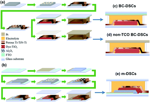
Scheme 1 illustrates the fabrication steps employed in this work for the preparation of back-contact dye-sensitized solar cells (denoted as BC-DSCs), non-TCO back-contact dye-sensitized solar cells (denoted as non-TCO BC-DSCs) and monolithic dye-sensitized solar cells (denoted as m-DSCs). As shown in Scheme 1(a), the TiO2 is screen-printed on FTO glass then polystyrene balls are dispersed on top of the sintered TiO2 layer by spin coating. A composite layer of Ti–TiN–Ti is sputtered to serve as a porous electron collecting electrode for both of the back contact device designs (BC-DSCs and non-TCO BC-DSCs). We first attempted to use a single TiN thin film as the back working electrode for device fabrication. However, it turned out that the TiN film would easily peel off from the TiO2 layer during ultrasonic bath treatment when rinsing off the polystyrene. Accordingly, the first Ti layer with a thickness of 250 nm was used as a buffer layer to prevent the TiN film from peeling off of the TiO2 layer. As for the second Ti layer with a thickness of 50 nm, it served as a protecting layer to prevent direct contact between the TiN film and the electrolyte, thus inhibiting charge recombination. Without the protecting Ti layer, the photocurrent decreased significantly mainly due to its ohmic contact behavior with the electrolyte. It is worth noticing that the overall thickness of the Ti–TiN–Ti film is constrained by the size of the polystyrene ball. When the overall thickness of the Ti–TiN–Ti composite film exceeds 500 nm (over half of the polystyrene ball diameter (800 nm)), it becomes difficult to remove the sealed polystyrene balls during the ultrasonic bath treatment. Fig. S1(a)† shows that over 50% of the polystyrene balls are left on the film after the removal process. This incomplete removal of the polystyrene balls would not only inhibit the infiltration of electrolyte but also reduce its diffusion pathway under working conditions. Eventually, we employed a tri-layer Ti–TiN–Ti thin film with a thickness of 400 nm as the charge collecting electrode with the aim of effective removal of the polystyrene balls, as revealed in Fig. S1(b).† Fig. S2(a)† depicts the cross-sectional transmission electron microscopy (TEM) image of the Ti–TiN–Ti film deposited on a glass substrate, which delivers a layer-by-layer sandwich configuration. Energy dispersive X-ray spectroscopy (EDX) mapping of the relevant elements N and Ti was conducted to confirm the composition as referred to in Fig. S2(b) and S2(c).† The process flow for the monolithic device is illustrated in Scheme 1(b), which shows that the FTO glass is platinized first and then the insulating spacer Al2O3 and mesoscopic TiO2 layer are sequentially screen-printed on the substrate. Fabrication of the Ti–TiN–Ti layer and the subsequent procedure then follows steps similar to those used for BC-DSCs except a plain glass is applied as the top sealing cover.Scheme 1(c)–(e) demonstrates the cross-sectional configurations of the BC-DSCs, non-TCO BC-DSCs and m-DSCs. For the non-TCO back contact device, a Pt foil was employed as the counter electrode rather than the FTO glass used for the BC-DSCs. As shown in Scheme 1(c) and (d), the photogenerated electrons injected into the mesoscopic semiconducting electrode (TiO2) would transport through the Ti–TiN–Ti electrode to be collected into an external circuit for both the BC-DSCs and non-TCO BC-DSCs. Meanwhile, the iodide/triiodide electrolyte infiltrates the mesoporous dye-covered TiO2 network through the porous Ti–TiN–Ti thin film to regenerate the dye cations and effectively transfer positive charge towards the counter electrode. The difference between BC-DSCs and m-DSCs is the path that positive charges diffuse through in the electrolyte. The direction in which positive charges transport in BC-DSCs is upwards through the counter electrode while, on the contrary, in m-DSCs the direction is downwards through the spacing layer (that is, the porous Al2O3 layer with a thickness of 200 nm) to the bottom platinized FTO glass. In other worlds, the carrier transport of the electrons and holes is in a parallel direction for BC-DSCs but in the opposite direction for m-DSCs.
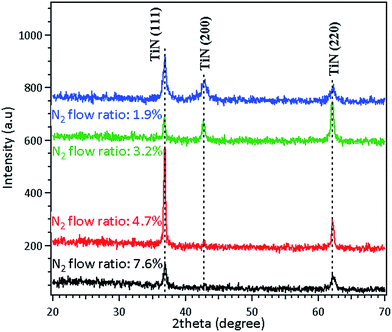
Fig. 1 displays the X-ray diffraction (XRD) patterns of the sputtered TiN thin film under different nitrogen flow ratios. The sheet resistances and film thicknesses of the sputtered TiN thin film under various nitrogen flow ratios are summarized in Table S1 in the ESI.† The XRD results confirm the crystal phases of TiN corresponding to the (111), (200) and (220) planes for these samples. Under a nitrogen flow ratio of 4.7% (N2![[thin space (1/6-em)]](https://www.rsc.org/images/entities/char_2009.gif) :
:![[thin space (1/6-em)]](https://www.rsc.org/images/entities/char_2009.gif) Ar = 1.5 sccm
Ar = 1.5 sccm![[thin space (1/6-em)]](https://www.rsc.org/images/entities/char_2009.gif) :
:![[thin space (1/6-em)]](https://www.rsc.org/images/entities/char_2009.gif) 30 sccm), the resultant film shows the best preferential crystal phase of plane (111). In addition, the sheet resistance of the TiN film (450 nm) was only 5.27 Ω per square under such doping conditions. Thus, the TiN layer used for the Ti–TiN–Ti thin film was fabricated under a nitrogen flow ratio of 4.7%. The influence of N2 doping on the deposited TiNX thin films by a reactive sputtering system has been investigated.26,27 It was found that TiN films with low sheet resistances have to be fabricated under appropriate nitrogen doping conditions in order to obtain the desired properties. Our results indicated that TiN films deposited under a nitrogen flow ratio of 4.7% were golden in color and exhibited better properties as shown in Table S1 (ESI†). According to the Drude model, the color of TiNX films can vary from metallic grey (mainly due to titanium metallic bonds) to gold and brownish red as the nitrogen flow increases.28 This is observed in our samples, as illustrated in Table S1.†
30 sccm), the resultant film shows the best preferential crystal phase of plane (111). In addition, the sheet resistance of the TiN film (450 nm) was only 5.27 Ω per square under such doping conditions. Thus, the TiN layer used for the Ti–TiN–Ti thin film was fabricated under a nitrogen flow ratio of 4.7%. The influence of N2 doping on the deposited TiNX thin films by a reactive sputtering system has been investigated.26,27 It was found that TiN films with low sheet resistances have to be fabricated under appropriate nitrogen doping conditions in order to obtain the desired properties. Our results indicated that TiN films deposited under a nitrogen flow ratio of 4.7% were golden in color and exhibited better properties as shown in Table S1 (ESI†). According to the Drude model, the color of TiNX films can vary from metallic grey (mainly due to titanium metallic bonds) to gold and brownish red as the nitrogen flow increases.28 This is observed in our samples, as illustrated in Table S1.†
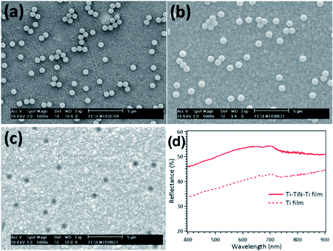
The morphologies of the polystyrene balls spun on the TiO2 layer and after deposition of the Ti–TiN–Ti electrode are shown in the scanning electron microscopy (SEM) images presented in Fig. 2(a) and (b). The influence of the concentration of the polystyrene solution on the pore distribution was investigated (see Fig. S3 in the ESI†). Here, we used a diluted polystyrene solution in ethanol with a volume ratio of 1![[thin space (1/6-em)]](https://www.rsc.org/images/entities/char_2009.gif) :
:![[thin space (1/6-em)]](https://www.rsc.org/images/entities/char_2009.gif) 199. The SEM image of the porous Ti–TiN–Ti electrode after removal of the polystyrene balls is shown in Fig. 2(c). It can be seen in Fig. 2(c) that the polystyrene balls are separated by distances of several micrometers without severe aggregation. This distance is of a similar scale to electrolyte transport in conventional DSCs in which the spacer between the two FTO glasses is around a few tens of micrometers. This allowed the positive charges beneath the porous electrode to transport laterally in order to find the pores for travelling towards the counter electrode without increasing the resistivity too much. Fig. 2(d) presents the reflectance spectra of Ti–TiN–Ti and Ti thin films with comparable film thickness. A reflectance that was enhanced by more than 10% was observed for the Ti–TiN–Ti film over that of the Ti film in the wavelength range of between 400 nm to 700 nm, which almost covers the region of dye absorption for extension of the optical path. This result further confirms the advantage, in terms of light harvesting, of employing a Ti–TiN–Ti thin film as the electrode rather than a Ti film.
199. The SEM image of the porous Ti–TiN–Ti electrode after removal of the polystyrene balls is shown in Fig. 2(c). It can be seen in Fig. 2(c) that the polystyrene balls are separated by distances of several micrometers without severe aggregation. This distance is of a similar scale to electrolyte transport in conventional DSCs in which the spacer between the two FTO glasses is around a few tens of micrometers. This allowed the positive charges beneath the porous electrode to transport laterally in order to find the pores for travelling towards the counter electrode without increasing the resistivity too much. Fig. 2(d) presents the reflectance spectra of Ti–TiN–Ti and Ti thin films with comparable film thickness. A reflectance that was enhanced by more than 10% was observed for the Ti–TiN–Ti film over that of the Ti film in the wavelength range of between 400 nm to 700 nm, which almost covers the region of dye absorption for extension of the optical path. This result further confirms the advantage, in terms of light harvesting, of employing a Ti–TiN–Ti thin film as the electrode rather than a Ti film.
The interface junction behavior between the porous electrode and the electrolyte is of critical importance for the operation of DSC devices. As reported in previous work, the interface has been confirmed to represent a Schottky contact between the Ti electrode and the I−/I3− electrolyte.9 Therefore, we tested symmetric dummy cells that employed different materials in order to examine the interfacial contact behavior (Fig. 3). It is apparent that symmetrically rectified curves were measured for these dummy cells, thus implying that Schottky contact formed on these interfaces. The results show that both TiN and Ti–TiN–Ti, like FTO, can act as WE materials. Since the devices were not fabricated with the same thicknesses for TiN and Ti–TiN–Ti, they showed different series resistances.
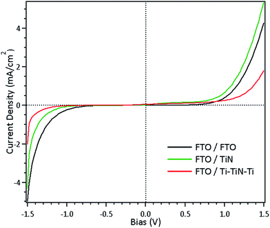 | ||
| Fig. 3 J–V characteristic curves of dummy cells fabricated using FTO, and glass substrates deposited with sputtered TiN film, and sputtered Ti–TiN–Ti film as counter electrodes. | ||
Table 1 summarizes the photovoltaic performances of BC-DSCs, non-TCO BC-DSCs and monolithic DSCs compared with those of conventional sandwiched DSCs sensitized with Z-907 dye and MK-2 dye with TiO2 layers of similar thickness. The complete photovoltaic parameters of the BC-DSCs sensitized with both dyes using various TiO2 film thicknesses are summarized in Table S2 (ESI†). The current–voltage characteristics and IPCE spectra for the back contact devices are listed in Table 1 and displayed in Fig. 4. In comparison with Ref-DSCs, BC-DSCs sensitized with Z-907 and MK-2 delivered comparable open-circuit voltages (VOC) of 720 mV and 740 mV and yielded overall conversion efficiencies of 4.53% and 4.16%, which are 65.1% and 65.8% of those of their respective Ref-DSC counterparts. On the other hand, BC-DSCs sensitized with both dyes generated relatively lower short-circuit current densities (JSC), 9.06 mA cm−2 and 7.88 mA cm−2, than those of the Ref-DSCs. When comparing all of the photovoltaic parameters of the BC-DSCs with those of the Ref-DSCs, it becomes obvious that the short-circuit current density is the major element responsible for the lower device efficiencies. The variation in photocurrent density between the BC-DSCs and Ref-DSCs is almost proportional to the difference between the device efficiencies. It is speculated that this is due to two main reasons. First, electrons transporting on a porous Ti–TiN–Ti electrode might suffer more recombination losses than on an FTO substrate as the area exposed to the electrolyte is enlarged, which leads to a decreased photocurrent density. The slightly higher resistance of the Ti–TiN–Ti electrode in comparison with that of the FTO substrate might decrease the charge collection. Second, the charge generation distribution profile is not favorable for BC-DSCs.29 Previous results have shown that the wavelength dependence of the electron generation rate within the TiO2 layer impacts the charge collection significantly. The concentration of photo-generated carriers induced from high-energy photons (where dyes have large absorption coefficients) would be attenuated sharply on the illuminated side and thus the charge generation rate would decrease rapidly across the TiO2 film. For example, the electrons generated under an incident light wavelength of 540 nm in conventional DSCs can easily reach the FTO conductive electrode while, on the contrary, those in BC-DSCs have to travel a longer distance to reach the porous Ti–TiN–Ti electrode located on the opposite side of the illumination. Consequently, more recombination losses occur during electron transportation in BC-DSCs. This phenomenon is profoundly demonstrated in the thickness dependent IPCE values using two dyes with different absorption coefficients, as shown in Fig. 4(c) and (d). Electrons have to travel a longer distance to the Ti–TiN–Ti electrode in BC-DSCs sensitized with MK-2 since the electron generation rate decreases more rapidly due to its higher molar extinction coefficient. Thus, the IPCE values in the visible range for the BC-DSCs sensitized with MK-2 exhibit minor variation upon increasing the TiO2 film thickness because of the high molar extinction coefficient of MK-2. On the other hand, the IPCE values for BC-DSCs sensitized with Z-907 demonstrate obvious enhancement in the short wavelength visible region. The IPCE values for the BC-DSCs sensitized with both dyes demonstrate similar increases in the infrared region, which means that electrons irradiated under wavelengths in the infrared region can effectively transport to the Ti–TiN–Ti electrode. Meanwhile, according to the effect of the dye molar extinction coefficient, the BC-DSC sensitized with Z-907, which has a lower molar extinction coefficient, exhibited a higher photocurrent density and power conversion efficiency when a thicker TiO2 film was used. The dependence of the short-circuit current density and power conversion efficiencies on the TiO2 film thickness is shown in Fig. S4 in the ESI.† An optimized JSC and efficiency of the BC-DSCs sensitized with MK-2 is achieved when the TiO2 film thickness is around 9 μm, while that of the BC-DSCs sensitized with Z-907 is around 11 μm. Within the constraints of the thickness of the Ti–TiN–Ti electrode, we further reduced the electrode thickness in order to observe the impact of electrode thickness on the BC-DSC’s performances. As mentioned above, 250 nm and 50 nm-thick Ti layers are necessary for the first and third layer depositions in order to prevent the electrode film from peeling off during the ultrasonic bath treatment and ohmic contact with the electrolyte. The thickness of TiN was reduced from 100 nm to 50 nm in order to achieve an overall Ti–TiN–Ti thickness of 350 nm. The corresponding J–V photovoltaic parameters of the BC-DSCs with Z-907 and MK-2 are given in Table S3.† Compared with the results of the BC-DSCs with a porous electrode thickness of 400 nm, the device efficiencies are lower in terms of decreased JSC and FF values due to the lower conductivity of the reduced thickness TiN layer.
| TiO2 thickness (μm) | V OC (mV) | J SC (mA cm−2) | FF | PCE (%) | PCE relative to reference DSCs | |
|---|---|---|---|---|---|---|
| Ref-DSCs Z-907 | 10.6 | 695 | 14.64 | 0.67 | 6.96 | |
| BC-DSCs Z-907 | 10.6 | 720 | 9.06 | 0.69 | 4.53 | 65.1% |
| Non-TCO BC-DSCs Z-907 | 10.6 | 721 | 7.6 | 0.64 | 3.53 | 50.7% |
| m-DSCs Z-907 | 10.6 | 632 | 8.0 | 0.62 | 3.16 | 45.4% |
| Ref-DSCs MK-2 | 8.8 | 703 | 12.96 | 0.69 | 6.32 | |
| BC-DSCs MK-2 | 8.8 | 740 | 7.88 | 0.71 | 4.16 | 65.8% |
| Non-TCO BC-DSCs MK-2 | 8.8 | 736 | 5.87 | 0.69 | 2.99 | 47.3% |
| m-DSCs MK-2 | 8.8 | 664 | 6.46 | 0.68 | 2.92 | 46.2% |
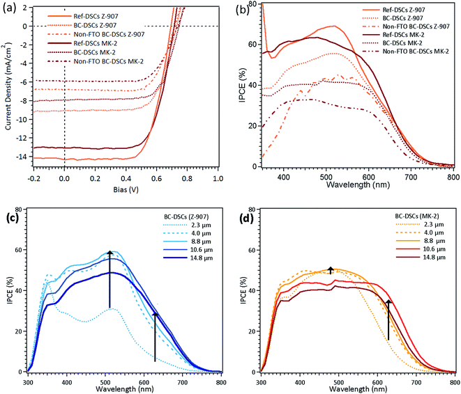 | ||
| Fig. 4 The (a) J–V and (b) IPCE characteristic curves of the devices listed in Table 1. IPCE curves of BC-DSCs with different thickness TiO2 layers sensitized with (c) Z-907 dye and (d) MK-2 dye. | ||
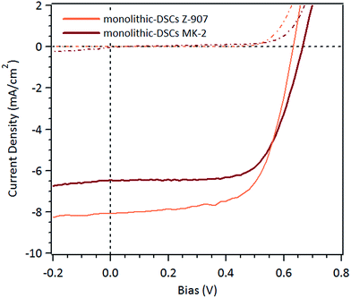
The photovoltaic performances of m-DSCs employing porous Ti–TiN–Ti electrodes are listed in Table 1 and their current–voltage characteristics presented in Fig. 5 in order to compare their performances with those of the BC-DSCs and Ref-DSCs. The PCEs of the m-DSCs, 3.16% (Z-907) and 2.92% (MK-2), were lower in comparison with those of the BC-DSCs mainly due to the loss in voltage. This is probably due to the reduced contact area between the platinized-FTO and the electrolyte which leads to an increased resistance of charge transfer at the counter electrode. Another effect is that the carriers in this configuration travelling in anti-parallel directions inside the mesoscopic sensitized layer can lead to a higher potential for charge recombination.
Conclusion
In summary, we have successfully proposed a novel method to fabricate a porous Ti–TiN–Ti thin film as an electrode material for three novel devices, namely back-contact DSCs (BC-DSCs), non-TCO back-contact DSCs and monolithic DSCs. The dependence of the photocurrent density and device efficiencies of the BC-DSCs on the TiO2 film thickness was examined. The BC-DSC sensitized with Z-907 yielded a power conversion efficiency of 4.53% and the one sensitized with MK-2 yielded a device efficiency of 4.16%, which are both around two thirds of the PCE value obtained from conventional sandwiched DSC architectures. The device performances of non-TCO back-contact DSCs and monolithic DSCs applying porous Ti–TiN–Ti electrodes were around half that of standard conventional DSCs.Acknowledgements
P. C. appreciates the research funding from the Minister of Science and Technology (MOST) of Taiwan (MOST 103-2221-E-006-029-MY3) and the financial support from the Top-Notch Project under the Headquarters of University Advancement at National Cheng Kung University, which is sponsored by the Ministry of Education, Taiwan, ROC.References
- B. O’Regan and M. Gratzel, Nature, 1991, 353, 737–740 CrossRef.
- A. Yella, H.-W. Lee, H. N. Tsao, C. Yi, A. K. Chandiran, M. K. Nazeeruddin, E. W.-G. Diau, C.-Y. Yeh, S. M. Zakeeruddin and M. Grätzel, Science, 2011, 334, 629–634 CrossRef CAS PubMed.
- S. Mathew, A. Yella, P. Gao, R. Humphry-Baker, F. E. CurchodBasile, N. Ashari-Astani, I. Tavernelli, U. Rothlisberger, K. NazeeruddinMd and M. Grätzel, Nat. Chem., 2014, 6, 242–247 CrossRef CAS PubMed.
- K. Kakiage, Y. Aoyama, T. Yano, K. Oya, J.-i. Fujisawa and M. Hanaya, Chem. Commun., 2015, 51, 15894–15897 RSC.
- S. Ito, T. N. Murakami, P. Comte, P. Liska, C. Grätzel, M. K. Nazeeruddin and M. Grätzel, Thin Solid Films, 2008, 516, 4613–4619 CrossRef CAS.
- J. M. Kroon, N. J. Bakker, H. J. P. Smit, P. Liska, K. R. Thampi, P. Wang, S. M. Zakeeruddin, M. Grätzel, A. Hinsch, S. Hore, U. Würfel, R. Sastrawan, J. R. Durrant, E. Palomares, H. Pettersson, T. Gruszecki, J. Walter, K. Skupien and G. E. Tulloch, Prog. Photovoltaics, 2007, 15, 1–18 CAS.
- F. Nobuhiro, F. Atsushi, C. Yasuo, K. Ryoichi, Y. Ryosuke and H. Liyuan, Jpn. J. Appl. Phys., 2007, 46, L420 CrossRef.
- N. Fuke, A. Fukui, R. Komiya, A. Islam, Y. Chiba, M. Yanagida, R. Yamanaka and L. Han, Chem. Mater., 2008, 20, 4974–4979 CrossRef CAS.
- N. Fuke, A. Fukui, A. Islam, R. Komiya, R. Yamanaka, H. Harima and L. Han, Sol. Energy Mater. Sol. Cells, 2009, 93, 720–724 CrossRef CAS.
- Y. Kashiwa, Y. Yoshida and S. Hayase, Appl. Phys. Lett., 2008, 92, 033308 CrossRef.
- N. Fuke, R. Katoh, A. Islam, M. Kasuya, A. Furube, A. Fukui, Y. Chiba, R. Komiya, R. Yamanaka, L. Han and H. Harima, Energy Environ. Sci., 2009, 2, 1205–1209 Search PubMed.
- N. Tjitra Salim, K. Zhang, S. Zhang and L. Han, Appl. Phys. Lett., 2012, 101, 233905 CrossRef.
- D. Fu, X. L. Zhang, R. L. Barber and U. Bach, Adv. Mater., 2010, 22, 4270–4274 CrossRef CAS PubMed.
- H. Yang, D. Fu, M. Jiang, J. Duan, F. Zhang, X. Zeng and U. Bach, Thin Solid Films, 2013, 531, 519–524 CrossRef CAS.
- D. Fu, P. Lay and U. Bach, Energy Environ. Sci., 2013, 6, 824–829 CAS.
- M. Z. Molla, N. Mizukoshi, H. Furukawa, Y. Ogomi, S. S. Pandey, T. Ma and S. Hayase, Prog. Photovoltaics, 2015, 23, 1100–1109 CAS.
- M. Z. Molla, M. Kawano, A. K. Baranwal, S. S. Pandey, Y. Ogomi, T. Ma and S. Hayase, RSC Adv., 2016, 6, 33353–33360 RSC.
- F.-Y. Ouyang and W.-L. Tai, Appl. Surf. Sci., 2013, 276, 563–570 CrossRef CAS.
- B. Yoo, K.-J. Kim, Y. H. Kim, K. Kim, M. J. Ko, W. M. Kim and N.-G. Park, J. Mater. Chem., 2011, 21, 3077–3084 RSC.
- G. R. Li, F. Wang, J. Song, F. Y. Xiong and X. P. Gao, Electrochim. Acta, 2012, 65, 216–220 CrossRef CAS.
- H. Xu, X. Zhang, C. Zhang, Z. Liu, X. Zhou, S. Pang, X. Chen, S. Dong, Z. Zhang, L. Zhang, P. Han, X. Wang and G. Cui, ACS Appl. Mater. Interfaces, 2012, 4, 1087–1092 CAS.
- Q. W. Jiang, G. R. Li and X. P. Gao, Chem. Commun., 2009, 44, 6720–6722 RSC.
- X. Zhang, X. Chen, S. Dong, Z. Liu, X. Zhou, J. Yao, S. Pang, H. Xu, Z. Zhang, L. Li and G. Cui, J. Mater. Chem., 2012, 22, 6067–6071 RSC.
- K. Yoo, J.-Y. Kim, J. A. Lee, J. S. Kim, D.-K. Lee, K. Kim, J. Y. Kim, B. Kim, H. Kim, W. M. Kim, J. H. Kim and M. J. Ko, ACS Nano, 2015, 9, 3760–3771 CrossRef CAS PubMed.
- Y. Nishio, T. Yamaguchi, T. Yamguchi, K. Nishio and S. Hayase, J. Appl. Electrochem., 2016, 46, 551–557 CrossRef CAS.
- Q. Fang and J. Y. Zhang, Int. J. Inorg. Mater., 2001, 3, 1193–1196 CrossRef CAS.
- S. Mahieu and D. Depla, J. Phys. D: Appl. Phys., 2009, 42, 053002 CrossRef.
- P. Roquiny, F. Bodart and G. Terwagne, Surf. Coat. Technol., 1999, 116–119, 278–283 CrossRef CAS.
- N. Fuke, A. Fukui, A. Islam, R. Komiya, R. Yamanaka, L. Han and H. Harima, J. Appl. Phys., 2008, 104, 064307 CrossRef.
Footnote |
| † Electronic supplementary information (ESI) available. See DOI: 10.1039/c6se00118a |
| This journal is © The Royal Society of Chemistry 2017 |

