 Open Access Article
Evidence of enhanced photocurrent response in corannulene films†
N. Pastukhovaa,
L. Martin Samosbc,
L. Zoppid,
E. Pavlica a,
J. Mathewa,
G. Bratina
 a,
J. S. Siegel
 e and
K. K. Baldridge
 *e
*e
aLaboratory of Organic Matter Physics, University of Nova Gorica, Vipavska 13, SI-5000 Nova Gorica, Slovenia
bMaterial Research Laboratory, University of Nova Gorica, Vipavska 13, SI-5000 Nova Gorica, Slovenia
cCNR-IOM DEMOCRITOS, Istituto Officina dei Materiali, c/o SISSA Scuola Internazionale Superiore di Studi Avanzati, Via Bonomea 265, 34136 Trieste, Italy
dDepartment of Chemistry, University of Zürich, Winterthurerstrasse 190, CH-8057, Zürich, Switzerland
eSchool of Pharmaceutical Science and Technology, Tianjin University, 92 Weijin Road, Nankai District, Tianjin, 300072, P. R. China. E-mail: kimb@tju.edu.cn
First published on 25th September 2017
Abstract
Photoconductivity spectra measured in non-crystalline corannulene thin layers are compared to optical absorption in solution phase and thin films. The unexpected enhanced photoconductivity is correlated with GW–BSE theoretical predictions of corannulene gas-phase excitonic spectra. Theoretical analysis reveals a consistent contribution involving transitions to Super Atomic Molecular Orbitals (SAMOs), a unique set of diffuse orbitals typical of curved conjugated constructs. Results suggest SAMO population via direct photoexcitation as a potential mechanism towards exploiting these diffuse orbitals as conducting channels in suitably assembled quantum nanostructures or solids.
Introduction
Carbon allotropes have been found to exhibit interesting optoelectronic properties, including high carrier mobility and broad spectral absorption, most prominently graphene1 or the strong electronic accepting ability in fullerenes.2 Renewed interest in the use of π-conjugated molecules as components in nanoscale electronics has motivated recent efforts to control and optimize charge transport at the molecular scale.3–5 When molecular units are assembled in quantum nanostructures or solids, intermolecular electronic wave functions overlap and the consequent band formation becomes strategic towards enhancement of charge transfer/transport properties in the molecular material.6–8An alternate mechanism of intermolecular charge transport distinct from conventional mechanisms involving tightly bound π molecular orbital overlap, has been identified in curved and hollow aromatic molecules and is of particular interest for exploitation in materials.9–11 Key to this type of electron transport mechanism is evidence of a characteristic set of diffuse molecular orbitals, called Super Atomic Molecular Orbitals, SAMOs,9 universally existent in curved and hollow shaped molecules10,12–14 and first investigated in low-temperature scanning tunneling microscopy experiments (LT-STM) for the case of C60.9
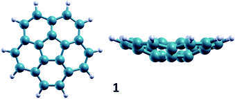
Curved polynuclear aromatic hydrocarbons (PAH), such as the smallest bowl structure corannulene, 1 (Fig. 1), with tunable electrical and optical band gaps, offer attractive alternatives to graphene nanoparticles or fullerenes.15,16 Much effort has been extended towards design of functionalized building blocks based on this fragment, focusing on tailoring electronic properties such as electrical and optical band gaps.16 Assembled in the solid state, functionalized bowl fragments have led to an array of materials supported in varying complex environments, which can be exploited as active molecular layers in optoelectronic applications,17,18 aggregated as monolayers on metallic surfaces for work-function engineering,19 and, as single molecules in junctions for transport processes.20 Moreover, the large electron-acceptor ability of 1, which normalized per C atom goes beyond that of C60,21 and the possibility of changing its packing mode in the solid state to columnar packing through chemical functionalization16 is expected to offer a more efficient transport mechanism than C60.
The detailed investigation of electron transport properties in these bowl-shaped derived materials provides a powerful template for improving our knowledge of electronic transport phenomena, which, in turn, has the potential to lead to advancements in experimental measurement capabilities as well as in the fundamental theoretical understanding of their construction.
To this aim, the strategy adopted in the present work combines time of flight (TOF)22 photoconductivity experiments performed on thin layers of 1 and optical absorption in solution phase and thin films with theoretical predictions (GW–BSE)23 of excitonic properties of 1 in the gas phase.
In a typical photoconductivity experiment, photon–molecule interactions result in photogenerated charge carriers that reach the electrodes under the effect of an external applied electric field. Specific to the present time-of-flight (TOF) approach,22 which is a variant of a transient photoconductivity method,24 the resulting photocurrent persists until all photo-excited carriers reach the electrode, recombine, or thermodynamically relax to localized electronic states. Therefore, the amount of collected carriers on the electrode is a clear measure of the existence of transporting channels.22
Most notably, photocurrent as a function of photon energy yields information concerning the excitation energies at which high-mobility pathways are activated. In this regard, the optical absorption together with corresponding theoretical analysis of the excitonic structure is fundamental towards establishing the connection between the photo-activated transport channels and the nature of the orbitals involved in the transport process. Based on the present results, it is asserted that population of SAMOs, as induced by direct photoexcitation, offers a potential as a strategy towards exploiting such types of diffuse orbitals as conducting channels in suitably assembled quantum nanostructures or solids.
Experimental and theoretical methodologies
Solution absorption studies
Stock solutions of 1 (ca. 0.1 M) were prepared, with assistance of sonication in spectral grade solvents, which included chloroform (CF), dichloromethane (DCM), and diethyl ether (DEE), diluted serially (ca. 0.002 M). The UV/visible absorption spectra of these solutions in 10 mm quartz cuvettes (Hellma 114-QS) were measured (Perkin Elmer Lambda 650S); each spectrum is an average of 3 repetitions to reduce noise to signal ratio. Blank solvents were measured to eliminate background.Thin film preparation and characterization
Corannulene films were prepared by heating a solution (0.023 M in CF) to 40 °C for 10 min then immediate spin-coating of 60 μl of solution on a quartz substrate (1 cm × 1 cm) at 1500 rpm for 60 s (acceleration ca. 10![[thin space (1/6-em)]](https://www.rsc.org/images/entities/char_2009.gif) 000 rpm s−1) in a nitrogen-filled glovebox at room temperature ([H20] and [O2] < 10 ppm). In order to improve surface coverage, spin-coating was repeated once over the first layer with exactly the same parameters. The second coating had no influence on the results. Topographic images of spin-coated layers were obtained with an Atomic Force Microscope (A.P.E. Research) operating in non-contact mode. Optical absorption measurements of spin-coated films were carried out using the spectrophotometer Perkin Elmer Lambda 650S. Absorption of a clean quartz substrate was subtracted from the absorption of corannulene-covered quartz. Absorption spectra of single and double spin-coated samples exhibit equal peak positions, but varying magnitude, commensurate with the thickness variation.
000 rpm s−1) in a nitrogen-filled glovebox at room temperature ([H20] and [O2] < 10 ppm). In order to improve surface coverage, spin-coating was repeated once over the first layer with exactly the same parameters. The second coating had no influence on the results. Topographic images of spin-coated layers were obtained with an Atomic Force Microscope (A.P.E. Research) operating in non-contact mode. Optical absorption measurements of spin-coated films were carried out using the spectrophotometer Perkin Elmer Lambda 650S. Absorption of a clean quartz substrate was subtracted from the absorption of corannulene-covered quartz. Absorption spectra of single and double spin-coated samples exhibit equal peak positions, but varying magnitude, commensurate with the thickness variation.
Time-of-flight (TOF) photoconductivity measurements
TOF photoconductivity methodology22 was used to measure the photoconductivity of spin-coated layers of 1. Two coplanar 100 nm thick Au electrodes were vacuum-deposited through shadow mask onto the quartz substrate (interelectrode distance 50–200 μm) prior to spin-coating (Scheme 1).22,25–28 TOF measurements were performed by applying DC voltage (Vb) ranging from −500 V to 500 V between electrodes. The biased electrode was connected also to a current amplifier through a bias-t element (particulars BT-01), which is used to decouple transient photocurrent response from the constant dark current, schematically depicted as capacitor (C) and inductor (L) in Scheme 1.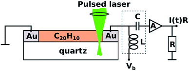 | ||
| Scheme 1 View of the time-of-flight photoconductivity measurement apparatus with a coplanar electrode setup and corannulene on quartz substrate. | ||
Charge carriers were generated using a pulsed laser (3 ns duration; 10 Hz repetition rate) of a tunable photon energy between 3.5 eV (350 nm) and 5.9 eV (210 nm). The laser light was focused near the biased electrode in the direction normal to the sample surface. Laser pulse intensity was attenuated to ensure that the total charge (the time integral of the photocurrent pulse) was less than 10% of the total capacitor charge and hence the photogenerated charge could not screen the external electric field. The photocurrent transients I(t) were amplified by a 2 GHz current amplifier (particulars AM-01A) and recorded by a 2.5 GHz oscilloscope (Lecroy, WavePro 725i). Au electrodes were connected to bias-t and current amplifier by 4 GHz probe tips (Signatone SP-100). Sample preparation and all measurements were performed in a nitrogen-filled glovebox at room temperature with H2O and O2 concentration below 10 ppm.
Computational methodology
In the present work, a customized hybrid methodology is exploited, using standard quantum chemical techniques (B97D/Def2-TZVPP29) as implemented in the GAMESS30 for full optimization and Hessian characterization of structures, followed by plane-wave DFT formalism (Quantum-ESPRESSO)31 within the MBPT23 in the GW32,33–BSE23 approach (SAX).34 Initialization of the GW calculation for the fully optimized molecular structure occurs from a DFT-PZ35 electronic structure calculation at the Γ point, with a 45 Ry energy cut-off for the electronic wave function. Within the GW approximation,23,32,33 the self-energy is calculated as the product of a single-particle Green function, G, and a nonlocal and dynamically screened Coulomb potential, W, (Σ = iGW). For the evaluation of the polarizability, a 2 Ry energy cut-off and 1024 electronic bands have been used, using a Godby–Needs plasmon pole approximation36 for the energy dependence of the screened Coulomb potential. Studies have established non self-consistent GW, namely G0W0,37 to enable highly accurate predictions with respect to experiment, substantiating the use of this theory as a standard approach for practical calculations. Accurate description of electronic excitations are achieved by solving the Bethe–Salpeter equation (BSE)23 within the Tamm–Dancoff approximation.38 Within this formalism, neutral excitation energies and optical spectra are obtained from the solution of an effective two-particle Hamiltonian, which, using the GW data, accounting for screened electron–hole interactions.Results and discussion
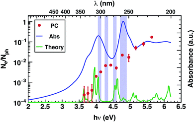
The photoconductivity (EQE) of corannulene layers (red dots) versus photon energy and the optical absorption spectrum of 1 thin film (solid line) are shown in Fig. 2. The EQE is negligible for excitation energies below 4.0 eV, displaying a low signal to noise ratio for energies between 3.6 and 3.9 eV. At 4.0 eV, the photocurrent starts to rise and exhibits up to one order of magnitude increase at 4.4 eV. Interestingly, this first photocurrent peak is manifesting over an energy region where the optical absorption is decreasing (4.0–4.5 eV). Moreover, the EQE does not exhibit any further decay over the range of the measured wavelengths.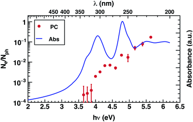 | ||
| Fig. 2 Photoconductivity (PC – red symbols) and optical absorption (Abs – blue line) of corannulene thin layer. | ||
Since EQE is the product of absorption as photon-to-charge conversion efficiency and mobility,39 the peak at 4.4 eV represents a significant increase of mobility and/or charge extraction efficiency. Samples used for transient photoconductivity measurements exhibited disordered surfaces comprising approximately 80 nm high, 0.4 μm wide, and 5 μm long structures, randomly distributed along the layer (see ESI Fig. S4†). In the absence of experimental information of eventual ordering of the molecules within the layer, one can surmise that the elongated structures include some kind of ordered assemblies of 1, most likely formed via van der Waals interactions. One expects that charge transport in ordered regions, which may involve overlap between orbitals in adjacent molecules, to be faster relative to the disordered regions of the layer.
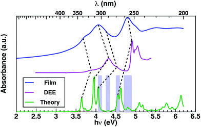
In order to provide an interpretation on the nature of the orbitals possibly contributing to the transporting channels, it is fundamental to link the EQE and the measured absorption spectrum through the theoretical analysis of the excitonic structure.40 This is established considering the GW–BSE theoretical predictions of excitonic properties of 1 in gas phase, which enables more detail into the photo-excited channels potentially available for charge transport. Measured absorption spectra in thin layer 1 and in diethyl-ether (DEE) solution, together with the GW–BSE calculated gas-phase optical absorption spectrum for 1 are shown in Fig. 3.
Theoretical predictions for each optical excitation (green line in Fig. 3) enable one to disentangle the molecular states to which the charge carriers are excited. Moreover, it is possible to identify specific combinations of orbitals that dominate over others. Such analyses facilitate interpretation of the experimental spectra by identification of specific orbital contributions. In particular, the optical transitions associated to the low-energy excitations predominantly involve the frontier molecular orbitals. The first two peaks at 3.6 and 3.7 eV are ∼62–64% HOMO-to-LUMO transitions, and the 3rd peak at 3.9 eV is ∼45% (HOMO-1)-to-LUMO transition. The SAMO contribution comes in at 4.1 eV (Table 1), with a very small peak at 4.3 eV having the highest transition probability with ∼57% contribution from a HOMO-to-SAMO transition. The energy of these excitations is well below the transport gap calculated at 7.1 eV, indicating that these transitions involve tightly bound excitons.
| Spectral region | Energy range (eV) | Initiating orbital | Transitioning orbital | Contribution |
|---|---|---|---|---|
| A | 4.05–4.15 | HOMO | SAMO s | 30% |
| B | 4.25–4.35 | HOMO | SAMO s | 60% |
| C | 4.5–4.6 | HOMO | SAMO s | 20% |
| D | 4.7–4.9 | HOMO | SAMO p | 40% |
| SAMO d | 20% |
The experimental spectra measured in dilute solutions (magenta line Fig. 3) exhibit good agreement with the theoretical spectra modulo a typical solvent shift of ∼0.35 eV,41 suggesting relatively weak interaction of 1 with the solvent. The first four lowest-energy peaks of the theoretical spectrum can be correlated to the first four experimental peaks, at energies of 3.9 eV, 4.1 eV, 4.3 eV, and 4.5 eV, respectively, as determined via Gaussian fitting (for details see ESI†). Theoretical excitation at 4.6 eV exhibits good agreement with the absorption peak at 4.95 eV.
The absorption in a thin layer (blue line Fig. 3) exhibits broad peaks centered at 4.0 eV and 4.8 eV, which correspond to the two groups of peaks (3.6–4.7 eV/4.7–5.0 eV) observed in the solution spectrum (magenta curve). The peaks observed in thin layer 1 at energies 3.7 eV and 4.1 eV appear in the solution spectrum (magenta line Fig. 3) blue-shifted by ∼0.2–0.3 eV, while the highest energy excitation at 4.8 eV is blue-shifted by only 0.1 eV in solution.
Throughout the energy range between the absorption edge (3.5 eV) and the highest energy excitation (5.5 eV), it is possible to establish a correspondence between the main features of the measured absorption spectra of thin layer and solution, as indicated by dashed lines in Fig. 3. Notably, there is saddle region of the experimental thin-film spectrum between 4.2 eV and 4.6 eV that appears not to be associated with any contribution from conventional molecular transitions, but which aligns with the theoretical predictions associated with a SAMO s orbital arising at ∼4.3 eV in the optical absorption (Table 1 and Fig. 3 violet boxes).
Most importantly, comparison between the photocurrent, the absorption of a thin film, and theoretical predictions (Fig. 4), reveals an enhancement in the photocurrent over the same energy region (4.2 eV–4.6 eV) where excitations are predicted to occur between molecular orbitals and SAMO states (Fig. 4, violet boxes). Based on these results, we speculate that transport mediated by SAMO states could be a possible interpretation to account for the enhanced photocurrent in corannulene films. In fact, as opposed to the more traditional mechanism of intermolecular electron transport, the paradigm for the intermolecular orbital hybridization and potential for charge transport exploiting the diffuse nature of the SAMOs, would provide a much more efficient path than that involving the more tightly bound π molecular orbitals associated to aromatic molecules.11
Nevertheless, it should be emphasized that electron transport as mediated through SAMO hopping has not been exclusively established in experiments as of yet. To the extent that Frontier orbitals participate in charge-transport applications, to be relevant for molecular transport, the SAMO derived states would need to be either the 1st unoccupied state, or, should cross the Fermi level of the material, thereby enhancing the possibility for their occupation.11,15 In this respect, molecular engineering has proven to be a powerful tool for enabling more focused control of the relative energy positioning (gap) of the LUMO and SAMO of lowest energy (i.e., ΔESAMO–LUMO). The tailoring of designed molecular components with more optimal positioning of SAMO-type orbitals with respect to the conventional molecular LUMO, has the potential for inducement of SAMO-mediated electron transport.11,15,42
Towards this end, theoretical GW predictions of SAMO energies in 1 already have revealed a ΔESAMO–LUMO energy gap nearly one order of magnitude lower than that found in C60 (calc. 0.3 eV vs. 2.4 eV).42 This suggests an avenue towards design of tailored bowl fragments, which drive the SAMO orbitals down below the LUMO, and provide suitable candidates for further investigation of SAMO-mediated molecular transport enabled materials through experimental techniques of the type established in the present work.
Conclusions
Photoconductivity experiments in non-crystalline corannulene thin layers and optical absorption in solution phase and thin films are used in conjunction with theoretical GW–BSE predictions of excitonic structure, for better understanding of orbital induced electron transport through SAMO junctions. The rise in the photocurrent over energy regions where the optical absorptivity profile is decreasing correlates well with the regions where diffuse Super Atomic Molecular Orbitals (SAMO) are predicted to contribute. Results suggest that SAMOs population via direct photoexcitation could represent a strategy towards exploitation of such diffuse orbitals as conducting channels in suitably assembled quantum nanostructures or solids.Conflicts of interest
There are no conflicts to declare.Acknowledgements
L. Z. gratefully acknowledges the University of Zurich, URPP LightChEC program, and the CSCS supercomputing center for a grant of computer time. K. K. B and J. S. S. acknowledge the National Basic Research Program of China (2015CB856500), the Qian Ren Scholar Program of China, and the Synergistic Innovation Center of chemical Science and Engineering (Tianjin) for support of this work. L. M.-S. acknowledges the Slovenian Research Agency. J. M. acknowledges support of the Slovenian Research Agency under the Young researchers program. This work was funded in part by Slovenian Research Agency through the research program P1-0055. N. P. acknowledges the Slovene Human Resources Development and Scholarship Fund. We acknowledge Matjaz Valant for his advice and support.References
- K. S. Novoselov, V. I. Fal'ko, L. Colombo, P. R. Gellert, M. G. Schwab and K. Kim, Nature, 2012, 490, 192 CrossRef CAS PubMed.
- A. J. Ferguson, J. L. Blackburn and N. Kopidakis, Mater. Lett., 2012, 90, 115 CrossRef.
- H. Song, M. A. Reed and T. Lee, Adv. Mater., 2011, 23, 1583 CrossRef CAS PubMed.
- S. V. Aradhya and L. Venkataraman, Nat. Nanotechnol., 2013, 8, 399 CrossRef CAS PubMed.
- C. M. Guédon, H. Valkenier, T. Markussen, K. S. Thygesen, J. C. Hummelen and S. J. v. d. Molen, Nat. Nanotechnol., 2012, 7, 305 CrossRef PubMed.
- R. Temirov, S. Soubatch, A. Luican and F. S. Tautz, Nature, 2006, 444, 350 CrossRef CAS PubMed.
- N. Gonzalez-Lakunza, I. Fernández-Torrente, K. J. Franke, N. Lorente, A. Arnau and J. I. Pascual, Phys. Rev. Lett., 2008, 100, 256805 CrossRef PubMed.
- J. Ziroff, F. Forster, A. Schöll, P. Puschnig and F. Reinert, Phys. Rev. Lett., 2010, 104, 233004–233011 CrossRef CAS PubMed.
- M. Feng, J. Zhao and H. Petek, Science, 2008, 320, 359 CrossRef CAS PubMed.
- J. Zhao, M. Feng, J. L. Yang and H. Petek, ACS Nano, 2009, 3, 853 CrossRef CAS PubMed.
- M. Feng, J. Zhao, T. Huang, X. Zhu and H. Petek, Acc. Chem. Res., 2011, 44, 360 CrossRef CAS PubMed.
- T. Huang, J. Zhao, M. Feng, H. Petek, S. Yang and L. Dunsch, Phys. Rev. B: Condens. Matter Mater. Phys., 2010, 81, 085434–85441 CrossRef.
- M. Feng, Y. Shi, C. Lin, J. Zhao, F. Liu, S. Yang and H. Petek, Phys. Rev. B: Condens. Matter Mater. Phys., 2013, 88, 075417–75421 CrossRef.
- V. K. Voora, L. S. Cederbaum and K. D. Jordan, J. Phys. Chem. Lett., 2013, 4, 849 CrossRef CAS PubMed.
- L. Zoppi, J. S. Siegel and K. K. Baldridge, Comput. Mol. Biosci., 2013, 3, 1 CrossRef CAS.
- Y.-T. Wu, D. Bandera, R. Maag, A. Linden, K. K. Baldridge and J. S. Siegel, J. Am. Chem. Soc., 2008, 130, 10729 CrossRef CAS PubMed.
- J. Mack, P. Vogel, D. Jones, N. Kaval and A. Sutton, Org. Biomol. Chem., 2007, 5, 2448 CAS.
- L. Zoppi, L. Martin-Samos and K. K. Baldridge, J. Am. Chem. Soc., 2011, 133, 14002 CrossRef CAS PubMed.
- T. Bauert, L. Zoppi, G. Koller, A. Garcia, K. K. Baldridge and K.-H. Ernst, J. Phys. Chem. Lett., 2011, 2, 2805 CrossRef CAS.
- L. Zoppi, A. Ferretti and K. K. Baldridge, J. Chem. Theory Comput., 2015, 11, 4900 CrossRef CAS PubMed.
- T. Bauert, L. Zoppi, G. Koller, J. S. Siegel, K. K. Baldridge and K.-H. Ernst, J. Am. Chem. Soc., 2013, 135, 12857 CrossRef CAS PubMed.
- E. Pavlica and G. Bratina, Appl. Phys. Lett., 2012, 101, 093304–93311 CrossRef.
- G. Onida, L. Reining and A. Rubio, Rev. Mod. Phys., 2002, 74, 601 CrossRef CAS.
- R. S. V. Heyningen and F. C. Brown, Phys. Rev., 1958, 111, 462 CrossRef.
- S. R. Pathipati, E. Pavlica, E. Treossi, R. Rizzoli, G. P. Veronese, V. Palermo, L. Chen, D. Beljonne, J. M. Cai, R. Fasel, P. Ruffieux and G. Bratina, Org. Electron., 2013, 14, 1787–1792 CrossRef CAS.
- S. R. Pathipati, E. Pavlica, A. Schlierf, M. El Gemayel, P. Samorì, V. Palermo and G. Bratina, J. Phys. Chem. C, 2014, 118, 24819 CAS.
- R. A. Nawrocki, E. Pavlica, N. Ćelić, D. Orlov, M. Valant, D. Mihailović and G. Bratina, Org. Electron., 2016, 30, 92 CrossRef CAS.
- L. Zhang, X. Zhong, E. Pavlica, S. Li, A. Klekachev, G. Bratina, T. W. Ebbesen, E. Orgiu and P. Samorì, Nat. Nanotechnol., 2016, 11, 900 CrossRef CAS PubMed.
- S. J. Grimme, J. Comput. Chem., 2006, 27, 1787 CrossRef CAS PubMed.
- M. W. Schmidt, K. K. Baldridge, J. A. Boatz, S. T. Elbert, M. S. Gordon, J. H. Jensen, S. Koseki, M. Matsunaga, K. A. Nguyen, S. Su, T. L. Windus and S. T. Elbert, J. Comput. Chem., 1993, 14, 1347 CrossRef CAS.
- P. Giannozzi, S. Baroni, N. Bonini, M. Calandra, R. Car, C. Cavazzoni, D. Ceresoli, G. L. Chiarotti, M. Cococcioni, I. Dabo, A. D. Corso, S. Fabris, G. Fratesi, S. d. Gironcoli, R. Gebauer, U. Gerstmann, C. Gougoussis, A. Kokalj, M. Lazzeri, L. Martin-Samos, N. Marzari, F. Mauri, R. Mazzarello, S. Paolini, A. Pasquarello, L. Paulatto, C. Sbraccia, S. Scandolo, G. Sclauzero, A. P. Seitsonen, A. Smogunov, P. Umari and R. M. Wentzcovitch, J. Phys.: Condens. Matter, 2009, 21, 395502 CrossRef PubMed.
- L. Hedin, Phys. Rev., 1965, 139, A796 CrossRef.
- L. Hedin and S. Lundqvist, Effects of Electron-Electron and Electron-Phonon Interactions on the One-electron States in Solids, Solid State Physics: Advances in research and Applications, ed. H. Ehrenreich, F. Seitz and D. Turnbull, Academic, New York, 1969, vol. 23 Search PubMed.
- L. Martin-Samos and G. Bussi, Comput. Phys. Commun., 2009, 180, 1416 CrossRef CAS.
- J. P. Perdew and A. Zunger, Phys. Rev. B: Condens. Matter Mater. Phys., 1981, 23, 5048 CrossRef CAS.
- R. W. Godby and R. J. Needs, Phys. Rev. Lett., 1969, 62, 1169 CrossRef PubMed.
- T. Körzdörfer and N. Marom, Phys. Rev. B: Condens. Matter Mater. Phys., 2012, 86, 041110–041111 CrossRef.
- I. E. Tamm, J. Phys., 1945, 9, 445 Search PubMed.
- E. A. Davis and N. F. Mott, Conduction in non-crystalline systems V. Conductivity, optical absorption and photoconductivity in amorphous semiconductors, Philos. Mag., 1970, 22(179), 0903–0922 CrossRef CAS.
- M. Pope and C. E. Swenberg, Electronic processes in organic crystals and polymers, Oxford University Press, 1999 Search PubMed.
- N. S. Bayliss and E. G. McRae, J. Phys. Chem., 1954, 1002 CrossRef CAS.
- L. Zoppi, L. Martin-Samos and K. K. Baldridge, Phys. Chem. Chem. Phys., 2015, 17, 6114 RSC.
Footnote |
| † Electronic supplementary information (ESI) available. See DOI: 10.1039/c7ra08508g |
| This journal is © The Royal Society of Chemistry 2017 |

