DOI:
10.1039/C7RA05237E
(Paper)
RSC Adv., 2017,
7, 32114-32119
Flexible, transferable and conformal egg albumen based resistive switching memory devices†
Received
9th May 2017
, Accepted 5th June 2017
First published on 23rd June 2017
Abstract
We demonstrated flexible, transferable and conformal resistive random access memory (RRAM) devices based on an egg albumen switching layer, which presented reliable memory performance with long retention time (104 s), fast switching speed (∼75 ns), and high mechanical endurance (104 bending cycles). The switching mechanism was attributed to the formation and dissolution of discrete Ag nanoclusters rather than continuous Ag filaments inside the albumen film through the redox reaction of the Ag top electrode (TE). Furthermore, using a simple water-dissolution method, free-standing memory devices were obtained and transferred onto nonconventional substrates to demonstrate diversified features, such as PDMS for conformal electronics, a glass dome hemisphere for a 3-D surface and a leaf for biodegradable application. This study is beneficial in the development of natural materials based RRAM devices for future flexible applications.
Introduction
Flexible electronics have been widely studied to satisfy the requirements of emerging devices, such as wearable electronics, flexible displays, electronic skin and implantable elements.1–4 Various materials including amorphous solids and organic and two-dimensional materials were utilized to fabricate flexible electronics due to their good mechanical properties.5–10 Recently, natural biomaterials have attracted growing attention owing to their reliable flexibility and biocompatible, biodegradable and implantable characteristics,11–13 which makes them popular in bioengineering and energy systems.14,15 On the other hand, resistive random access memory (RRAM) was regarded as one promising candidate for next generation nonvolatile storage because of its simple structure, high density, fast switching speed, and low power consumption.16–19 Therefore, it is worth developing flexible RRAM devices based on natural biomaterials to possess features such as wearability, portability and biocompatibility. In previous works, natural materials including silk fibroin, egg albumen, DNA, chitosan and starch have been utilized to fabricate RRAM devices, which presented repeatable resistive switching (RS) behavior.20–24 Some of these devices were prepared on polyethylene glycol terephthalate (PET) substrates, demonstrating their potential application in flexible RRAM.23,24 However, beyond studying the mechanical flexibility, it is still necessary to integrate the memory cell with nonconventional substrates for achieving some specific features (e.g., skin-attachment, conformality and biodegradability). For instance, He et al. demonstrated a transient RRAM device using egg albumen relying on its biodegradable property and dissolvable electrodes.25 Considering those substrates may suffer from thermal or chemical process in device preparation, fabrication of free-standing or transferable circuits can be one effective approach to avoid possible destruction for integrating electronics with nonconventional substrates.26,27 There was one popular strategy that supporting metal layer can be etched away through chemical reaction to separate free-standing device from substrate.28,29 However, this method may be unsuitable for natural biomaterial based devices, since the chemicals are prone to destruct organic structures or biological activities. In addition, the chemical reaction may induce possible damage to common metals which usually act as electrodes in RRAM devices. Thus, a nondestructive water-solution method has its advantage to realize transferable natural biomaterial based RRAM devices.30–32
Egg albumen has been proved to be one promising material for reliable RRAM devices,21,25 however, whose flexible and transferable applications have not been addressed yet. In this work, we demonstrated flexible, transferable and conformal egg albumen based RRAM devices, which presented excellent memory performance with long retention time (104 s) and fast switching speed (∼75 ns). The switching mechanism of egg albumen based RRAM was further clarified using conductive atomic force microscope (C-AFM) and temperature dependence of resistance states, which was eventually attributed to the formation and dissolution of discrete Ag nanoclusters inside the albumen layer. The albumen based RRAM exhibited excellent flexibility and high mechanical endurance when it was fabricated on PET substrate. Furthermore, we demonstrated transferable egg albumen based RRAM device using a simple water-dissolution method, in which the polyvinyl pyrrolidone (PVP) sacrificial layer was utilized. The free-standing memory cell can be obtained after immersing into water under the room temperature. Then it was transferred onto specific substrates showing its potentially conformal applications.
Experimental
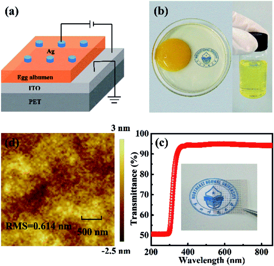
In the first stage of our experiments, we studied the switching performance and evaluated the mechanical flexibility of egg albumen based RRAM device. The commercial ITO/PET substrate was selected as the bottom electrode (BE) in the metal–insulator–metal (MIM) structure of our memory cell, as illustrated in Fig. 1(a). The albumen layer was spin-coated on the ITO/PET substrate with a speed of 6000 rpm for 30 s and subsequently dried in the ambient air. Finally, the Ag TEs were thermally evaporated on the albumen film through a shadow mask with a diameter of 500 μm. Fig. 1(b) shows the photographs of a chicken egg and the extracted egg albumen. Fig. 1(c) displays the transmission spectra of egg albumen and the fabricated Ag/egg albumen/ITO/PET device. The pure film of egg albumen has a high transmittance (∼95%) in the visible region, indicating its notable transparent property and potential application for transparent display. As shown in Fig. 1(d), the root mean square roughness of albumen film is 0.614 nm, which is examined by AFM (Dimension Icon from Bruker) and suggests a high uniformity of the albumen film.
 |
| | Fig. 1 (a) Schematic of the Ag/egg albumen/ITO/PET memory device. (b) Photographs of a chicken egg and the extracted egg albumen. (c) The transmission spectra of egg albumen and the fabricated Ag/egg albumen/ITO/PET device. (d) AFM image of albumen film with the root mean square roughness of 0.614 nm. | |
In the second stage of our experiments, we demonstrated the transferable and conformal egg albumen based RRAM device. In that case, the structure of Ag/egg albumen/Al/PVP/SiO2/Si was employed in device fabrication, in which the Al supporting layer with good ductility was selected as BE. Fig. 2 illustrates the schematic fabrication processes of the transferable device. Firstly, the PVP sacrificial layer and Al BE were spin-coated and thermal evaporated on the SiO2/Si substrate in sequence (Fig. 2(a) and (b)). Then, the albumen film and Ag TEs were prepared above Al layer using the same experimental conditions as the first stage (Fig. 2(c) and (d)). Subsequently, after immersing the device into water for 30 minutes, the memory cell of Ag/egg albumen/Al can be delaminated from SiO2/Si substrate and became free-standing through dissolving the PVP layer (Fig. 2(e)). Eventually, the delaminated device can be transferred onto arbitrary substrates (Fig. 2(f)). The electrical characterizations of egg albumen based RRAM were carried out by using a Keithley 2636A semiconductor analyzer, an arbitrary function generator (3390, Keithley) and an oscilloscope (TDS 2012B, Tektronix).
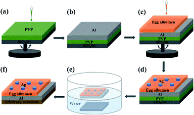 |
| | Fig. 2 Schematic diagram of the fabrication processes for the transferable Ag/egg albumen/Al RRAM device by using a water-dissolution method. (a) PVP, (b) Al BE, (c) egg albumen and (d) Ag TEs were grown on the SiO2/Si substrate in sequence by using spin-coating and thermal evaporation methods. (e) Delamination of Ag/egg albumen/Al device from original substrate through dissolving the PVP layer in water, and (f) the obtained transferable device. | |
Results and discussion
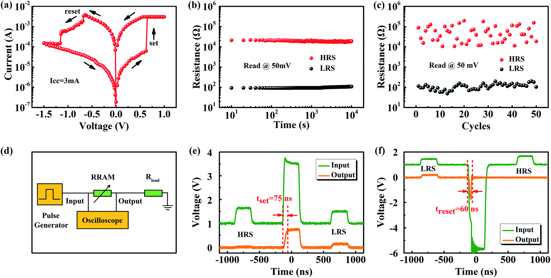
Fig. 3(a) shows the typical I–V curves of Ag/egg albumen/ITO/PET memory cell with a bipolar RS behavior. As applying positive bias on Ag TE, the current abruptly increased to the compliance current (3 mA) at around 0.6 V (defined as set voltage, Vset), leading to the device switching from high resistance state (HRS) to low resistance state (LRS). Conversely, when the applied negative bias reached a reset voltage (Vreset) of ∼−0.7 V, the current dropped and the resistance state changed from LRS to HRS. As shown in Fig. 3(b), both the HRS and LRS can retain their resistances without apparent degradation up to 104 s, indicating their long-time retention. Fig. 3(c) shows the evolution of HRS and LRS in 50 consecutive RS cycles with a switching window of ∼100, confirming its reproducible characteristic of our memory device. Furthermore, high-speed switching also can be obtained in current memory cell. Fig. 3(d) shows the setup for RS-speed measurement, which consists of a pulse generator, an oscilloscope, a memory cell and a load resistor.33 Herein the load resistor of 500 Ω was connected in series to serve as one current limiter. The switching of resistance states were monitored by the read pulses [0.6 V/250 ns] before and after set pulse [2.5 V/250 ns] and reset pulse [−6 V/250 ns]. As shown in Fig. 3(e) and (f), the set and reset time were about 75 ns and 60 ns respectively, which ensured the egg albumen based RRAM a fast RS speed. All above results verified the acceptable RS performance of the egg albumen based RRAM device for storage application.
 |
| | Fig. 3 (a) Typical I–V curves and (b) the evolution of HRS and LRS with time. (c) The distribution of HRS and LRS in 50 consecutive RS cycles of Ag/egg albumen/ITO/PET memory device. (d) Schematic diagram of a setup for RS-speed measurement. (e and f) The obtained set and reset switching processes by monitoring input and output signals in the RS-speed test. | |
In order to probe the switching mechanism of egg albumen based RRAM device, the local conductivity distribution of the Ag/egg albumen/ITO cell was further investigated using C-AFM. Herein, the scanning area was 1 × 1 μm2 and the current distribution topography was measured at a read voltage of 10 mV after set and reset processes. The HRS had a very low conductance as shown in Fig. 4(a). In comparison, after setting the device to LRS, the highly conductive paths in local regions can be seen in Fig. 4(b). Thus, the C-AFM measurement provided a straightforward evidence to support the filamentary mechanism of our device. To investigate the conduction of HRS and LRS, the switching I–V curves were redrawn in log–log scale as shown in Fig. 4(c). Both the I–V curves of HRS and LRS can be well fitted by straight lines with the slope of 1, indicating their ohmic conduction, which is consistent with Chen's study.21 Previous reports usually attributed the switching mechanism of albumen based RRAM to formation of Fe filaments inside the albumen layer when using common electrodes (e.g., Al, W, Mg).21,25 However, it may be not applicable for our Ag/egg albumen/ITO device since the active Ag TE has a high possibility for cations migration during switching process. Considering the structure of our memory device, one primary speculation is that the formation and rupture of Ag conducting channel is responsible for RS mechanism.34,35 In fact, the evolution of Ag migration into albumen film was observed during set process via an optical microscope (see Fig. S1 in ESI†) and was recorded by a CCD camera (see ESI Movie S†). However, the Ag filaments with continuous structure need to be eliminated according to the results of temperature dependence of HRS and LRS. For HRS, there was no apparent temperature dependence in our RRAM cell (see Fig. S2 in ESI†), indicating an electrical characteristic of insulator. In comparison, the LRS decreased with increasing temperature as shown in Fig. 4(d), which exhibits the non-metallic feature and excludes the existence of continuous Ag filaments inside the albumen film. In addition, the inset of Fig. 4(d) shows a linear relationship between ln(R) and T−1/2, which is consistent with the equation of electron hopping process:
| | |
σ ≈ exp(−2(C0/kBT)1/2)
| (1) |
where
σ is the conductivity,
C0 is the average spacing between nanoclusters,
kB is the Boltzmann constant.
36–38 Thus, the above relationship verified the electron hooping conduction in LRS.
36–38 As reported by Yang
et al. and Gao
et al., the cations preferred to capture free electrons from the dielectric when the migration happens in the RS layer with low cation mobility, leading to the formation of metal nanoclusters instead of continuous metal filaments.
39,40 This kind of Ag nanoclusters has also been reported by Wang
et al. when studying the switching mechanism of sericin protein based RRAM with Ag TE.
41 Therefore, the switching mechanism can be understood as the formation and dissolution of discrete Ag nanoclusters rather than continuous Ag filaments.
Fig. 4(e) illustrates the schematic diagram of RS mechanism in current device. In the set process, the Ag ions were produced by an oxidation process when applying positive bias on Ag TE (
Fig. 4(e) – SET). Due to the low cation mobility in albumen, Ag ions by the side of TE were reduced through capturing the electrons form BE, resulting in the growth of Ag filaments comprising of nanoclusters.
39,40 Then, the electrons can flow through these nanoclusters with a hopping conduction, and memory device switched from HRS to LRS (
Fig. 4(e) – LRS). In reset process, as applying negative bias on the TE, the Ag nanoclusters were oxidized and migrated back due to the Coulomb repulsion produced by BE (
Fig. 4(e) – RESET), leading to the rupture of filaments near the BE (
Fig. 4(e) – HRS), the device switched from LRS to HRS.
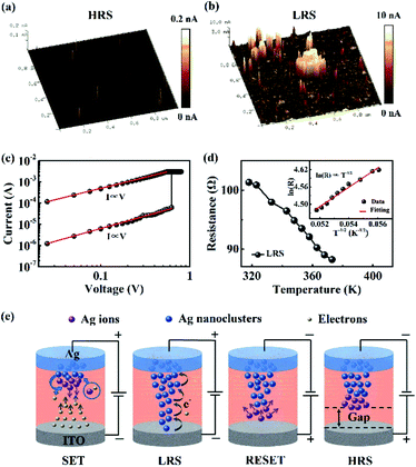 |
| | Fig. 4 The local conductivity distribution of the Ag/egg albumen/ITO cell in HRS (a) and LRS (b) as measured by C-AFM. (c) Experimental and fitted I–V cures in log–log scale for Ag/egg albumen/ITO/PET structure. (d) The temperature dependence of LRS, inset: a linear relationship of ln(R) ∼ T−1/2. (e) Scheme of hopping conduction mechanism comprising SET, LRS, RESET and HRS. | |
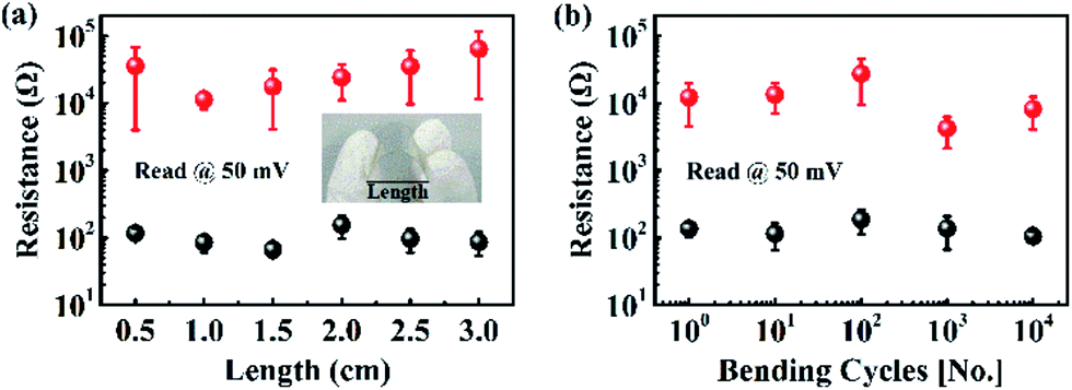
We studied the mechanical bending stability and bending endurance of Ag/egg albumen/ITO memory cell using PET as substrate (see Fig. 5). We fabricated device with the area of 3 × 3 cm2 and performed the mechanical tests with large bending angles and multiple bending cycles. The resistances were read under 50 mV at room temperature. As shown in Fig. 5(a), the 3 cm-long flat device was bent to different lengths of 2.5, 2.0, 1.5, 1.0, and 0.5 cm. Note that the average value of HRS/LRS had no obvious degradation with different bending angles except acceptable fluctuation. Furthermore, the evolution of device with bending cycles was also measured by using a mechanical vibrator with the frequency of 10 rps, as shown in Fig. 5(b). There was no apparent difference occurred for HRS and LRS when bending the device up to 104 cycles. All above tests suggested that the Ag/egg albumen/ITO/PET flexible memory device had excellent flexibility against mechanical stress and strain.
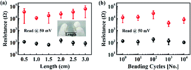 |
| | Fig. 5 Mechanical bending tests of Ag/egg albumen/ITO/PET flexible memory device. (a) The variation of HRS and LRS under different bending angles, inset: the measurement of length. (b) The bending cycles dependence of HRS and LRS. | |
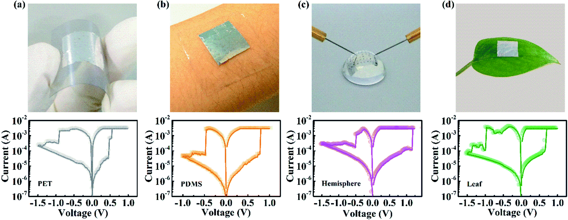
Another advantage of albumen based RRAM is its potential diversified features besides mechanical flexibility, such as skin-attachment, conformality, and biodegradability. In order to further study its possible applications, the Ag/egg albumen/Al devices were configured and transferred onto several nonconventional substrates using a water-dissolution method, as illustrated in the Experimental section (Fig. 2). Herein, the PET, polydimethylsiloxane (PDMS), glass dome hemisphere with 3-D surface and a leaf substrate were selected to demonstrate the feasibility of the transferable memory devices. Fig. 6(a)–(d) present the photographs and corresponding I–V curves of the Ag/egg albumen/Al RRAM devices, which were transferred onto the above-mentioned substrates. As shown in Fig. 6(a), the device was transferred onto PET substrate and showed good flexible property as the Ag/egg albumen/ITO/PET structure RRAM thanks to the van der Waals interaction between Al and PET. Fig. 6(b) exhibits the skin-attachable performance through transferring the device onto a biocompatible PDMS film, indicating its potential application for conformal electronics on biological surfaces. Furthermore, we transferred the RRAM device onto a glass dome hemisphere with 3-D curved surface to test the feasibility of device with non-planar platform. As shown in Fig. 6(c), there was no apparent bubbles or wrinkles on the whole surface of the glass dome hemisphere, confirming the close contact of memory device with 3-D objects. Finally, Fig. 6(d) shows the device that was transferred onto a leaf substrate with rough surface, which displays its compatibility with biodegradable substrate. Reliable RS characteristics can be found in these devices with Al BE (Fig. 6(a)–(d)), indicating their reproducible RS performance. The statistic HRS/LRS states were also collected from the devices with different substrates (see Fig. S3 in ESI†), which further verified the reliability of our device on diverse substrates. These above results suggested no mechanical damages occurred in the transfer process. This transferable albumen based RRAM is expected to achieve multiple functions by integrating device with diverse substrates.
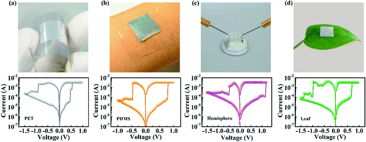 |
| | Fig. 6 Photographs of transferable devices onto various substrates and corresponding I–V curves. The nonconventional substrates include (a) flexible PET substrate, (b) biocompatible PDMS, (c) a glass dome hemisphere with 3-D surface and (d) a biodegradable leaf with rough surface. | |
Conclusion
In summary, the Ag/egg albumen/ITO based RRAM device was fabricated and presented reliable switching performance, including long retention time and fast switching speed. Its switching mechanism can be attributed to the formation and rupture of filaments composed of discrete Ag nanoclusters. The albumen based RRAM device showed excellent mechanical flexibility in the bending tests. Furthermore, the transferable Ag/egg albumen/Al device was demonstrated. By using a simple water-dissolution method, this device can be transferred onto desired substrates besides PET for future flexible applications with the diversified features. For instance, several nonconventional substrates were selected in this work, such as a glass dome hemisphere for a 3-D surface and a leaf for biodegradable applications. In particular, the device with PDMS substrate can display interesting applications such as conformal skin-attachment, portable healthcare and intra-body area network devices, which are worth detaily studying in next work. Our study expands the transferable and flexible RRAM device based on egg albumen and provides a feasible approach to combine flexibility with other diverse functions for flexible electronics in the future.
Acknowledgements
This work is supported by the NSFC for Excellent Young Scholars (No. 51422201), the NSFC Program (No. 51372035, 61505026, 61574031, 61404026 and 61604037), the “111” Project (No. B13013), the Fund from Jilin Province (No. 20160101324JC and 20160520115JH), the Fundamental Research Funds for the Central Universities (No. 2412016KJ003), Open Project of Key Laboratory for UV-Emitting Materials and Technology of Ministry of Education (130028611).
Notes and references
- M. Stoppa and A. Chiolerio, Sensors, 2014, 14, 11957–11992 CrossRef CAS PubMed.
- M. C. Choi, Y. Kim and C. S. Ha, Prog. Polym. Sci., 2008, 33, 581–630 CrossRef CAS.
- C. Wang, D. Hwang, Z. Yu, K. Takei, J. Park, T. Chen, B. Ma and A. Javey, Nat. Mater., 2013, 12, 899–904 CrossRef CAS PubMed.
- R. H. Kim, H. Tao, T. I. Kim, Y. Zhang, S. Kim, B. Panilaitis, M. Yang, D. H. Kim, Y. H. Jung and B. H. Kim, Small, 2012, 8, 2812–2818 CrossRef CAS PubMed.
- K. Nomura, H. Ohta, A. Takagi, T. Kamiya, M. Hirano and H. Hosono, Nature, 2004, 432, 488 CrossRef CAS PubMed.
- H. Gleskova, I. C. Cheng, S. Wagner, J. C. Sturm and Z. Suo, Sol. Energy, 2006, 80, 687–693 CrossRef CAS.
- T. Someya, T. Sekitani, S. Iba, Y. Kato, H. Kawaguchi and T. Sakurai, Proc. Natl. Acad. Sci. U. S. A., 2004, 101, 9966–9970 CrossRef CAS PubMed.
- A. L. Briseno, S. C. Mannsfeld, M. M. Ling, S. Liu, R. J. Tseng, C. Reese, M. E. Roberts, Y. Yang, F. Wudl and Z. Bao, Nature, 2006, 444, 913–917 CrossRef CAS PubMed.
- M. F. El-Kady, S. Veronica, D. Sergey and R. B. Kaner, Science, 2012, 335, 1326 CrossRef CAS PubMed.
- W. Zhu, M. N. Yogeesh, S. Yang, S. H. Aldave, J. S. Kim, S. Sonde, L. Tao, N. Lu and D. Akinwande, Nano. Lett., 2015, 15, 1883–1890 CrossRef CAS PubMed.
- Y. Liu, Y. Xie, Y. Liu, T. Song, K. Q. Zhang, L. Liao and B. Sun, Semicond. Sci. Technol., 2015, 30, 104004 CrossRef.
- H. Zhu, Z. Fang, C. Preston, Y. Li and L. Hu, Energy Environ. Sci., 2013, 7, 269–287 Search PubMed.
- S. Moreno, M. Baniasadi, S. Mohammed, I. Mejia, Y. Chen, M. A. Quevedo-Lopez, N. Kumar, S. Dimitrijevich and M. Minary-Jolandan, Adv. Electron. Mater., 2015, 1, 1500154 CrossRef.
- S. W. Hwang, C. H. Lee, H. Cheng, J. W. Jeong, S. K. Kang, J. H. Kim, J. Shin, J. Yang, Z. Liu and G. A. Ameer, Nano. Lett., 2015, 15, 2801–2808 CrossRef CAS PubMed.
- D. H. Kim, J. Viventi, J. J. Amsden, J. Xiao, L. Vigeland, Y. S. Kim, J. A. Blanco, B. Panilaitis, E. S. Frechette and D. Contreras, Nat. Mater., 2010, 9, 511–517 CrossRef CAS PubMed.
- R. Waser and M. Aono, Nat. Mater., 2007, 6, 833–840 CrossRef CAS PubMed.
- J. Zahurak, K. Miyata, M. Fischer, M. Balakrishnan, S. Chhajed, D. Wells, H. Li, A. Torsi, J. Lim and M. Korber, Presented in part at the Electron Devices
Meeting, San Francisco, CA, USA, December 2014, pp. 15–17, DOI:10.1109/IEDM.2014.7046994.
- A. C. Torrezan, J. P. Strachan, G. Medeiros-Ribeiro and R. S. Williams, Nanotechnology, 2011, 22, 485203 CrossRef PubMed.
- B. J. Choi, A. C. Torrezan, J. P. Strachan, P. G. Kotula, A. J. Lohn, M. J. Marinella, Z. Li, R. S. Williams and J. J. Yang, Adv. Funct. Mater., 2016, 26, 5290–5296 CrossRef CAS.
- H. Wang, B. Zhu, H. Wang, X. Ma, Y. Hao and X. Chen, Small, 2016, 12, 3360–3365 CrossRef CAS PubMed.
- Y. C. Chen, H. C. Yu, C. Y. Huang, W. L. Chung, S. L. Wu and Y. K. Su, Sci. Rep., 2015, 5, 10022 CrossRef CAS PubMed.
- S. Qin, R. Dong, X. Yan and Q. Du, Org. Electron., 2015, 22, 147–153 CrossRef CAS.
- N. R. Hosseini and J. S. Lee, Adv. Funct. Mater., 2015, 25, 5586–5592 CrossRef CAS.
- N. Raeis-Hosseini and J. S. Lee, ACS Appl. Mater. Interfaces, 2016, 8, 7326–7332 CAS.
- X. He, J. Zhang, W. Wang, W. Xuan, X. Z. Wang, Q. Zhang, C. G. Smith and J. Luo, ACS Appl. Mater. Interfaces, 2016, 8, 10954–10960 CAS.
- H. L. Chi, R. K. Dong and X. Zheng, Nano. Lett., 2011, 11, 3435 CrossRef PubMed.
- K. Chung, H. Beak, Y. Tchoe, H. Oh, H. Yoo, M. Kim and G. C. Yi, APL Mater., 2014, 2, 092512 CrossRef.
- X. Li, W. Cai, J. An, S. Kim, J. Nah, D. Yang, R. Piner, A. Velamakanni, I. Jung and E. Tutuc, Science, 2009, 324, 1312 CrossRef CAS PubMed.
- L. Gao, G. X. Ni, Y. Liu, B. Liu, A. H. Castro Neto and K. P. Loh, Nature, 2014, 505, 190 CrossRef CAS PubMed.
- G. A. Salvatore, N. Münzenrieder, T. Kinkeldei, L. Petti, C. Zysset, I. Strebel, L. Büthe and G. Tröster, Nat. Commun., 2014, 5, 2982 Search PubMed.
- W. J. Kang, C. H. Ahn, M. G. Yun, S. W. Cho, K. K. Ye, E. K. Da, B. Kim, H. K. Cho and Y. Kim, RSC Adv., 2016, 6, 63418–63424 RSC.
- Y. Lin, H. Y. Xu, Z. Q. Wang, T. Cong, W. Z. Liu, H. L. Ma and Y. C. Liu, Appl. Phys. Lett., 2017, 110, 193503 CrossRef.
- Z. Q. Wang, H. Y. Xu, L. Zhang, X. H. Li, J. G. Ma, X. T. Zhang and Y. C. Liu, Nanoscale, 2013, 5, 4490–4494 RSC.
- S. Wu, T. Tsuruoka, K. Terabe, T. Hasegawa, J. P. Hill, K. Ariga and M. Aono, Adv. Funct. Mater., 2011, 21, 93–99 CrossRef CAS.
- S. K. Vishwanath and J. Kim, J. Mater. Chem. C, 2016, 4, 10967–10972 RSC.
- P. Sheng, B. Abeles and Y. Arie, Phys. Rev. Lett., 1973, 31, 44–47 CrossRef CAS.
- R. J. Kennedy, P. A. Stampe, E. Hu, P. Xiong, S. Von Molnar and Y. Xin, Appl. Phys. Lett., 2004, 84, 2832–2834 CrossRef CAS.
- Y. Zhang, H. Wu, Y. Bai, A. Chen, Z. Yu, J. Zhang and H. Qian, Appl. Phys. Lett., 2013, 102, 233502 CrossRef.
- Y. Yang, P. Gao, S. Gaba, T. Chang, X. Pan and W. Lu, Nat. Commun., 2012, 3, 732 CrossRef PubMed.
- S. Gao, C. Song, C. Chen, F. Zeng and F. Pan, Appl. Phys. Lett., 2013, 102, 833 Search PubMed.
- H. Wang, F. Meng, B. Zhu, W. R. Leow, Y. Liu and X. Chen, Adv. Mater., 2015, 27, 7670–7676 CrossRef CAS PubMed.
Footnote |
| † Electronic supplementary information (ESI) available. See DOI: 10.1039/c7ra05237e |
|
| This journal is © The Royal Society of Chemistry 2017 |

 Open Access Article
 This Open Access Article is licensed under a Creative Commons Attribution-Non Commercial 3.0 Unported Licence
 *a,
Y. Lina,
W. Z. Liua,
J. G. Maa and
Y. C. Liua
*a,
Y. Lina,
W. Z. Liua,
J. G. Maa and
Y. C. Liua