
 Open Access Article
 This Open Access Article is licensed under a
 Creative Commons Attribution 3.0 Unported Licence
Chromium nitride as a stable cathode current collector for all-solid-state thin film Li-ion batteries†
Alejandro N. Filippin‡
 *a,
Michael Rawlence‡a,
Aneliia Wäckerlina,
Thomas Feurera,
Tanja Zündab,
Kostiantyn Kravchykab,
Maksym V. Kovalenkoab,
Yaroslav E. Romanyuka,
Ayodhya N. Tiwaria and
Stephan Buecheler*a
*a,
Michael Rawlence‡a,
Aneliia Wäckerlina,
Thomas Feurera,
Tanja Zündab,
Kostiantyn Kravchykab,
Maksym V. Kovalenkoab,
Yaroslav E. Romanyuka,
Ayodhya N. Tiwaria and
Stephan Buecheler*a
aLaboratory for Thin Films and Photovoltaics, Empa – Swiss Federal Laboratories for Materials Science and Technology, Überlandstrasse 129, CH-8600 Dübendorf, Switzerland. E-mail: alejandro.filippin@empa.ch; Stephan.Buecheler@empa.ch
bLaboratory of Inorganic Chemistry, ETH Zürich, Vladimir Prelog Weg 1, CH-8093 Zürich, Switzerland
First published on 22nd May 2017
Abstract
The development of highly oxidation resistant current collectors which are inert against lithium at elevated temperatures (>600 °C) and high potentials (3–5 V vs. Li+/Li) is required for the realization of high voltage, thin film, all-solid-state Li-ion batteries. This is due to the method of building such batteries using layer by layer deposition, requiring the first layer to remain stable during all subsequent processing steps. A new cathode current collector based on Cr2N thin films and prepared by reactive pulsed DC sputtering at 300 °C is reported here. By varying the nitrogen partial pressure in the reactor several CrxN thin film alloys are prepared and their microstructural and electrical properties are characterized. We demonstrate that the alloy with an estimated composition of Cr2.1N exhibits a relatively low sheet resistance of 2.6 Ω sq−1 for a ∼500 nm film, high oxidation resistance and no reaction with lithium up to 600 °C. Furthermore, we observed electrochemical stability in the potential range 3–5 V vs. Li+/Li. Finally, as a proof of concept the electrochemical behavior of cells using Cr2.1N thin films as a current collector for the high voltage cathode LiMn1.5Ni0.5O4 is presented.
Introduction
The demand for Li-ion batteries has been accelerated in the last few years due to the mass availability of cheaper and more powerful electronic devices such as smartphones, laptops and other electronic gadgets. Moreover, the fast-growing market of Li-ion batteries is expected to expand even further owing to the introduction of fully electric vehicles, reaching a predicted market of more than 50 billion USD by 2018.1 This growth has been accompanied by a strong increase in research and development in the field, aiming for higher energy densities and faster charge rates. Conventional Li-ion technology relying on a liquid electrolyte seems to be reaching a technological limit, mostly owing to the electrochemical stability issues and geometric restrictions related to the electrolyte, but there is still plenty of room for improvement in the emerging field of lithium-based solid state batteries.2 Not only is this technology intrinsically safer than their liquid electrolyte counterpart, but it also has the potential to overcome long-standing problems and limitations related to conventional Li-ion technology.3–5 Solid-state batteries can potentially offer a longer lifetime, higher charge/discharge rates, higher output voltage and higher energy density by implementing a suitable combination of materials and 3D (micro)architectures.5 Furthermore, all-solid-state batteries can be miniaturized for implementation in micro-devices and even made flexible, thus expanding their functionality.5–8The focus of this paper is on the development of the current collector for the cathode in all-solid-state thin film batteries. Contrary to conventional Li-ion batteries using a liquid electrolyte, such batteries are fabricated through the sequential growth of several layers, as shown in Fig. 1, which often require high temperatures during or after deposition for proper crystallization. This method places stringent requirements on the cathode current collector which must remain unaffected; specifically it must have good electrical conductivity, high temperature stability, corrosion resistance, electrochemical stability and inertness against lithium. Research into such materials for thin film batteries is rather rare as evidenced by the lack of scientific publications, while cathode current collectors for bulk batteries are already well established due to less demanding processing conditions.9–11
 | ||
| Fig. 1 Schematic representation of an all-solid-state thin film cell comprising the following layers: substrate (1), cathode current collector (2), cathode (3), solid-state electrolyte (4), anode (5) and anode current collector (6). | ||
Some of the functional cathode, electrolyte and anode materials require temperatures above 600 °C for proper crystallization.12–14 Therefore aluminum, which is the first choice as cathode current collector in conventional Li-ion cells, is not suitable because of its relatively low melting point of 660 °C and the formation of electrically insulating LiAlO2 at temperatures as low as 450 °C.15 Other alternatives like tungsten, nickel, chromium and several stainless steels have already been investigated but either react in the potential range of 4–4.5 V vs. Li+/Li or oxidize below 600 °C.11,16–18 Standard stainless steel (grade 304) contains both Cr and Fe which diffuse into the cathode material LiMn2O4 when annealed at 600 °C or above even for short annealing times of 1 hour, degrading the cathode performance.19 Noble metals such as gold and platinum also alloy with lithium and have a prohibitive cost for use in mass produced batteries.20,21
TiN has been proposed as current collector for Li-ion microbatteries22 although it shows poor stability in air at temperatures of 600 °C and above.23 Forming TiO2 that is vulnerable to reactions with lithium resulting in the formation of Li4Ti5O12.24
On the other hand, Cr2N has good mechanical properties and high thermal stability in vacuum up to 1120 °C.25–27 Furthermore, reactions with lithium is only observed at temperatures above 850 °C for long dwell times. The oxidation of Cr2N begins between 650–700 °C in air.28–30 Cr2N has so far not been investigated as a current collector despite its promising characteristics such as electrical conductivity which is around 10 times higher than CrN.
In this work thin films of CrxN alloys are fabricated by pulsed DC magnetron sputtering, a deposition technique that allows high deposition rates and is industrially scalable. The compatibility of Cr2N with the high voltage cathode LMNO is verified by high temperature post-annealing of LMNO thin films sputtered onto Cr2N, followed by assembly and testing of coin cells comprising of a LiPF6-based liquid electrolyte and lithium foil as anode. These results pave the way for future efforts on replacing the liquid electrolyte with a suitable solid-state alternative for constructing all-solid-state batteries.
Experimental section
CrxN thin films were deposited by pulsed DC magnetron sputtering of a chromium target (99.95% purity, Umicore) in a Balzers BAS 450 PM deposition system. The depositions were carried out at a pressure of 0.3 Pa on boron doped silicon (100) (Prime grade, University wafers), stainless steel coin spacers (16 mm diameter × 0.5 mm thickness, Grade 316L, Hohsen Corp.), soda lime glass (5 cm × 5 cm) and aluminum foil (25 μm thick, 99.45% – metals basis, Alfa Aesar) substrates, varying the Ar to N2 ratio for each composition. Prior to each deposition both the substrates and the Cr target were pre-sputtered for 5 minutes in pure Ar followed by the poisoning of the target with an Ar to N2 ratio of 3![[thin space (1/6-em)]](https://www.rsc.org/images/entities/char_2009.gif) :18 (sccm) for 5 minutes. The target power used in all cases was 0.32 W cm−2, the pulsing frequency was 100 kHz, the reverse time was 2 μs, the total pressure was fixed at 0.3 Pa, and the temperature of the substrates was fixed at 300 °C.
:18 (sccm) for 5 minutes. The target power used in all cases was 0.32 W cm−2, the pulsing frequency was 100 kHz, the reverse time was 2 μs, the total pressure was fixed at 0.3 Pa, and the temperature of the substrates was fixed at 300 °C.
The deposition time for Cr2N was tuned to obtain the desired thickness of approximately 500 nm with a rate of ∼900 Å min−1. Such a thickness was chosen to ensure a low resistivity of ∼1.1 × 10⁻⁴ Ω cm. 500 nm thin films of LixMn1.5Ni0.5O4 were deposited by RF magnetron sputtering as cathode material on Cr2N(500 nm)/stainless steel (SS) and Cr2N(500 nm)/Si for characterization, alternating layers of NiO (99.9% purity target, AJA International) and LiMn2O4 (99.9% purity target, Jiangyin Entret Coating Technology Co.) with additional layers of Li2O (99.9% purity target, TOSHIMA Manufacturing Co.) to compensate for the lithium loss. The deposition process was carried out at 220 °C at a pressure of 0.05 Pa (24Ar:1O2), the RF power of the LiMn2O4, NiO and Li2O targets was 1.23 W cm−2, 0.47 W cm−2 and 1.23 W cm−2, respectively, yielding a deposition rate of 8.5 Å min−1 (LiMn2O4), 0.75 Å min−1 (NiO) and ∼3 Å min−1 (Li2O). The deposition time of Li2O was set to 0.11 times that of LiMn2O4 and NiO. The annealing on Cr2N/SS or Cr2N/Si current collectors was performed at 600 °C during 3 hours and in some cases at 700 °C for 1 hour, using in all experiments a 10 °C min−1 heating ramp and allowing the samples to cool down naturally. The Mn to Ni ratio was measured by energy dispersive X-ray spectroscopy (EDX). The total quantity of cathode material in each cell was determined by weighing in an analytical balance (Mettler Toledo XS205 Dual Range, 0.01 mg readability) each substrate before and after deposition of LMNO, obtaining an average of approximately 0.5 mg of LMNO per coin cell measured.
SEM images were acquired in a FEG-SEM HITACHI S-4800 working at 5 kV to minimize electrical charging of the layers. EDX spectra were registered at 10 kV using a Bruker XFlash 6|10 X-ray detector with 121 eV resolution at Mn Kα and the standardless quantification was performed with the software ESPRIT from Bruker. X-ray diffractograms were obtained with a PANalytical X'Pert PRO diffractometer using the CuKα1 radiation in a Bragg–Brentano configuration, while the grazing incidence X-ray diffraction diagrams (GIXRD) were acquired in a PANalytical X'Pert PRO MPD diffractometer using CuKα1. Four-point probe resistivity measurements were done in a NAGY SD-600 sheet resistivity meter on the soda lime glass coated substrates with an error in the measured sheet resistance below 2%. X-Ray Photoelectron Spectroscopy (XPS) measurements were performed with monochromatized Al K-α X-ray source (PHI Quantum 2000 equipment) at room temperature on both Cr2N/SS and Cr2N/Si samples. The surveys were acquired with 117.4 eV pass energy, and single scans with 29.35 eV pass energy. The latter provides high resolution scans with a full width half maximum of 1 eV. Depth profiles were carried out with an Ar+ ion sputter gun, at acceleration voltage of 2 kV. Atomic concentrations were evaluated using MultiPak software.
Electrochemical measurements were conducted in air tight coin-type cells, as in the scheme from Fig. S1 in the ESI,† assembled in an Ar-filled glove box (O2 < 0.1 ppm, H2O < 0.1 ppm). Elemental lithium was employed as both reference and counter electrode in Li-ion half cells. As electrolyte 1 M LiPF6 (battery grade, Novolyte) in dimethylcarbonate and ethylene carbonate (1:1 EC/DMC by weight, Novolyte) with 3 wt% 4-fluoro-1,3-dioxolan-2-one (FEC, battery grade, Solvionic) was used. Pre-dried glass microfiber (GF/D, Whatman, 80 °C for 12 hours under vacuum) served as separator. LMNO cells were cycled between 3–5 V vs. Li+/Li. All electrochemical measurements were carried out at room temperature on MPG2 multi-channel workstation (BioLogic). Specific capacities and currents were quantified with respect to the mass of the electrode loading.
To test the electrochemical stability of the current collectors the same setup was used. In this case the current collectors were not coated with any electrode material and the electrochemical measurements were performed on aluminum coated with ∼500 nm of Cr2N (Cr2N/Al) and bare aluminum for comparison.
Electrochemical impedance spectroscopy (EIS) was performed on annealed (3 hours at 600 °C in air) LMNO deposited on Cr2N(500 nm)/Si(100). 100 nm thick gold top contacts were deposited by thermal evaporation at a pressure of ∼10−4 Pa and a rate of 1.2 Å s−1 onto the annealed LMNO, and copper wires were bonded to them with silver paste (see scheme in Fig. S16a†). The measurements were done at open circuit voltage in a VMP3 multichannel workstation (Bio-Logic) in the frequency range 1 MHz to 10 mHz and applying a bias of 100 mV.
Results and discussion
The evolution of the CrxN film composition and resistivity, with respect to the nitrogen–argon ratios during deposition are presented in Fig. 2. The Cr content was derived from EDX and decreases with with higher N2 ratios, while the resistivity increases substantially. The film thickness also decreases with higher N2 ratios. Above a N2/Ar ratio of 1.49 only CrN is obtained and the deposition rate continues to decrease. The thickness variation with the N2/Ar ratio is shown in Fig. S2.† | ||
| Fig. 2 Approximate composition (x) and resistivity of CrxN films on soda lime glass as function of Ar/N2 ratio in the sputtering gas. | ||
The XRD diagrams in Fig. 3 represent the phase evolution of the CrxN films deposited on soda lime glass when x varies from 1 to 2.1, observing a clear phase transition from cubic CrN (JCPDS 11-0065) to hexagonal β-Cr2N (JCPDS 35-0803).31,32 For comparison the XRD of a thin film of Cr prepared using only Ar is also shown in Fig. 3 (JCPDS 019-0323).33 The observed changes in the peak intensities, position and width between x = 1 and x = 1.6 can be attributed to differences in nitrogen content in the Cr–N solid solution. At x = 1.7 there seems to be a coexistence of the cubic and hexagonal phases, while at x = 1.9 the shoulder at the right of the Cr2N(111) peak could be a reminiscence of the cubic phase. For x = 2.1 only the peaks assigned to Cr2N hexagonal phase can be observed. The as-obtained Cr2N is a polycrystalline film with a slight preferred orientation in the (110) direction with a Lotgering factor of F(110) = 0.17,34 and the observed peaks are shifted compared to the reference pattern which might be attributed to residual stress in the film (Fig. S3†). We observe that the phase evolution in Fig. 3 corresponds well to the x value obtained via EDX.
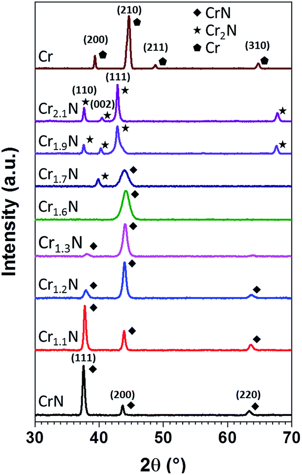 | ||
| Fig. 3 X-ray diffractograms of CrxN thin films exhibiting different estimated Cr/N ratios prepared at 300 °C by pulsed DC magnetron sputtering. | ||
The microstructure change of CrxN thin films grown by pulsed DC magnetron sputtering was studied by SEM, revealing a noticeable difference in the microstructure and surface roughness of the films with different Cr content (Fig. 4a–d). The film cross-sections present a columnar microstructure for the CrN and Cr2.1N cases as seen in Fig. 4d. In the intermediate composition between Cr1.2N and Cr1.7N the columnar features become less defined as the composition reaches a value close to Cr1.6N giving rise to more compact films (Fig. 4d, S4 and S5†). At x = 1.7 the columnar features begin to reappear (Fig. S4†) which may be caused by the phase transition to Cr2N (Fig. 3). This correlates well with the XRD diagrams from Fig. 3 where it can be observed that, for x = 1.6, only a broadened CrN(200) peak is present. The higher deposition rates resulting from a lower N2 content in the gas mixture are offset by the growing density of the film as it changes to Cr2N. This results in a higher growth rate at higher x values. SEM images for other intermediate compositions can be found in Fig. S4 and S5.†
 | ||
| Fig. 4 SEM images of CrxN thin films with 3 different N2 contents prepared at 300 °C by pulsed DC magnetron sputtering, showing the surface roughness of the as-prepared samples, normal views (a–c), and their columnar morphology, cross sections in (d). | ||
The sheet resistance of Cr2.1N thin films of 489 nm was determined to be as low as 2.6 Ω sq−1, which is close to the estimated bulk value (data points and fitting shown in Fig. S7†). Furthermore, as the thickness of these layers increased, they evolve towards a more columnar and porous microstructure, presenting fully developed curved columns at ∼300 nm, as a result of our deposition configuration (moving substrate), as observed in the SEM images in Fig. S6† (SEM normal views in Fig. S8†). For the sake of simplicity and to emphasize that the chromium rich composition obtained corresponds mainly to the Cr2N phase, Cr2.1N will henceforth be referred to as Cr2N.
Electrochemical characterization of Cr2N films was performed on Al foil substrates (Cr2N/Al) aiming to simplify cell assembly using coin cell configuration. Aluminum foil is a commonly used cathode current collector in lithium ion batteries which is highly resistant to oxidation and has good electronic conductivity. The morphology and resistivity of Cr2N/Al films was identical to those formed on silicon and glass. Electrochemical stability measurements of Cr2N/Al films were done by cyclic voltammetry (CV) at a slow scan rate of 0.1 mV s−1 to reveal any signs of oxidation of Cr2N. The measurements in Fig. 5a and b show that during the first cycle both Al and Cr2N/Al current collectors have very low current density (about 10–20 μA cm−2) in the whole 2–5 V voltage range even at very high potentials proving high resistance to oxidation in Cr2N/Al films. Small signs of oxidation observed in Fig. 5a and b above 4.5 V vs. Li+/Li for both Cr2N/Al and Al current collectors can be assigned to the decomposition of the LiPF6 electrolyte itself,35 whereas the anodic peaks at 3.7 V and 4.2 V during the first cycle are usually attributed to the passivation of Al (note that Cr2N/Al has only one side coated with Cr2N).11 Moreover, after only 3 cycles Cr2N/Al current collector shows almost complete passivation evidenced by a negligible current density in the CV, closely resembling the behavior of Al.11
 | ||
| Fig. 5 Electrochemical performance of Cr2N/Al ∼500 nm thick CC in comparison with aluminum foil. (a) CVs of bare Al foil between 2–5 V vs. Li+/Li. (b) CVs of Cr2N/Al CC between 2–5 V vs. Li+/Li. | ||
In order to address the high temperature oxidation and lithium resistance of the Cr2N current collector, GIXRD and XPS studies were performed on LMNO/Cr2N. The high potential cathode material LMNO was deposited by RF-magnetron sputtering at a substrate temperature of 220 °C. At this temperature and low pressure (0.05 Pa) it is expected that the LMNO thin film presents a growth according to zone T in Thornton's structure zone model, i.e. not well defined fibrous grains, which is in agreement with SEM observations in Fig. S10, top.†36 Moreover, there is a diffuse interface between LMNO and Cr2N of roughly 50 nm (Fig. S9a†). The observed nano grains on the surface (Fig. S9b†) correlate well to the wide full-width-half-maximum observed in the XRD of the as-prepared LMNO (Fig. S9c†). After annealing at 600 °C for 3 hours significant changes occur to the LMNO/Cr2N multilayer as evidenced in the SEM cross section in Fig. 6b and described below. Compared to the as-prepared sample (Fig. S9a, b and S10,† top), the LMNO/Cr2N interface of the annealed sample is considerably thicker and has a higher porosity, while the Cr2N columns are now fused.
 | ||
| Fig. 6 (a) GIXRD of annealed LMNO(500 nm)/Cr2N(500 nm)/SS at grazing angles (ω) 1° and 5°; the green dashed lines indicate the Cr2N peaks. (b) SEM cross section of LMNO(500 nm)/Cr2N(500 nm)/SS. (c) Atomic ratios calculated from XPS sputter-depth profiles for LMNO(500 nm)/Cr2N(500 nm)/SS, the dashed line represents the LMNO surface and the dashed rectangle depicts the interface region between LMNO cathode material and Cr2N current collector. The thermal treatment was in all cases 600 °C for 3 hours. | ||
In addition to microstructural changes in the thin films, a polycrystalline second layer of LMNO can be seen after annealing. On the original LMNO film surface a large number of crystals form which increase in size up to ∼500 nm as the temperature is increased to 700 °C (Fig. S10, bottom, and S11†). The preferential diffusion of different cations towards the surface of LMNO has already been reported by Shin D. W. et al. and was attributed to the a possible structural stabilization driven by the surface free energy (σ).37 σ can be lowered by the presence of particles of different chemical nature to the surface, leading to the growth of surface crystals by heterogeneous nucleation.38 This phenomenon could explain the formation of crystals at 600 °C (Fig. 6b and Fig. S10,† middle) which is caused by the diffusion of chromium towards the surface and subsequent nucleation (see Fig. 6c). At 700 °C (Fig. S10, bottom, and S11†) large crystals grew at the LMNO surface in expense of Cr (from Cr2N) and LMNO, that now evidence a higher porosity. The diffractogram in Fig. 6a for LMNO(500 nm)/Cr2N (500 nm)/SS annealed at 600 °C for 3 hours indicates that LMNO is crystalline. For a grazing angle of 1° all the main peaks related to the Fd![[3 with combining macron]](https://www.rsc.org/images/entities/char_0033_0304.gif) m cubic spinel structure are clearly present (JCPDS 80-2162) and in perfect agreement with previously reported studies on LMNO layers deposited by sputtering. However, we are unable to distinguish whether the observed diffraction peaks originate from the surface crystals, the LMNO film, or a combination of both due to the proximity of Cr-doped LMNO lattice parameters39,40 On the other hand, when the angle is increased to 5° the peaks coming from the Cr2N current collector and stainless steel substrate are observed unchanged by the annealing treatment. A thicker Cr2N layer (1200 nm) has been chosen for the XRD analysis for a more pronounced view of the evolution of the Cr2N peaks, but the cells for electrochemical measurements were fabricated using a thinner Cr2N layer (500 nm).
m cubic spinel structure are clearly present (JCPDS 80-2162) and in perfect agreement with previously reported studies on LMNO layers deposited by sputtering. However, we are unable to distinguish whether the observed diffraction peaks originate from the surface crystals, the LMNO film, or a combination of both due to the proximity of Cr-doped LMNO lattice parameters39,40 On the other hand, when the angle is increased to 5° the peaks coming from the Cr2N current collector and stainless steel substrate are observed unchanged by the annealing treatment. A thicker Cr2N layer (1200 nm) has been chosen for the XRD analysis for a more pronounced view of the evolution of the Cr2N peaks, but the cells for electrochemical measurements were fabricated using a thinner Cr2N layer (500 nm).
For temperatures of 600 °C and above the surface area is increased due to the aforementioned formation of crystals which might lead to an enhancement of the performance at high cycling rates. The XPS sputter-depth profiles (Fig. S13.†) for LMNO(500 nm)/Cr2N(500 nm)/SS annealed at 600 °C for 3 hours revealed Cr incorporation into LMNO and some oxidation of Cr2N evidenced by the shoulder at higher binding energies in the Cr peaks around the 40.5 minute mark and a still prominent oxygen signal (Fig. S13†). Note that the nitrogen signal appears at this mark, indicating a coexistence of chromium oxide and chromium nitride at the interface, while at the 35.5 minute mark there is no nitrogen detected while the oxygen peak at lower binding energies can be assigned to a chromium oxide species (not incorporated into the LMNO). The atomic ratio calculated obtained from the XPS sputter-depth profile (Fig. S13†) is displayed in Fig. 6c, where it can be seen that the concentration of Cr is higher at the LMNO surface (sputter time 0, dashed line) in line with our hypothesis regarding the formation of crystals at the LMNO surface and the previously reported surface segregation observed for Cr-doped LMNO.37 The Mn/Ni ratio lies around 2.6 at the bulk of the LMNO while the N/Cr ratio (at the 50.5 minute mark) gives an approximate composition of the alloy of C2.4N, in good agreement with EDX data (Table ST1†) and in line with the GIXRD diagram from Fig. 6a. The dashed rectangle in Fig. 6c has been included to give an idea of the LMNO–Cr2N interface region. In the case of the 1 hour thermal treatment at 700 °C the concentration of Cr in the LMNO film is even higher than that of Ni, indicating a heavier oxidation of the Cr2N current collector as evidenced in Fig. S14† by broadened Cr peaks throughout the entire analyzed depth and a more intense oxygen peak even after 95 minutes of sputtering, and a much higher Cr/Mn ratio (Fig. S15†). In addition, this higher concentration of Cr is correlated with the presence of larger crystals when compared to the 600 °C thermal treatment for 3 hours. However, Cr doping has been demonstrated to be an effective way to stabilize the LMNO cathode, so it can expected that the incorporation of a certain amount of this element into LMNO has no negative effect on its performance.37 XPS surveys can be found in Fig. S12.†
In order to assess the electrochemical characteristics of the LMNO/Cr2N multilayer, through-plane EIS was carried out. After annealing the multilayer for 3 hours in air at 600 °C, 100 nm thick gold top contacts were deposited via evaporation onto the LMNO and copper wires were bonded to them with silver paste as shown in the scheme of Fig. S16a.† The Nyquist plot shown in Fig. S16b† exhibits two arcs which were modeled with the equivalent circuit shown in the inset of Fig. S16b.† The first arc measured at ∼64 kHz had a resistance of 130 Ω cm2. Due to the high frequency here, it is likely that this response is caused by electronic transport. Therefore we assign this value to the charge transfer resistance at the interface between the current collector and cathode. Although this resistance value is higher than for pristine Cr2N, it is comparable to optimized interfaces in solid state battery systems which require high temperature processing.41 The second arc, with a resistance of 658 Ω cm2 and occurring at 919 Hz could correspond to movement of lithium ions in the LMNO. When factoring in the LMNO thickness of 500 nm a Li-ion conductivity of 7.6 × 10⁻⁸ S cm−1 is calculated. This corresponds well to other values found in literature.42
The CV curves of pure LMNO thin films (no binder or carbon black added) after annealing at 600 °C for 3 hours in Fig. 7a clearly present the double peaks associated to the oxidation/reduction of nickel in the voltage range 4.6–5 V vs. Li+/Li, while poor electrochemical activity was detected in the region 3.9–4.3 V consistent with the oxidation/reduction of manganese.43 The clear observation of the Ni redox peaks is another indication of a good electrical contact between the current collector and the cathode as shown by Caballero et al.43 Galvanostatic voltage profiles show very clear discharge–charge plateaus with reduced hysteresis after cycle 10 (Fig. 7b). The cycling behavior of LMNO annealed at 600 °C (Fig. 7c) depends strongly on the cycling rate, exhibiting the highest initial capacity but also fastest capacity fade for the lowest rate of 1C. At 5C the initial capacity is noticeably lower as expected due to the low ionic and electronic conductivity of LMNO,42 and the fast charge rate (equal to the discharge rate). The faster degradation at lower rates suggests that the longer time spent at higher voltages is a contributing factor. This degradation can be assigned to the partial oxidation of liquid electrolyte and to the reaction/dissolution of Ni or Mn ions into the liquid electrolyte since we previously established the stability of Cr2N in this potential range (Fig. 5b),44–46 and to the presence of truncated particles on the LMNO surface (Fig. S10,† middle and bottom), besides octahedral ones, which have been reported to cause a poor performance/cyclability of LMNO.12 In addition, the cycling for the film annealed at 700 °C for 1 hour performed better (Fig. 7c), showing the slowest capacity fade and the highest coulombic efficiency probably because of an enhanced stability of the spinel structure upon cycling due to a higher incorporation of Cr3+ into LMNO (Fig. S14 and S15†) and bigger particle size at the surface, which in turn reduce the surface area (Fig. S10,† bottom).47 Note that the formation of LMNO thin films is not fully optimized. In order to considerably increase the performance of these cells it is mandatory to substitute the liquid electrolyte, which is unstable at high voltages, with a solid-state-electrolyte as demonstrated by J. Li et al.48
 | ||
| Fig. 7 Electrochemical performance of LMNO on Cr2N current collectors. (a) CV of LMNO annealed at 600 °C for 3 hours and then measured between 3–5 V vs. Li+/Li. (b) Galvanostatic charge and discharge curves of LMNO annealed at 600 °C for 3 hours. (c) Cycling behavior of LMNO annealed at 600 °C for 3 hours and 700 °C for 1 hour measured at different C rates. | ||
Conclusion
A range of CrxN thin films were deposited by pulsed DC sputtering by varying the Ar/N2 during deposition. The Cr content increased with the reduction of N2 content, while the resistivity decreased, reaching a value of ∼1.1 × 10⁻⁴ Ω cm for the composition Cr2.1N. With this stoichiometry the Cr2N columnar structure formed with a preferential orientation in the (110) direction as observed by XRD. The electrochemical stability of this alloy in a LiPF6-based electrolyte was proven in the voltage range of 3–4.8 V vs. Li+/Li. Moreover, the crystallization of LMNO at high temperature on the Cr2N current collector and the subsequent cycling have demonstrated the suitability of this material as a stable current collector for lithium containing cathode materials up to 600 °C in air. The observation of Cr diffusion into the cathode varies depending on the annealing temperature. Therefore, Cr2N is a promising cathode current collector for use in all-solid-state thin film batteries.Acknowledgements
Partial financial support from the Competence Centre for Energy and Mobility and the Swiss Electric Research (CCEM project SLIB number 911) and from the Swiss Federal Commission for Technology and Innovation (CTI) through the CTI Swiss Competence Centers for Energy Research (SCCER, “Heat and Electricity Storage”) is kindly acknowledged. We are grateful to the Laboratory for Energy Conversion Materials and the Laboratory for Nanoscale Materials Science at Empa in Dübendorf, Switzerland, for giving access to XRD and XPS equipment.References
- A. Vlad, N. Singh, C. Galande and P. M. Ajayan, Adv. Energy Mater., 2015, 5, 1402115 CrossRef.
- M. Hu, X. Pang and Z. Zhou, J. Power Sources, 2013, 237, 229–242 CrossRef CAS.
- J. C. Bachman, S. Muy, A. Grimaud, H.-H. Chang, N. Pour, S. F. Lux, O. Paschos, F. Maglia, S. Lupart, P. Lamp, L. Giordano and Y. Shao-Horn, Chem. Rev., 2016, 116, 140–162 CrossRef CAS PubMed.
- J. Kalhoff, G. G. Eshetu, D. Bresser and S. Passerini, ChemSusChem, 2015, 8, 2154–2175 CrossRef CAS PubMed.
- J. F. M. Oudenhoven, L. Baggetto and P. H. L. Notten, Adv. Energy Mater., 2011, 1, 10–33 CrossRef CAS.
- K. Sun, T.-S. Wei, B. Y. Ahn, J. Y. Seo, S. J. Dillon and J. A. Lewis, Adv. Mater., 2013, 25, 4539–4543 CrossRef CAS PubMed.
- S.-H. Kim, K.-H. Choi, S.-J. Cho, S. Choi, S. Park and S.-Y. Lee, Nano Lett., 2015, 15, 5168–5177 CrossRef CAS PubMed.
- Y. Kato, S. Hori, T. Saito, K. Suzuki, M. Hirayama, A. Mitsui, M. Yonemura, H. Iba and R. Kanno, Nat. Energy, 2016, 16030 CrossRef CAS.
- D. Peramunage, D. M. Pasquariello and K. M. Abraham, J. Electrochem. Soc., 1995, 142, 1789–1798 CrossRef CAS.
- A. H. Whitehead and M. Schreiber, J. Electrochem. Soc., 2005, 152, A2105–A2113 CrossRef.
- S.-T. Myung, Y. Hitoshi and Y.-K. Sun, J. Mater. Chem., 2011, 21, 9891–9911 RSC.
- A. Manthiram, K. Chemelewski and E.-S. Lee, Energy Environ. Sci., 2014, 7, 1339–1350 CAS.
- S. Lobe, C. Dellen, M. Finsterbusch, H.-G. Gehrke, D. Sebold, C.-L. Tsai, S. Uhlenbruck and O. Guillon, J. Power Sources, 2016, 307, 684–689 CrossRef CAS.
- J. Deng, Z. Lu, C. Y. Chung, X. Han, Z. Wang and H. Zhou, Appl. Surf. Sci., 2014, 314, 936–941 CrossRef CAS.
- T. K. Li and D. H. L. Ng, Mater. Sci. Eng., A, 2007, 445–446, 652–656 CrossRef.
- M. J. Graham and M. Cohen, J. Electrochem. Soc., 1972, 119, 879–882 CrossRef CAS.
- A. Warren, A. Nylund and I. Olefjord, Int. J. Refract. Met. Hard Mater., 1996, 14, 345–353 CrossRef CAS.
- S. Hallström, M. Halvarsson, L. Höglund, T. Jonsson and J. Ågren, Solid State Ionics, 2013, 240, 41–50 CrossRef.
- S. Komaba, N. Kumagai, M. Baba, F. Miura, N. Fujita, H. Groult, D. Devilliers and B. Kaplan, J. Appl. Electrochem., 2000, 30, 1179–1182 CrossRef CAS.
- A. D. Pelton, Bull. Alloy Phase Diagrams, 1986, 7, 228–231 CrossRef CAS.
- J. Sangster and A. D. Pelton, J. Phase Equilib., 1991, 12, 678–681 CrossRef CAS.
- J. Freixas, E. Eustache, P. Roussel, C. Brillard, D. Deresmes, N. Nuns, N. Rolland, T. Brousse and C. Lethien, J. Electrochem. Soc., 2015, 162, A493–A500 CrossRef CAS.
- H.-Y. Chen and F.-H. Lu, J. Vac. Sci. Technol., A, 2005, 23, 1006–1009 Search PubMed.
- G. Izquierdo and A. R. West, Mater. Res. Bull., 1980, 15, 1655–1660 CrossRef CAS.
- G. A. Zhang, P. X. Yan, P. Wang, Y. M. Chen and J. Y. Zhang, Mater. Sci. Eng., A, 2007, 460–461, 301–305 CrossRef.
- J. Lin, W. D. Sproul, J. J. Moore, S. Lee and S. Myers, Surf. Coat. Technol., 2011, 205, 3226–3234 CrossRef CAS.
- W. Ernst, J. Neidhardt, H. Willmann, B. Sartory, P. H. Mayrhofer and C. Mitterer, Thin Solid Films, 2008, 517, 568–574 CrossRef CAS.
- J. Cabana, C. D. Ling, J. Oró-Solé, D. Gautier, G. Tobías, S. Adams, E. Canadell and M. R. Palacín, Inorg. Chem., 2004, 43, 7050–7060 CrossRef CAS PubMed.
- C. Héau, R. Y. Fillit, F. Vaux and F. Pascaretti, Surf. Coat. Technol., 1999, 120–121, 200–205 CrossRef.
- Z. B. Qi, B. Liu, Z. T. Wu, F. P. Zhu, Z. C. Wang and C. H. Wu, Thin Solid Films, 2013, 544, 515–520 CrossRef CAS.
- E. T. Turkdogan and S. Ignatowiz, J. Iron Steel Inst., 1958, 188, 242 CAS.
- M. C. Morris, H. F. McCurdie, E. H. Evans, B. Paretzkin, H. S. Parker, W. Wong-Ng, D. M. Gladhill and C. R. Hubbard, Standard X-ray Diffraction Powder Patterns, U.S. Department of Commerce/National Bureau of Standards, Washington DC, 1985 Search PubMed.
- O. Brummer and W. Michel, Phys. Verh., 1961, 12, 19 Search PubMed.
- R. Furushima, S. Tanaka, Z. Kato and K. Uematsu, J. Ceram. Soc. Jpn., 2010, 118, 921–926 CrossRef CAS.
- A. Guéguen, D. Streich, M. He, M. Mendez, F. F. Chesneau, P. Novák and E. J. Berg, J. Electrochem. Soc., 2016, 163, A1095–A1100 CrossRef.
- J. A. Thornton, Proc. SPIE, 1988, 0821, 95–105 CrossRef CAS.
- D. W. Shin, C. A. Bridges, A. Huq, M. P. Paranthaman and A. Manthiram, Chem. Mater., 2012, 24, 3720–3731 CrossRef CAS.
- Zeolites and catalysis: synthesis, reactions and applications, ed. J. Čejka, A. Corma and S. Zones, Wiley-VCH, Weinheim, 2010 Search PubMed.
- L. Baggetto, R. R. Unocic, N. J. Dudney and G. M. Veith, J. Power Sources, 2012, 211, 108–118 CrossRef CAS.
- T. A. Arunkumar and A. Manthiram, Electrochim. Acta, 2005, 50, 5568–5572 CrossRef CAS.
- T. Kato, T. Hamanaka, K. Yamamoto, T. Hirayama, F. Sagane, M. Motoyama and Y. Iriyama, J. Power Sources, 2014, 260, 292–298 CrossRef CAS.
- M. Park, X. Zhang, M. Chung, G. B. Less and A. M. Sastry, J. Power Sources, 2010, 195, 7904–7929 CrossRef CAS.
- A. Caballero, L. Hernán, M. Melero, J. Morales, R. Moreno and B. Ferrari, J. Power Sources, 2006, 158, 583–590 CrossRef CAS.
- L. Yang, B. Ravdel and B. L. Lucht, Electrochem. Solid-State Lett., 2010, 13, A95 CrossRef CAS.
- Q. Wu, X. Zhang, S. Sun, N. Wan, D. Pan, Y. Bai, H. Zhu, Y.-S. Hu and S. Dai, Nanoscale, 2015, 7, 15609–15617 RSC.
- H.-M. Cho, M. V. Chen, A. C. MacRae and Y. S. Meng, ACS Appl. Mater. Interfaces, 2015, 7, 16231–16239 CAS.
- T.-F. Yi, Y. Xie, M.-F. Ye, L.-J. Jiang, R.-S. Zhu and Y.-R. Zhu, Ionics, 2011, 17, 383–389 CrossRef CAS.
- J. Li, C. Ma, M. Chi, C. Liang and N. J. Dudney, Adv. Energy Mater., 2015, 5, 1401408 CrossRef.
Footnotes |
| † Electronic supplementary information (ESI) available. See DOI: 10.1039/c7ra03580b |
| ‡ Indicates co-first author. |
| This journal is © The Royal Society of Chemistry 2017 |