 Open Access Article
Benzoquinoline-based fluoranthene derivatives as electron transport materials for solution-processed red phosphorescent organic light-emitting diodes†
So-Ra Parka,
Dong Heon Shina,
Sang-Mi Parkb and
Min Chul Suh *a
*a
aOrganic Electronic Materials Laboratory, Department of Information Display, Kyung Hee University, Dongdaemoon-Gu, Seoul 02447, Republic of Korea. E-mail: mcsuh@khu.ac.kr
bR&D Center OLED Team, AlphaChem, 145, Dongo 1-Gil, Hwaseong-Si, Gyeonggi-Do 18298, Republic of Korea
First published on 30th May 2017
Abstract
A new electron transport material (ETM) with two fluoranthene and a benzoquinoline moiety was synthesized for the fabrication of solution-processed phosphorescent organic light-emitting diodes (PHOLEDs). In particular, we designed a bulky structure with a large twisted angle and improved thermal stability as compared to those of the common ETMs [e.g., 2,2′,2′′-(1,3,5-phenylene)tris(1-phenyl-1H-benzimidazole) (TPBI)] for device stability. As a result, we found that 4-(3-(fluoranthen-3-yl)-5-(fluoranthen-4-yl)phenyl)-2-phenyl-benzo[h]quinoline (FRT-PBQ) showed high glass transition temperature (Tg: ∼184 °C) and moderately high electron transport behavior despite its bulky structural moieties. Moreover, we fabricated solution-processed red PHOLEDs with FRT-PBQ, and a relatively high current efficiency and external quantum efficiency of up to 20.7 cd A−1 and 15.5%, respectively, were achieved. In addition, the device lifetime was extended by a factor of 1.7 as compared to that of the device fabricated with TPBI as a common ETM.
Introduction
Active matrix organic light-emitting diodes (AMOLEDs) have received significant attention because of their advantages such as their ability to fabricate large-area displays and solid-state lighting. It is very difficult to manufacture large-area and high-resolution AMOLEDs as their production is based on the thermal vacuum deposition method, which results in a high manufacturing cost of mass production due to significant organic material consumption during deposition. Thus, to reduce the manufacturing cost, many research groups have focused on solution processes such as spin-coating, nozzle printing, and ink-jet printing.1–6 Due to these efforts, the efficiency of the devices has reached values similar to those achieved with vacuum deposition, but the lifetime of the devices is still considerably shorter.7 Thus, solution-processed OLEDs should be further developed to reach a level suitable for commercialization.The most important issue to obtain highly efficient solution-processed OLEDs is to realize multi-layer deposition without any mixing of each layer. In other words, it is important to have perfect orthogonality for each functional layer (e.g., hole transport layer (HTL) and emitting layer (EML)).7,8 To achieve orthogonal solubility, polymer-based cross-linkable materials have been used as HTLs for solution-processed OLEDs.1,2,9,10 However, cross-linkable HTLs mostly restrict the hole flow because of the lower hole mobility [μhole (cross-linkable HTL) ≈ 10−6 cm2 V−1 s−1] as compared to that of the commonly used HTL materials.1,2,11 As a result, the recombination zone of the solution-processed OLEDs should be shifted towards the HTL/EML interface although it could be the main reason for the deterioration of device lifetime as well as the induced exciton quenching.1,2 To solve this problem, we need to control the charge balance of the devices using various materials for EMLs and electron transport layers (ETLs).12–17 In this study, we focused on new electron transport materials (ETMs) for solution-processed OLEDs because the common ETMs normally exhibited very low glass transition temperature (TPBI = 124 °C), which resulted in a reduced device lifetime because of molecular crystallization from joule-heating of the devices.18 In other words, we report a new ETM with pretty high glass transition temperature (Tg) (about 184 °C) as well as moderately higher electron transport behavior than those of the reported previously ETMs [e.g. TPBI (2,2′,2′′-(1,3,5-phenylene)tris(1-phenyl-1H-benzimidazole)), BPhen (4,7-diphenyl-1,10-phenanthro-line) Alq3 (tris-(8-hydroxyquinoline) aluminum), etc.]. As a result, we obtained a moderately high device efficiency up to 20.7 cd A−1 using 4-(3-(fluoranthen-3-yl)-5-(fluoranthen-4-yl)phenyl)-2-phenyl-benzo[h]quinoline (FRT-PBQ).
Experimental
Instruments
1H NMR spectra were obtained using a Bruker AVANCE II 400 MHz NMR spectrometer. The absorption spectrum was obtained using a ultraviolet-visible (UV-vis) spectrophotometer (UV-1650PC). Photoluminescence (PL) spectra were acquired using a Perkin Elmer photoluminescence spectrophotometer (LS 55 model). Thermogravimetric analysis (TGA) was performed using TA INSTRUMENT TA4100. Differential scanning calorimetry (DSC) was performed using a Perkin Elmer model DSC-N650, operated under a nitrogen atmosphere. Matrix-assisted laser desorption/ionization time-of-flight mass spectrometry (MALDI-TOF MS) experiments were performed via a Bruker Daltonics model Ultraflex III MALDI TOF/TOF. High performance liquid chromatography (HPLC) was performed using a Waters model 2695 HPLC system. The positions of the highest occupied molecular orbital (HOMO) was measured using a photoelectron spectrometer (AC2, Riken Keiki). Carbon, hydrogen, and nitrogen analyses were conducted using an elemental analyzer (Flash1112/Flash2000, CE Instrument, Italy).Materials
The following materials were either purchased or synthesized. Poly(3,4-ethylene dioxythiophene) (PEDOT) doped with poly (styrenesulfonate) anions (PSS) (PEDOT:PSS) was purchased from Heraeus (Heraeus Clevios™ P VP CH 8000) as a hole injection layer (HIL) and HL-X026, a cross-linkable material (XM, T1: 2.25 eV), was purchased from Merck as an HTL.1,2,19,20 11-[2′-Diphenyl-[1,3,5]triazin-2-yl]-biphenyl-4-yl]-11H-benzo[a]carbazole as a red host material (RH, TRZ-PBC) was purchased from KISCO and iridium(III) bis(2-(3,5-dimethylphenyl)quinolinato-N,C2′)tetra-methylheptadionate, Ir(mphq)2tmd (Red Dopant, RD) was purchased from Lumtec and used as a phosphorescent red dopant for EML.1,2,21 In addition, FRT-PBQ was synthesized and used as a material for ETL. 2,2′,2′′-(1,3,5-Phenylene)tris(1-phenyl-1H-benzimidazole) (TPBI) as an ETL, lithium fluoride (LiF) as a material for an electron injection layer (EIL), and aluminum (Al) as a cathode were also purchased from commercial suppliers and used without purification.Materials synthesis of a new electron transport material
Device fabrication
To fabricate OLED devices with solution-processed red PHOLEDs, a 150 nm-thick patterned indium–tin oxide (ITO) glass with an open emission area of 4 mm2 was used. The ITO glass was cleaned in acetone and isopropyl alcohol via ultrasonication and rinsed in deionized water. Then, the ITO glasses were treated in UV-ozone to eliminate all the organic impurities that remained during the previous fabrication processes. PEDOT:PSS was spin-coated on an ITO glasses under ambient conditions and annealed at 150 °C for 15 min in a nitrogen atmosphere. Subsequently, the HTL material was dissolved in chlorobenzene at 0.5 wt% and spin-coated and cross-linked via the standard process. For the EML materials, the RH and red phosphorescent dopant (RD) were dissolved in toluene to obtain a 1 and 0.5 wt% solution. The red EML solution obtained by mixing the host and dopant solutions was spin-coated and dried at 100 °C for 10 min in a glove box. Then, the ETL was thermally deposited at a rate of 0.5 Å s−1 under typical vacuum conditions (<10−7 Torr). After the completion of all the solution and evaporation processes of the organic species, LiF and Al were successively deposited at 0.3 Å s−1 and 3 Å s−1, respectively.Measurements
The current density–voltage (J–V) and luminance–voltage (L–V) data of OLEDs were obtained using a Keithley SMU 2635A and Minolta CS-100A, respectively. The OLED area was 4 mm2 for all the samples studied in this work. Electroluminescence (EL) spectra and the Commission Internationale De'Eclairage (CIE) coordinates were obtained using a Minolta CS-2000A spectroradiometer.Results and discussion
Basic properties of FRT-PBQ
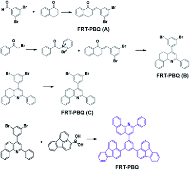
As previously reported, the carrier mobility μ of the hole and/or electron transport materials can be influenced by the molecular geometry of these materials (e.g. twisted angle between shell moieties, size of the pendant groups, planarity of the molecules near the core moiety, etc.). Especially, the mobility significantly decreases if the carrier hopping is limited due to the molecular geometry of these materials.22 In other words, μ is seriously affected by the molecular structure, which can cause molecular stacking through π–π interaction. Thus, μ increases if the hopping charge interacts with randomly oriented and located dipoles in the bulk film. However, Tg increases with molecular size and molecular weight. In other words, it normally increases if the sizes of the pendant moieties are bigger because they limit the segmental motion of the molecule. Based on these aspects, we synthesized a new ETM with two large fluoranthene and a benzoquinoline moiety for solution-processed OLEDs. Especially, we adopted the phenyl linker unit as a core moiety for these two fluoranthene and benzoquinoline moieties. As a result, we could increase the thermal stability as well as electron transporting behavior as compared to those of TPBI.23 The detailed synthetic route for the preparation of these materials is shown in Scheme 1.Fig. 1(a) and (b) show the molecular geometry of the ground state (S0) of TPBI and FRT-PBQ, which were obtained from the molecular simulation using the Gaussian 09 software. The HOMO and lowest unoccupied molecular orbital (LUMO) were optimized using Becke's three-parameter method and the Lee–Yang–Parr correlation (B3LYP) functional with the 6-31G (d) basis set. From this result, we found that the HOMO was mostly distributed over the entire molecule, whereas the LUMO was mostly localized on the fluoranthene and benzene core moieties, as shown in Fig. 1(b). This means that the electron transport process through the FRT-PBQ molecule may occur at the fluoranthene moiety although the benzoquinoline moiety has an electron-withdrawing heteroaromatic component. Moreover, the twisted angle of FRT-PBQ (between the fluoranthene moiety and the central phenyl linker) is about 53.8°. It was larger than that (about 34.0°) of TPBI (between the benzimidazole moiety and the central phenly linker), which may cause interruption of the π–π stacking. However, we could not expect that those twisted angles can interrupt to reduce the electron mobility because the planar fused aromatic systems such as fluoranthene and benzoquinoline moieties are large enough to be separated from the central core unit (e.g., phenyl linker). Moreover, these bulky and planar moieties could increase the thermal stability, as abovementioned. We also calculated the excited state of the FRT-PBQ molecule using the same theory (TD-DFT, B3LYP/6-311++G(d)) and obtained a triplet energy level (T1) of 2.30 eV, which is also summarized in Table 1.
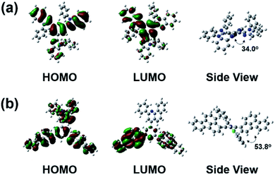 | ||
| Fig. 1 Optimized molecular geometry of (a) TPBI and (b) FRT-PBQ molecule showing HOMO (left), LUMO (middle), and side-view of the molecule (right). | ||
| Compound | λabsa [nm] | λplb [nm] | T1 [eV] (exp) | T1c [eV] (cal) | HOMO [eV] (AC2) | LUMO [eV] | Eg [eV] | Tg [°C] | Tm [°C] | Td [°C] | |
|---|---|---|---|---|---|---|---|---|---|---|---|
| 297 K | 77 K | ||||||||||
| a λabs: peak wavelength observed via UV-visible absorption spectroscopy (at 297 K).b λpl: peak wavelength measured from the photoluminescence (PL) spectra (at 297 K and 77 K).c T1 was calculated using the Gaussian 09W program [B3LYP, 6-311++G]. | |||||||||||
| FRT-PBQ | 246, 269, 290, 365 | 455 | 569 | 2.18 | 2.30 | −5.99 | −2.90 | 3.09 | 184 | — | 567 |
Fig. 2(a) displays the UV-vis absorption and PL spectra of FRT-PBQ. The band gap Eg that was determined from the band edge of the UV-vis spectrum was 3.09 eV for FRT-PBQ. The HOMO energy level measured by the AC2 analyzer and the LUMO energy level determined via the subtraction of the band gap from the HOMO energy level were −5.99 and −2.90 eV, respectively. Moreover, FRT-PBQ exhibited featureless emission spectral patterns, whereas some vibronic fine emission peaks were observed in the emission spectra obtained under low-temperature condition (77 K). From this spectrum, we confirmed the T1 of 2.18 eV for FRT-PBQ. In addition, we investigated the thermal stability behavior of FRT-PBQ, as shown in Fig. 2(b) and (c). As a result, the decomposition temperature Td and Tg were determined to be 567 and 184 °C for FRT-PBQ, respectively. As was expected, FRT-PBQ possesses much higher Tg of 184 °C as compared to those of common ETMs [e.g., Tg (TPBI) = 124 °C; Tg (TmPyPB) = 79 °C; and Tg (BPhen) = 66 °C], which might be due to its rigid structure.24 All the abovementioned data are also summarized in Table 1.
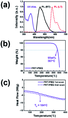 | ||
| Fig. 2 (a) UV-visible absorption and photoluminescence spectra, (b) TGA, and (c) DSC results of FRT-PBQ. | ||
Device engineering for highly efficiency OLEDs
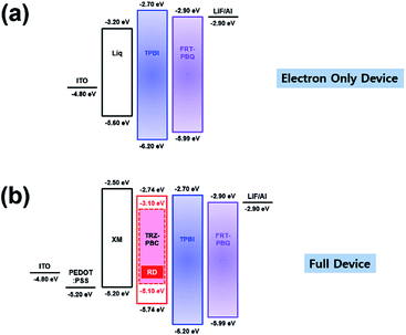
EOD A: ITO/LiQ (1.5 nm)/TPBI (100 nm)/LiF (1.0 nm)/Al (100 nm).
EOD B: ITO/LiQ (1.5 nm)/FRT-PBQ (100 nm)/LiF (1.0 nm)/Al (100 nm).
Fig. 3(a) shows the energy band diagram of the EODs of the ETMs. These materials exhibit LUMO energy levels of −2.70 and −2.90 eV for TPBI and FRT-PBQ, respectively. For this reason, we expected that FRT-PBQ might show better electron injection behavior than TPBI. However, we observed lower electron density from the EOD B (prepared with FRT-PBQ) as compared to that form the EOD A (with TPBI) at the voltage range less than 1.5 V. Hence, we cannot conclusively say that FRT-PBQ has better electron injection property than TPBI. In other words, the electron mobility of TPBI seems to be greater than that of FRT-PBQ at low electric field. Actually, we calculated the electron mobility of FRT-PBQ and TPBI from the space-charge-limited current (SCLC) region as follows in the next equation (eqn (1)):25
 | (1) |
 | (2) |
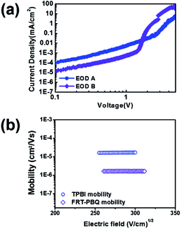 | ||
| Fig. 4 (a) J–V characteristics of the electron only devices with EOD A and EOD B and (b) calculated electron mobility for TPBI and FRT-PBQ from the SCLC region. | ||
As a result, the calculated electron mobilities are 1.70 × 10⁻⁵ and 1.66 × 10⁻⁶ cm2 V−1 s−1 for TPBI and FRT-PBQ, respectively, revealing the much lower electron mobility of FRT-PBQ than that of TPBI under low electric field. The electron mobility of FRT-PBQ is a reliable value because the TPBI mobility matches quite well with the previously reported value.26 From the results, it was observed that FRT-PBQ provided lower electron mobility than TPBI due to the increased twisted angle. However, the electron current density of FRT-PBQ rapidly increased in the higher voltage regions as aforementioned (>1.5 V) [see also Fig. 4(a)]. This type of reversal phenomenon in electron current density might be originated from the intrinsic molecular structure of FRT-PBQ. In other words, the weak electron accepting ability of FRT-PBQ presumably due to its lower polarity characteristic (1.5814 D) as compared to that of TPBI (2.4206 D) may cause relatively poorer electron injection behavior, whereas the flat and planar fluoranthene moieties help to efficiently transport the electron carriers at higher electric field region.27
Device A: ITO/PEDOT:PSS (40 nm)/XM (17 nm)/RH:RD (5%, 30 nm)/TPBI (50 nm)/LiF (1 nm)/Al (100 nm).
Device B: ITO/PEDOT:PSS (40 nm)/XM (17 nm)/RH:RD (5%, 30 nm)/FRT-PBQ (50 nm)/LiF (1 nm)/Al (100 nm).
The red PHOLEDs with TBPI and FRT-PBQ exhibited different device characteristics depending on the ETM, as shown in Fig. 5. Fig. 5(a) shows the current-density–voltage–luminance (J–V–L) characteristics. At a given constant voltage of 5.0 V (>1.5 V, as aforementioned), the current density values were found to be 0.16 and 1.57 mA cm−2 for device A and B, respectively. This is well consistent with the results obtained from the EODs. In other words, the higher current transporting behavior of FRT-PBQ makes device B much more electron conductive. For this reason, the turn-on voltages (Von) at a given constant luminance of 1 cd m−2 were 3.8 and 3.0 V for device A and B, respectively.
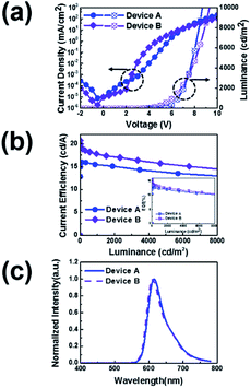 | ||
| Fig. 5 (a) J–V–L, (b) current-efficiency–L–power efficiency, and (c) normalized EL spectra of the fabricated red PHOLEDs (at brightness of 1000 cd m−2). | ||
In addition, the operation voltages (Vop) required to achieve 1000 cd m−2 were 6.7 and 6.0 V for device A and B, respectively (see Table 2). At a given constant luminance of 1000 cd m−2, the current and power efficiencies were 15.4 cd A−1 and 7.1 lm W−1 and 18.6 cd A−1 and 9.3 lm W−1 for device A and B, respectively, as shown in Fig. 5(b) and Table 2. In addition, this efficiency data correspond to the external quantum efficiencies (EQEs) of 11.1 and 13.0% for device A and B, respectively, as shown in the inset of Fig. 5(b). The maximum current and power efficiencies were 15.5 cd A−1 and 11.4 lm W−1 for device A and 20.7 cd A−1 and 21.7 lm W−1 for device B, respectively, as summarized in Table 2. In particular, the maximum EQE value of device A increased more than that of device B (i.e., device A: 11.4%; device B: 15.5%). From the abovementioned results, we found that the predominant electron transport characteristics were necessary because the devices fabricated with cross-linkable HTL materials via the solution process normally exhibited pretty low hole conductivity behavior. As a result, device B with higher electron transporting materials showed higher efficiency values although it displayed more serious roll-off behavior as compared to device A, plausibly due to its narrower recombination zone originating from its higher electron transporting property.
| Device | Vona/Vopb [V] | CE/PE/EQE [cd A−1/lm W−1/%] | CIE (x, y)bc | Lifetimeb (hours) | |
|---|---|---|---|---|---|
| Maximum | At 1000 cd m−2 | ||||
| a Measured at 1 cd m−2.b Measured at 1000 cd m−2.c CIE: Commission International de L'Eclairage. | |||||
| Device A | 3.8/6.7 | 15.5/11.4/11.4 | 15.4/7.1/11.1 | (0.65, 0.35) | 180.0 |
| Device B | 3.0/6.0 | 20.7/21.7/15.5 | 18.6/9.3/13.0 | (0.65, 0.35) | 301.4 |
Moreover, we investigated the EL spectral response, as shown in Fig. 5(c). From this measurement, we found that all the normalized EL spectra obtained from device A and B at a brightness of 1000 cd m−2 were almost the same, showing a maximum EL peak wavelength (λmax) of 611 nm.
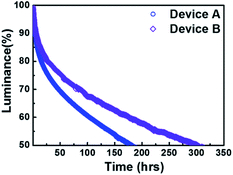
Finally, we measured the operational lifetimes of device A and B, as shown in Fig. 6. The lifetimes were measured under constant current density condition, giving rise to an initial brightness of 1000 cd m−2. The lifetimes at 50% drop of the initial brightness (T50) of device A and B were 180.0 and 301.4 h, respectively. Very interestingly, device B exhibited a much better lifetime behavior, which was 1.7 times higher than that of device A. This could be due to improved device efficiency as well as a reduction in the probability of crystallization and/or aggregation of the ETM during device operation, as abovementioned.
Based on these results, we believe that FRT-PBQ could provide fairly good device performances, including increased operational lifetime, because of its suitable electron transporting behavior as well as thermal stability when it is applied to solution-processed PHOLEDs.
Conclusions
In this study, we prepared a new ETM with a high glass transition temperature and superior electron transport behavior using two fluoranthene and one benzoquinoline-based moieties connected to a core phenyl linker unit. As a result, FRT-PBQ showed very good device performances when it was applied to solution-processed red PHOLEDs. Especially, the solution-processed red PHOLED devices fabricated in this study exhibited outstanding device efficiency as well as dramatically improved lifetime (by about 167.4%) as compared to those fabricated with common ETM such as TPBI.Acknowledgements
This research was supported by the Ministry of Trade, Industry & Energy (MOTIE, Korea) under the Industrial Technology Innovation Program. No. 10067715, ‘Development of crosslinkable organic materials for highly efficient multi-stacked OLEDs fabricated by continuous printing process’. This research was also supported by MOTIE (Ministry of Trade, Industry & Energy (project number #10051655)) and KDRC (Korea Display Research Consortium) support program for the development of future devices technology for display industry. Moreover, the authors are grateful to Mr Sang Kyu Kwak for his helpful assistance in verifying the purity of FRT-PBQ.Notes and references
- Y. R. Cho, H. S. Kim, Y.-J. Yu and M. C. Suh, Sci. Rep., 2015, 5, 15903 CrossRef CAS PubMed.
- M. C. Suh, S.-R. Park, Y. R. Cho, D. H. Shin, P.-G. Kang, D. A. Ahn, H. S. Kim and C.-B. Kim, ACS Appl. Mater. Interfaces, 2016, 8, 18256 CAS.
- K. S. Yook and J. Y. Lee, Adv. Mater., 2014, 26, 4218 CrossRef CAS PubMed.
- A. Hater, R. Anémian, R. Eberle, S. Heun, A. Ludemann, N. Schulte and H. Buchholz, J. Inf. Disp., 2011, 12, 57 CrossRef.
- N. J. Lee, D. H. Lee, D. W. Kim, J. H. Lee, S. H. Cho, W. S. Jeon, J. H. Kwon and M. C. Suh, Dyes Pigm., 2012, 95, 221 CrossRef CAS.
- H. C. Kim, S. I. Kwon, S. Y. Choi and K. C. Choi, J. Inf. Disp., 2015, 16, 179 CrossRef CAS.
- L. Duan, L. Hou, T. W. Lee, J. Qiao, D. Zhang, G. Dong, W. Liduo and Q. Young, J. Mater. Chem., 2010, 20, 6392 RSC.
- Y. J. Pu, T. Chiba, N. Aizawa, H. Sasabe and J. Kido, J. Photopolym. Sci. Technol., 2013, 26, 403 CrossRef CAS.
- H. S. Jeon, S. H. Cho, J. W. Seo, Y. S. Park and M. C. Suh, Thin Solid Films, 2013, 546, 176 CrossRef CAS.
- S. J. Cha, S. N. Cho, W. H. Lee, H. S. Chung, I. N. Kang and M. C. Suh, Macromol. Rapid Commun., 2014, 35, 807 CrossRef CAS PubMed.
- C. Xiang, N. Chopra, J. Wang, C. Brown, S. Ho, M. Mathai and S. Franky, Org. Electron., 2014, 15, 1702 CrossRef CAS.
- S. K. Kim, B. Yang, Y. I. Park, Y. Ma, J. Y. Lee, H. J. Kim and J. W. Park, Org. Electron., 2009, 10, 822 CrossRef CAS.
- C. W. Lee, K. S. Yook and J. Y. Lee, Org. Electron., 2013, 14, 1009–1014 CrossRef CAS.
- M. Kim and J. Y. Lee, Adv. Funct. Mater., 2014, 24, 4164 CrossRef CAS.
- S. J. Su, D. Tanaka, Y. J. Li, H. Sasabe, T. Takeda and J. Kido, Org. Lett., 2008, 10, 941 CrossRef CAS PubMed.
- S. J. Su, T. Chiba, T. Takeda and J. Kido, Adv. Mater., 2008, 20, 2125–2130 CrossRef CAS.
- X. Yang, G. Zhou and W. Y. Wong, Chem. Soc. Rev., 2015, 44, 8484 RSC.
- H. K. Kim, Y. H. Byun, R. R. Das, B. K. Choi and P. S. Ahn, Appl. Phys. Lett., 2007, 91, 093512 CrossRef.
- R. Po, C. Carbonera, A. Bernardi, F. Tinti and N. Camaioni, Sol. Energy Mater. Sol. Cells, 2012, 100, 97 CrossRef CAS.
- F. Huang, Y. J. Cheng, Y. Zhang, M. S. Liu and A. K. Y. Jen, J. Mater. Chem., 2008, 18, 4495 RSC.
- D. H. Kim, N. S. Cho, H. Y. Oh, J. H. Yang, W. S. Jeon, J. S. Park, M. C. Suh and J. H. Kwon, Adv. Mater., 2011, 23, 2721 CrossRef CAS PubMed.
- W. Y. Hung, G. M. Tu, S. W. Chen and Y. Chi, J. Mater. Chem., 2012, 22, 5410 RSC.
- S. Kumar and S. Patil, New J. Chem., 2015, 39, 6351 RSC.
- W. Y. Tan, R. Wang, M. Li, G. Liu, P. Chen, X. C. Li, S. M. Lu, H. L. Zhu, Q. M. Peng, X. H. Zhu, W. Chen, W. C. H. Choy, F. Li, J. Peng and Y. Cao, Adv. Funct. Mater., 2014, 24, 6540 CrossRef CAS.
- T. Y. Chu and O. K. Song, Appl. Phys. Lett., 2007, 90, 203512 CrossRef.
- W. Y. Hung, T. H. Ke, Y. T. Lin, C. C. Wu, T. H. Hung, T. C. Chao, K. T. Wong and C. I. Wu, Appl. Phys. Lett., 2006, 88, 064102 CrossRef.
- Y. Zhou, L. Ding, Y.-Z. Dai, N. Ai, J. Wang and J. Pei, Adv. Mater., 2012, 24, 957–961 CrossRef CAS PubMed.
Footnote |
| † Electronic supplementary information (ESI) available. See DOI: 10.1039/c7ra03178e |
| This journal is © The Royal Society of Chemistry 2017 |

