 Open Access Article
Creative Commons Attribution 3.0 Unported Licence
Ferroelectric fatigue in layered perovskites from self-energy corrected density functional theory
Kan-Hao Xueab,
Leonardo R. C. Fonsecac and
Xiang-Shui Miao *ab
*ab
aSchool of Optical and Electronic Information, Huazhong University of Science and Technology, Wuhan 430074, China. E-mail: miaoxs@hust.edu.cn
bWuhan National Laboratory for Optoelectronics, Wuhan 430074, China
cCenter for Semiconductor Components, University of Campinas, Campinas, São Paulo 13083-870, Brazil
First published on 19th April 2017
Abstract
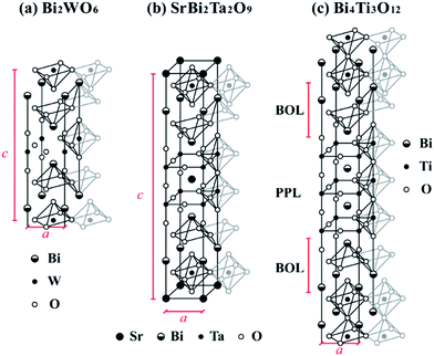
We employed self-energy corrected density functional theory (GGA-1/2) to investigate the band alignment between platinum and the layered perovskite Aurivillius ferroelectrics SrBi2Ta2O9 (SBT), Bi4Ti3O12 (BIT), and La-substituted BIT (BLT). The original GGA-1/2 method was found to not give satisfactory band gaps for these layered materials, despite yielding substantially better band gaps than GGA. We show that in such layered materials the cutoff radius for the self-energy potential in GGA-1/2 is strongly inhomogeneous across layers, therefore requiring different cutoff radii assigned to oxygen anions located in bismuth oxide layers and in pseudo-perovskite layers. After a 2D optimization of the oxygen cutoff radii, the calculated band gaps for these materials were found within 0.3 eV of experimental values. Next, we developed stoichiometric interface models for Pt/SBT and Pt/BIT, assuming platinum was connected to bismuth oxide layers as suggested by experiments. The calculated Schottky (hole) barriers for abrupt interfaces are 1.58 eV (2.50 eV) and 2.06 eV (1.41 eV) for SBT and BIT, respectively. For Pt(Bi) alloyed interfaces, where according to experiments some Bi diffuses inside the metal, we calculated a downshift of the Fermi level, lowering the barrier for holes. Because the barrier height for holes is lower in Pt/BIT than in Pt/SBT, a higher space-charge-limited-conduction hole current is expected to leak through metal alloyed Pt(Bi)/BIT/Pt(Bi) capacitors than to the corresponding SBT capacitors. Finally, replacing some Bi in the pseudo-perovskite layers with La significantly increased the barrier for holes. Based on the results above, we propose a phenomenological model for ferroelectric fatigue in Pt/BIT/Pt, whereby the formation of a non-ferroelectric Bi-deficient phase is the main reason for fatigue, which is accelerated by the lowered barrier for holes promoting the accumulation of Bi vacancies. The fatigue-free nature of Pt/SBT/Pt and Pt/BLT/Pt, on the other hand, stems from large barriers for both electrons and holes, which prevent the neutralization and further accumulation of charged defects. Our conclusions are consistent with the available experimental data.
1. Introduction
Ferroelectric random access memory1 (FeRAM), as a novel non-volatile semiconductor memory, has been successfully applied to smart IC cards and other embedded applications for decades. Two of its greatest challenges are ferroelectric fatigue2 and dielectric breakdown during polarization cycling,3,4 both of which jeopardize device reliability. Traditional FeRAM materials involve Pb- and Bi-containing perovskites5 and layered perovskites.6 Some Bi-containing Aurivillius-phase ferroelectrics such as SrBi2Ta2O9 (SBT) and Bi4−xLaxTi3O12 (BLT with x = 0.75, typically) are preferable since they are fatigue-free on top of conventional platinum electrodes.7,8 Initially the origin of such fatigue-free properties was attributed to SBT's [Bi2O2]2+ (BOL) layers, which are supposedly able to adjust their net space charge location in abeyance to the electro-neutral requirement.7 This explanation fails for Bi4Ti3O12 (BIT), another Aurivillius-phase ferroelectric with BOL layers, which reaches ferroelectric fatigue after ∼109 polarization cycles.3,9 Park et al. discovered that after substituting some La cations for the Bi cations within the pseudo-perovskite layers (PPLs) of BIT, the resulting BLT becomes fatigue-free on platinum electrodes.8 This is indeed a surprising discovery, explained with the argument that La substitution can stabilize the oxygen anions within the PPL. This explanation, however, was recently challenged by first-principles calculations,10 which revealed that La substitution only leads to a slight increase in the formation energy of neutral oxygen vacancies and cannot suppress the formation of the more probable +2 charged oxygen vacancies. Other explanations for the fatigue-free characteristic of BLT involve interface mechanisms11 and the formation of the anti-phase boundary.12 The exact reason why La substitution makes BIT fatigue-free is still far from settled.The recent discovery of ferroelectricity in HfO2 (ref. 13) has greatly enhanced the application potential of FeRAM and nonvolatile ferroelectric field effect transistors (FeFET) at the nanometer scale;14 nevertheless, ferroelectric Hf0.5Zr0.5O2 and other doped ferroelectric HfO2 compounds still suffer from ferroelectric fatigue4 as well as dielectric breakdown problems.15 Since the only family of “intrinsic” fatigue-free ferroelectrics are some of the Bi-based Aurivillius phase layered perovskites, a clear explanation for the origin of fatigue in these materials and how they become fatigue-free is still crucial for rationally addressing relevant problems in old and new ferroelectric materials. In particular, explaining the differences among SBT, BIT and BLT lies at the heart of this technology.
Based on the knowledge that La substitution cannot simply suppress the oxygen vacancy formation, in the present work we focus on the different interfacial properties between Pt and SBT, BIT and BLT, as the oxide interfaces are known to play a key role in the device performance.16,17 The measured Schottky barrier (SB) for Pt/SBT is between 0.8 and 1.29 eV,18–20 while for the Pt/BIT interface, we could not find an experimental value for SB in the literature. Liu et al. calculated the SB between Pt and BIT using empirical methods and found 1.2 eV,21 which is similar to SBT. Given that Pt/SBT and Pt/BIT possess similar SBs, it is then difficult to explain their great difference in leakage currents in terms of interface-limited mechanisms. Typical values for DC leakage current density in Pt/SBT/Pt and Pt/BIT/Pt capacitors are 10−7 A cm−2 and 10−5 A cm−2 under a 300 kV cm−1 bias, respectively.22,23 Moreover, the measured extraordinarily high leakage current through the Pt/BIT interface is far beyond the expected Schottky emission current based on a 1.2 eV barrier. Liu et al. thus ascribed the leakage current of Pt/BIT/Pt capacitors to bulk-limited leakage phenomena.21 Nevertheless, the authors failed to explain why carriers can overcome such a high barrier to lead to space-charge-limited-conduction (SCLC). In particular, the possible role of Pt alloy formation has rarely been discussed in previous theoretical works on BIT, though Pt alloys are well-known to serve as catalysts in fuel cells and other systems.24
To examine the possible role of ferroelectric/electrode interfaces on the leakage mechanism, ab initio calculations without empirical parameters are highly desired. In addition, to predict SBs numerically, it is necessary to perform accurate calculations of band gaps and band alignments for these complex Aurivillius-phase materials (typical examples are shown in Fig. 1) forming interfaces with metals, a task that often involves models comprising over 200 atoms. Standard density functional theory (DFT) calculation within the local density approximation (LDA) or generalized gradient approximation (GGA) normally yields substantially lower band gaps for semiconductors, limiting metal/semiconductor band offset calculations to the valence band offset only (hole barrier – HB), while the SB is inferred from the semiconductor experimental band gap.25 On the other hand, typical state-of-the-art methods such as the GW approximation26 and hybrid functionals27 can only handle supercells with a limited number of atoms. While hybrid functionals have been proven quite successful in studying defects in bulk solids,28,29 their numerical load is too high to model an interface between Pt and a complex Aurivillius-phase material. LDA+U30 is numerically efficient, but was originally designed for strongly correlated electron systems such as late 3d transition metal oxides. The application of LDA+U to Ti 3d orbitals in TiO2 does not yield an accurate band gap unless another Up parameter is also used in correspondence to O 2p orbitals.31 This suggests that LDA+U may be not suitable for column IV, V, or VI transition metals such as Ti, Ta, Nb, Mo and W, where strong electron correlation is not present. Hence, we shall first describe a new self-energy correction scheme (named GGA-1/2 (ref. 32)) within the ab initio framework that is computationally as efficient as LDA and GGA. Notwithstanding its many successes in accurately and efficiently predicting band gaps, we show that for layered materials, GGA-1/2 is improved, compared to GGA, but not enough in comparison to experimental data. Here, we identify the origin of the problem and propose a solution, and then utilize the improved scheme to investigate the band offsets between Pt and SBT, BIT and BLT.
This work is organized as follows: in Section 2, we describe GGA-1/2 and propose a new approach that is successful in the prediction of band gaps of several layered materials. In Section 3, we propose experiment-inspired interface models for the Pt/ferroelectric interfaces and correlate our calculated SBs obtained for several interface stoichiometries to experimental data. Based on the results of Section 3, in Section 4, we propose a general mechanism for fatigue in the materials considered.
2. Computational method
2.1 The GGA-1/2 method
For regular semiconductors without strong electron correlation effects, Ferreira et al. expanded the half occupation technique of Slater to modern DFT, and proposed the so-called LDA-1/2 and GGA-1/2 methods for solids.32,33 Unlike GGA+U, GGA-1/2 (here we only employ GGA-1/2, since LDA-1/2 yields similar results) is parameter-free and results in accurate band gap values for many elementary and binary semiconductors, such as Si and III–V compounds.34 Additionally, the computational load of GGA-1/2 is comparable to GGA. The method corrects the electron self-energy resulting from its interaction with the surrounding hole created by the repulsion of the electron cloud, a spurious consequence of the mean field approximation adopted in DFT. Despite extensive and successful tests in elementary and binary semiconductors and insulators, to our best knowledge, this method has never been tested for layered materials.In GGA-1/2, the self-energy correction for holes is applied to all anions in ionic semiconductors. In practice, the self-energy potential is obtained from the difference of atomic potentials between an isolated neutral atom and its ion with 1/2 electron stripped, which is then added to the pseudopotential of the corresponding atom (i.e., the anion) in periodic solid state calculations. The self-energy potential derived from atomic calculation is long-range in nature, but in solids it must be local in order to only correct the desired anion. Hence, a cutoff radius rcut is introduced in solid state calculations, which results in the trimmed self-energy potential Vs
 | (1) |
While the atomic pseudopotential is obtained for isolated atoms, making it transferable, the self-energy potential is strongly dependent on the materials. Indeed, the optimal rcut for a given species may vary from material to material. This must be the case since the hole localization in space depends on the charge distribution in the solid, in addition to the natural affinity for electrons of isolated atoms. This is not a drawback of the method, since the optimization of rcut is a straightforward calculation.
2.2 Failure of GGA-1/2 for layered materials
Before correcting the band gaps with GGA-1/2, the structural parameters of all materials considered in this work were obtained with regular DFT, as implemented in the plane-wave-based Vienna Ab Initio Simulation Package (VASP).35,36 We employed projector augmented-wave pseudopotentials37,38 and a plane-wave basis set with 500 eV cutoff energy. The electrons considered as the valence for some key elements are as follows: 5p, 5d and 6s for Pt; 4s, 4p and 5s for Sr; 6s and 6p for Bi; 3s, 3p, 3d and 4s for Ti; 4s, 4p, 4d and 5s for Nb; 5s, 5p, 5d and 6s for Ta; 5s, 5p, 5d and 6s for W; 5s, 5p, 5d and 6s for La; 2s and 2p for O. GGA was used for the exchange–correlation energy, within the Perdew–Burke–Ernzerhof39 (PBE) functional. All lattice parameters were fixed to experimental values (listed in the Appendix), while the atomic positions were relaxed until the residual forces were less than 0.02 eV Å−1. Once the structures were fully optimized, Vs was introduced in the relevant pseudopotentials and the calculation was repeated until self-consistency was achieved, without further relaxation of atomic positions.We applied the GGA-1/2 method to several titanates listed in Table 1 in order to verify the effectiveness of the self-energy correction, and then considered in more detail the special case of the Bi-containing titanate Bi4Ti3O12 (BIT). From CaTiO3 to BaTiO3, the GGA-1/2 band gaps are slightly larger, but quite close to experimental values (disagreement smaller than 0.3 eV), with the optimized cutoff radii at around 2.7 bohr, which is also the optimal cutoff value for rutile TiO2.
| Material | Phase | Band gap (eV) | O cutoff radius (bohr) | Experimental band gap (eV) | |
|---|---|---|---|---|---|
| GGA | GGA-1/2 | ||||
| TiO2 | P42/mnm | 1.86 | 3.14 | 2.7 | 3.0 (ref. 44) |
| CaTiO3 | Pbnm | 2.40 | 3.79 | 2.7 | 3.57 (ref. 45) |
| SrTiO3 | Pm3m | 1.90 | 3.40 | 2.7 | 3.25 (ref. 46) |
| BaTiO3 | P4mm | 1.85 | 3.29 | 2.9 | 3.27 (ref. 47) |
| Bi4Ti3O12 | B1a1 | 2.41 | 2.95 | 1.9 | 3.04 (ref. 41) |
| 3.08 (ref. 42) | |||||
| 3.64 (thin film)43 | |||||
| NaBiO3 | R![[3 with combining macron]](https://www.rsc.org/images/entities/char_0033_0304.gif) |
1.28 | 2.30 | 2.9 | 2.36 (ref. 48) |
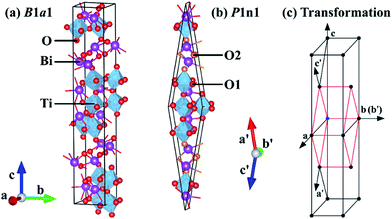
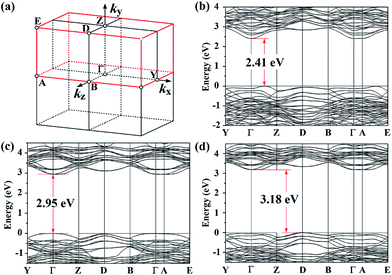
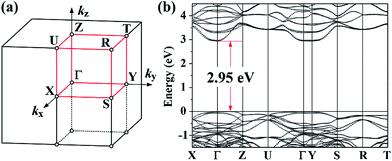
In the case of BIT, we considered its ferroelectric B1a1 phase, where the GGA-optimized structure is illustrated in Fig. 2(a). The non-standard B1a1 space group does not really correspond to a base-centered monoclinic structure. Rather, it can be reduced to a simpler monoclinic P1n1 primitive cell as indicated in Fig. 2(b) and (c). Since by chance the β angle of B1a1-BIT is 90°,40 the unit vector lengths along a′ and c′ axes are equal in the P1n1 primitive cell. Employing the latter, the calculated GGA-1/2 band gap for BIT is 2.95 eV, which is larger than the GGA band gap of 2.41 eV (Fig. 3(b)), but smaller than the values ranging between 3.04 eV and 3.64 eV (ref. 41–43) obtained experimentally. Note that the experimental values of 3.04 eV (ref. 41) and 3.08 eV (ref. 42) were obtained from bulk BIT, where the likely presence of defects created under their growth conditions and the finite temperature during data acquisition could yield a slightly reduced band gap. On the other hand, the 3.64 eV band gap43 was measured from BIT thin films, which tend to produce larger band gaps than bulk. Hence, a reasonable DFT band gap for BIT should lie between 3.04 eV and 3.64 eV. In addition, our GGA-1/2 calculation yields a direct Γ-to-Γ band gap (see Fig. 3(c)), whilst in the experiments BIT has an indirect band gap.41 Last but not least, the optimal cutoff radius for oxygen in BIT is only 1.9 bohr, considerably smaller than the previous three materials calculated (see Table 1).
The surprisingly small cutoff radius for oxygen offers some clues on why the band gap of BIT is underestimated by GGA-1/2. Using an overall oxygen cutoff radius of only 1.9 bohr, it is possible that the O self-energy potential has been trimmed artificially short, due to the different binding environments in the two layers, with O forming more ionic bonds in the PPL and more covalent bonds in the BOL. To answer this question, we used GGA-1/2 to calculate the band gap of NaBiO3, which involves Na+ dispersed in between BOLs. This example is relevant to our analysis since all of its anions are in the BOL. The GGA-1/2 calculation yielded a band gap of 2.30 eV for NaBiO3, close to the experimental value of 2.36 eV. More importantly, this was achieved using a relatively large cutoff radius for O of 2.9 bohr. Therefore, this result implies that our underestimation of the band gap in BIT stems from a much too low cutoff radius for O in the BOL.
To remedy this problem, we propose a local optimization scheme of the self-energy potential cutoff radii. Instead of using a uniform value for all O anions, we determine two cutoff radii, one for each group of O anions, here called O1 and O2 for O in the PPL and in the BOL (see Fig. 2(b)), respectively. This new method for GGA-1/2 is discussed in the next section.
2.3 Layered-dependent GGA-1/2
In light of the previous analysis, we re-calculated the band gap in BIT following the method below:1. Strip 1/2 electron from the 2p orbital of O1 atoms in the PPL to generate the self-energy potential. Determine the optimal cutoff radius variationally. Add the self-energy to the pseudopotential for O1 as in ref. 32.
2. Keep the O1 modified pseudopotential generated in step 1 fixed, then strip 1/2 electron from the 2p orbital of the O2 atoms in the BOL to generate another self-energy potential. Determine the cutoff radius variationally. Add the self-energy potential to the pseudopotential for O2 as in ref. 32.
We emphasize that the procedure above is to optimize the self-energy potential for each layer, while the atomic pseudopotentials remain the same. With the new method, we found that in BIT rcut is still 1.9 bohr for O1, but it increases to 3.1 bohr for O2. The resulting band gap for BIT increases to 3.18 eV, as shown in Fig. 3(d). Not only does this value fall within the range expected from the data, but the band gap is also indirect, in agreement with experiment. Our corrected BIT band gap is superior to the full electron calculation result by Singh et al.59 using the TB-mBJ functional, which yields an indirect 2.88 eV band gap. The quality of our BIT band gap is also comparable to the recent hybrid functional (HSE06) result obtained by Lardhi et al., who calculated a 3.6 eV indirect gap, while their measured gap was 3.3 eV.60
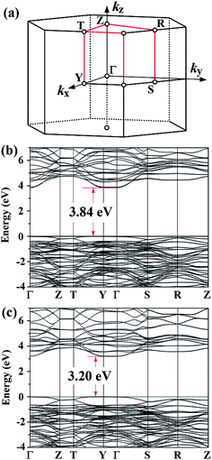
Following the same method, we calculated the electronic structures of two other Aurivillius-phase materials, SrBi2Ta2O9 and SrBi2Nb2O9, both with m = 2. Their structures are A21am,61,62 which can be reduced to a Cmc21 primitive cell. Despite being structurally isomorphic, their measured band gaps differ considerably. As shown in Table 2 and Fig. 4, the new method is successful in reproducing the data, while GGA and standard GGA-1/2 both fail. In the two materials the conduction band minima lie at the Γ point and the valence band maxima are close to the Y point. For SrBi2Ta2O9 the calculated indirect band gap is 3.84 eV, but the Γ-to-Γ direct band gap is very close, 3.87 eV; this implies that SrBi2Ta2O9 is almost a direct-band-gap insulator. In the case of SrBi2Nb2O9, the difference between calculated direct band gap (3.21 eV) and indirect band gap (3.20 eV) is even smaller. Notice that on using standard GGA-1/2, the band gaps of SrBi2Ta2O9 and SrBi2Nb2O9 are only 3.40 eV and 2.83 eV, respectively. It is therefore essential to use the layer-dependent anion cutoff radii for properly treating these two materials.
| Material | Phase | Method | Cutoff radii (bohr) | Calculated band gap (eV) | Experimental band gap (eV) | |
|---|---|---|---|---|---|---|
| SrBi2Ta2O9 | A21am | GGA | 2.60 | 4 (thin film)49 | ||
| GGA-1/2 | O 2p-1/2 | 2.3 | 3.40 | 4.1 (thin film)50 | ||
| O1 in PPL: 2p-1/2; O2 in BOL: 2p-1/2 | O1: 1.9; O2: 3.3 | 3.84 | 3.64 (powder)51 | |||
| SrBi2Nb2O9 | A21am | GGA | 2.32 | 3.4 (powder)52 | ||
| GGA-1/2 | O 2p-1/2 | 2.3 | 2.83 | 3.43 (ref. 53) | ||
| O1 in PPL: 2p-1/2; O2 in BOL: 2p-1/2 | O1: 1.9; O2: 3.3 | 3.20 | 3.44–3.54 (microcrystalline)54 | |||
| 2.72 (powder)55 | ||||||
| 3.60 (thin film)56 | ||||||
| Bi2WO6 | Pca21 | GGA | 2.07 | 2.69 (ref. 57) | ||
| GGA-1/2 | O 2p-1/2 | 2.2 | 2.36 | 2.7–2.85 (ref. 58) | ||
| O1 in PPL: 2p-1/2; O2 in BOL: 2p-1/2 | O1: 1.5; O2: 3.2 | 2.95 | ||||
For the m = 1 Aurivillius-phase ferroelectric Bi2WO6, we calculated its band structure using the new GGA-1/2 method with cutoff radii of 1.5 bohr and 3.2 bohr for O in the PPL and in the BOL, respectively. As shown in Fig. 5, the calculated band gap of 2.95 eV is almost in direct alignment with the bottom of the conduction band lying at Γ and the top of the valence band located along the Γ–Z direction. This band gap is larger than the reported experimental values.57,58 However, to the best of our knowledge, all reported band gaps for Bi2WO6 were measured from bulk samples grown at an intermediate temperature, since Bi2WO6 has been mainly employed as a photo-catalyst.63 Hence, it is possible that the true band gap of Bi2WO6 is larger than 2.85 eV, employing a higher synthesis temperature, which could lower the concentration of defects that may contribute to states near the band edges.
Among all the Aurivillius-phase compounds considered in this work, the optimal self-energy potential cutoff radii for O in the covalent BOL are in the range of 3.1 bohr to 3.3 bohr, exhibiting strong uniformity. The optimal cutoff radii for O in the ionic PPL, on the other hand, display much lower values, ranging between 1.5 bohr and 1.9 bohr.
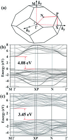
For the paraelectric I4/mmm phase of SBT and BIT, the new GGA-1/2 method yields 4.08 eV and 3.45 eV for the band gaps, respectively, slightly larger than their corresponding ferroelectric phases. As shown in Fig. 6, in the I4/mmm phase both materials show a CBM at the Γ point and a VBM at the X point. Since the I4/mmm phase is a high temperature phase in both materials, experimental investigations into their band structures are rather rare. For the sake of comparison, we also calculated their band gaps using other exchange–correlation functionals, shown in Table 3. While all GGA functionals predict relatively small band gaps, our GGA-1/2 results are quite close to the predictions of the hybrid functional HSE.
| XC/method | Band gap (eV) | |
|---|---|---|
| SBT | BIT | |
| PBE39 | 2.11 | 1.48 |
| PBEsol64 | 2.13 | 1.40 |
| revPBE65 | 2.16 | 1.53 |
| AM05 (ref. 66) | 2.07 | 1.44 |
| HSE06 (ref. 27 and 67) | 3.52 | 3.21 |
| GGA-1/2 | 4.08 | 3.45 |
2.4 Pt/SBT and Pt/BIT band alignment
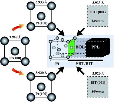
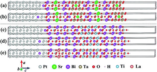
To reproduce as close as possible the available experimental data, under the size limitation constraint of our ab initio calculations, we constructed two interface models between Pt[100] and SBT[001], as well as between Pt[100] and BIT[001], where in both cases the dielectrics are in the I4/mmm phase. The lattice mismatch between the metal and the semiconductors are quite small for this phase (0.34% for Pt/SBT and −2.28% for Pt/BIT, respectively), similar to the solution adopted by Chon et al. to fit a Pt[100] substrate to epitaxially grown Nd-substituted BIT along the c-axis.68 The topology and construction scheme of our interfaces are illustrated in Fig. 7.Concerning interfaces between Pt and c-axis oriented SBT and BIT, there are two basic choices for interface configurations: Pt bonded to the PPL and Pt bonded to the BOL. Data from Auciello et al.69 suggest that Pt binds to the BOL of SBT. Furthermore, they also suggest that the Pt/SBT interface consists of an incomplete Bi-deficient BOL layer at the dielectric side and a BiPt alloy at the Pt side of the interface. Fig. 8(a) shows a model of Pt[100] bonded to a complete BOL layer, forming an abrupt interface. In this model the interfacial Bi atom connects to the hollow location of the Pt(100) surface, with a formation enthalpy of 0.38 J m−2 lower than the model with Bi lying on top of a Pt atom along the c-axis. Fig. 8(b) shows a diffuse interface model that captures the basic elements of the data from Auciello et al., where the top Bi atom has switched positions with one Pt atom resulting in an incomplete BOL layer bonded to a BiPt alloy. Because the size of our supercell is limited by our computational resources, the amount of Bi incorporation in the metal is likely to be exaggerated in our model. Nevertheless, the qualitative trends obtained are significant as discussed below.
In metal/dielectric interfaces, metal states penetrate the dielectric, forming the so-called metal induced gap states70 (MIGS), which strongly influence the electrical properties of the dielectric near the interface. In Fig. 9(a) and (b), we plot the layer-decomposed density of states (LDOS) for the two fundamental interface models (a) and (c) shown in Fig. 8. In both cases, the two bottom LDOS correspond to the platinum layers adjacent to the metallurgic junction. For the upper LDOS, the curves and the corresponding atomic layers shaded in red and blue stand for the BOL and the PPL, respectively. In both cases the MIGS only penetrate as far as the first BOL adjacent to the metallurgic junction, reflecting the fact that these dielectrics are highly effective in screening MIGS. In the central parts of the dielectrics, the conduction band edges mainly consist of the states from the PPL, though in the case of SBT the conduction band edge within the BOL is quite close to that of the PPL. For both interfaces, the location of the band edges does not vary deep inside the dielectric, rendering band offset extraction feasible.
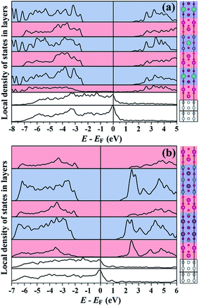 | ||
| Fig. 9 Local density of states for (a) abrupt Pt/SBT interface model as in Fig. 8(a); (b) abrupt Pt/BIT interface model as in Fig. 8(c). Each curve corresponds to a shaded region marked on the right side with the same background color. The white, red and blue backgrounds stand for Pt, BOL and PPL, respectively. | ||
In Fig. 10 and 11 we show the band alignments between the metal and the ferroelectric materials under investigation, obtained from the planar averaged potential (PAP).71 In this technique the averaged electronic potential along the atomic planes is used as a reference energy for the alignment of the bulk metal Fermi level and the semiconductor bulk band edges. As shown in Fig. 10(a) and (b), the SBs calculated with GGA and GGA-1/2 (based on the layered-optimized O cutoff radii) for the abrupt Pt/SBT interface (Fig. 8(a)), 1.34 eV and 1.58 eV respectively, do not differ very much. However, the HB calculated with GGA is merely 0.78 eV, while the value obtained with GGA-1/2 is 2.50 eV. GGA-1/2 corrects the band gap by partially removing the hole self-energy from occupied states in the valence band, thus more strongly lowering the valence band energy than raising the conduction band of the dielectric. For the diffuse interface (Fig. 8(b)), using GGA-1/2 (Fig. 10(c)) we found a much higher SB, 2.53 eV, and a much-reduced HB, 1.55 eV, compared to the abrupt interface model. Such strong modulation of the band alignment is caused by the increased transfer of charge from Pt to SBT in the model of Fig. 8(b) since O, now in direct contact with Pt, is more electronegative than Bi.
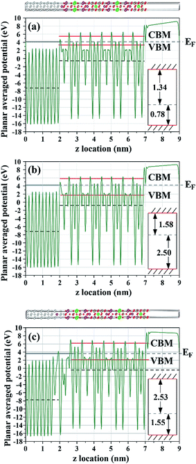 | ||
| Fig. 10 Electronic planar averaged potential (PAP) obtained for the Pt/SBT models with Pt bonded to the BOL. Horizontal dashed lines indicate the z-average of the PAP (see text for details) taken far from the surfaces and interface, while horizontal solid lines indicate the Fermi level and the band edges: (a) abrupt Pt/SBT interface model of Fig. 8(a) calculated with GGA; (b) abrupt Pt/SBT interface model of Fig. 8(a) calculated with GGA-1/2; (c) diffuse Pt(Bi)/SBT interface model of Fig. 8(b) calculated with GGA-1/2. Insets on the right indicate the location of the band edges (solid lines) with respect to the Fermi level (dashed line). The corresponding interface models of Fig. 8 are replicated on top of the PAP plots for clarity. | ||
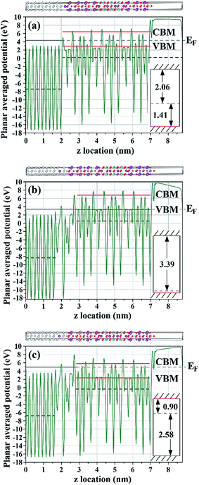 | ||
| Fig. 11 Electronic PAP profiles of Pt/BIT and Pt/BLT models, with Pt bonded to the BOL and calculated with GGA-1/2. Horizontal dashed and solid lines are as in Fig. 10: (a) abrupt Pt/BIT interface model of Fig. 8(c); (b) diffuse Pt(Bi)/BIT model of Fig. 8(d); (c) diffuse Pt(Bi)/BLT model of Fig. 8(e). Insets on the right indicate the location of the band edges (solid lines) with respect to the Fermi level (dashed line). The corresponding interface models of Fig. 8 are replicated on top of the PAP plots for clarity. | ||
Next, we consider the interface between Pt[100] and BIT[001], with Pt bonded to the BOL as in the previous models. An abrupt interface model is shown in Fig. 8(c), similar to the Pt/SBT model of Fig. 8(a). The interfacial Bi atom is connected to the hollow region of the Pt(100) surface, which is lower in formation enthalpy, about 0.37 J m−2 superior to the case of the Pt–Bi direct connection along the c-axis. The corresponding band alignment calculated with GGA-1/2 is shown in Fig. 11(a). In contrast to SBT, for BIT the HB is smaller than the SB, being 1.41 eV and 2.06 eV, respectively. In the case of a diffuse Pt(Bi)/BIT interface (Fig. 8(d)), the HB is reduced to merely 0.09 eV as shown in Fig. 11(b). The HB reduction between the abrupt and diffuse interfaces follows the same trend obtained for SBT, and in BIT it is small enough to establish an ohmic contact at the interface, allowing for SCLC current to flow through the dielectric.
Finally we consider the case of BLT, which has been shown to be very effective in minimizing the ferroelectric fatigue problem of Pt/BIT/Pt capacitors.8 Both experimental evidence72 and calculation results10 suggest that La tends to occupy the Bi site within the PPL. In Fig. 8(e) we propose a Pt(Bi)/BLT diffuse interface model with one La atom substituting one Bi atom within the PPL and Pt bonded to the BOL as in previous models. Fig. 11(c) shows that its HB sharply increases from 0.09 eV for Pt(Bi)/BIT to 2.58 eV for Pt(Bi)/BLT, while its SB decreases to 0.90 eV, smaller than the value obtained for Pt(Bi)/BIT, but still sufficient to avoid strong electron injection into the dielectric. The impact of La substitution in BIT on the Pt/BIT potential barrier is similar to Cu2+ substitution in CaTiO3.73
3. Model of ferroelectric fatigue and dielectric breakdown in BIT
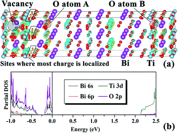
Ferroelectric fatigue is a complex phenomenon, which has inspired the proposal of several models such as domain wall pinning,74 dead interfacial layer,75 nucleation inhibition,76 dendrite growth,77 and local phase decomposition.78 For comprehensive reviews of existing models, the reader can refer to the works of Tagantsev et al.79 and Lou.2 Recently, Lou et al. proposed a universal model claiming that local phase decomposition caused by strong charge injection during polarization reversal and formation of a non-ferroelectric phase is the primary cause of fatigue in PZT.78 Unfortunately, he did not use this model to analyze the fatigue problem in BIT and the fatigue-free nature in SBT and BLT. Here, we extend Lou's model to BIT, BLT and SBT. Of the three, the only material showing fatigue in contact with Pt is BIT, while it is also the only material that forms ohmic contact with Pt in the case of some unintended BiPt alloy formation as revealed by our calculations presented in Section 2. The formation of a BiPt alloy layer near the interface is reasonable since during sample preparation an excess amount of Bi is usually used to compensate for its loss in thermal processes,80,81 as well as to suppress non-ferroelectric pyrochlore phases.9,82,83 In our work, we did not consider the scenario of isolated Bi vacancies in the ferroelectric or isolated Bi interstitials in Pt. However, if they are present, only neutral Bi vacancies or interstitials are expected, since the injection of holes can neutralize the likely −3 charged Bi defects if the Fermi level is lower than the defect state. Below, we prove that this is indeed the case for the Pt(Bi)/BIT interface, allowing for neutral Bi defects to accumulate during the voltage cycle (see discussion below) since there is no electrostatic repulsion between them. An accumulation of Bi vacancies in particular, may lead to a local phase decomposition when the amount of local Bi in the ferroelectric drops sharply. On the other hand, for the interfaces where the Fermi level alignment does not favor de-trapping of defect charge, the residual −3 charged Bi vacancies do not accumulate due to strong Coulomb repulsion. In summary, we expect the formation of a BiPt alloy near the Pt(Bi)/ferroelectric interface, where the Bi present in the alloy originates from excess Bi employed in the preparation process, which emerges from the swapping of Bi and Pt atoms near the interface, or from the formation of neutral Bi vacancies in the Bi-based dielectrics considered.It remains to be shown that charged Bi vacancies can be neutralized by electron transfer from the defect to the nearby metal in the Pt(Bi)/BIT case; to prove this point, we investigated the formation of one Bi vacancy in a 2 × 2 × 1 I4/mmm-BIT supercell. Since Bi vacancies prefer to stay in the PPL, as revealed by our previous study10 and by others,84 here, we focus on the PPL-located Bi vacancy and determine the degree of localization of the added 3 electrons. We therefore calculated the charge difference between a Bi3+ vacancy and a neutral Bi vacancy, keeping the relative locations of all atoms fixed for the charged and neutral systems. As shown in Fig. 12(a), these electrons are not trapped at the vacancy site, but mainly reside around the center of some Ti–O bonds surrounding the vacancy site, all within the same PPL. Some other regions such as A and B in Fig. 12 exhibit charge polarization induced by the defect. The polarization directions for both O atoms at sites A and B are such that the net electron cloud (yellow region) is pushed away from the vacancy site, confirming that the vicinity of the vacancy site is negatively charged. Next, to determine whether the charge localized in the region surrounding the Bi vacancy can be neutralized by the metal electrode, we calculated the energy levels associated with the Bi3+ vacancy. For this purpose, we relaxed the defective supercell with 3 extra electrons and calculated the partial density of states using GGA-1/2. As shown in Fig. 12(b), the energy band associated with the charged defects is ∼0.2 eV wide, and is separated from the VBM by ∼0.1 eV. The width of the defect band reflects the spread of the defect states in the atoms surrounding the Bi vacancy, while the location of the charged states near the VBM favors charge exchange with the metal in case the Fermi level is close to the VBM, and blocks charge exchange in case the Fermi level is higher in the band gap. The defect states alignment with the Fermi level occurs exactly in the case of Pt(Bi)/BIT, while in the other cases, namely Pt(Bi)/SBT, Pt(Bi)/BLT, Pt/SBT and Pt/BIT, they are below the metal Fermi level. Therefore, our interface models predict that only in the case of Pt(Bi)/BIT can electrons de-trap from the vicinity of the Bi vacancy. The resulting neutral Bi vacancies can accumulate during voltage cycles as explained below.
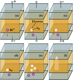
Fig. 13 provides a step-by-step illustration of our fatigue model in a Pt(Bi)/BIT/Pt(Bi) capacitor. Once device processing is completed, and even before any bias is applied to the capacitor, it is likely that some BiPt alloy is already formed at the interface, due to excess Bi used in sample preparation. In Fig. 13(a) the capacitor is under positive bias during the polarization cycling, during which some Bi3+ cations migrate to the cathode due to the electrostatic force. The remaining Bi vacancy and its vicinity can trap electrons to become negatively charged (Fig. 13(b)). The Bi vacancy state is low in the band gap and is separated from the bulk valence band maximum by a small energy (∼0.1 eV). When the electric field reverses (Fig. 13(c)), the trapped electrons can leak to the BiPt alloy depending on the relative position of the Fermi level with respect to the valence band of the dielectric. In the case of BIT in contact with a BiPt alloy electrode, the leak is possible since the electrode Fermi level is almost aligned with the top of valence band. The Bi vacancies become neutral and may continue to accumulate with the following electric field cycles (Fig. 13(e)). Local phase decomposition could then be triggered by the accumulation of Bi vacancies until the new non-ferroelectric Bi4−xTi3O12−y phase punches through the dielectric (Fig. 13(f)). This model is similar to the electroforming process in resistive random access memories (RRAMs);85,86 in RRAM, the new phase is conductive, made of fully-reduced metal clusters87 or conductive sub-oxides.88,89 However, during the polarization cycling of Pt/BIT/Pt capacitors, the new phase does not have to be conductive. If it is conductive, then the cell is broken-down, as reported in divalent metal substituted BIT thin films.90 Otherwise, the emergence of a new non-ferroelectric phase tends to reduce the overall polarization of the capacitor. The exact nature of this new phase is still unknown in BIT, but we infer that it is non-ferroelectric because it is Bi-deficient and Bi is well-known as the critical element for ferroelectric instability in BIT.10,91 In the limiting case, if all Bi atoms were removed, together with the associated oxygen atoms, then the resulting material would be TiO2, which is centro-symmetric and non-ferroelectric. In summary, our phenomenological model claims that missing Bi atoms is the main reason for ferroelectric polarization degradation of Pt/BIT/Pt capacitors, while the formation of a BiPt alloy near the interface serves as the catalyst, allowing for the neutralization and accumulation of Bi vacancies.
Our ab initio band offset calculations provide strong support for the phenomenological model proposed above, since they address and support the model as far as leakage current, dielectric breakdown and ferroelectric fatigue in Aurivillius ferroelectrics are concerned. The vanishingly small calculated HB for the Pt(Bi)/BIT interface reveals that no, or very little, barrier exists for hole injection from the metal to BIT. Experimentally BIT exhibits p-type conduction, in addition to possible ionic conduction, as reported in recent years.92–94 Since the work function of Pt is the largest among common electrodes, it is reasonable that the dominating leakage current of Pt/BIT/Pt capacitors is also due to hole conduction. Therefore, the low HB calculated from first principles employing a diffuse BiPt alloyed interface model is consistent with the measured p-type conduction. On the other hand, for SBT and BLT, step (c) in Fig. 13 is hindered due to the calculated higher hole injection barrier. Thus, the accumulation of charged Bi vacancies in SBT and BLT is self-limited due to strong electrostatic repulsion between vacancies. An Aurivillius-phase ferroelectric thin film with dispersed Bi vacancies does not lose its ferroelectricity since its structural asymmetry is still preserved. These findings hold both for our abrupt and diffuse interface models for SBT and BLT. In particular, our predicted high (low) leakage in Pt/BIT(BLT)/Pt capacitors is in agreement with experimental data, indicating that SCLC can be present in the former and absent in the latter.23
Our fatigue model for Pt/BIT/Pt also predicts a deleterious cycle of (i) local BiPt alloy formation; (ii) local non-ferroelectric phase formation; (iii) more BiPt alloy emerging; (iv) more non-ferroelectric phases, fed by the polarization switching cycles. Hence, the number of low barrier sites for carrier injection, and/or the lateral dimensions of the leakage sites are expected to increase during the polarization cycling. In other words, our model supports a scenario of increased leakage current in fatigued Pt/BIT/Pt cells. Experimentally, it has been shown that the resistivity of BIT in Al/BIT/Pt ferroelectric capacitors decreases sharply from 4.2 × 10¹¹ Ω cm to 2.1 × 10⁷ Ω cm after 4 × 10⁸ polarization switching cycles, indicating that the leakage current increases with the extent of ferroelectric fatigue in BIT.95
4. Conclusion
Notwithstanding the band gap improvement brought by the GGA-1/2 method in comparison to GGA for the calculation of Bi-containing layered compounds, its original implementation with 1/2 electron removal from all anions and a unique cutoff radius seems insufficient for the calculation of an accurate band gap comparable to experimental data. Moreover, GGA-1/2, with one cutoff radius for all anions, incorrectly predicts bismuth titanate to be a direct band gap insulator. Taking into consideration the distinct electronic environments of each layer, we have proposed a new method for GGA-1/2, where different cutoff radii for the self-energy potentials are determined variationally for oxygen belonging to each layer. The scheme is fully ab initio and reflects the nature of hole distribution in space, which depends on the electronic environment. Calculations using the new method performed on a series of Aurivillius-phase compounds reveal that the differences between calculated and experimental band gaps are within 0.3 eV and the indirect band gap for bismuth titanate is obtained.Using the new GGA-1/2 scheme, we investigated the band offsets between Pt and SBT, as well as between Pt and BIT. The calculated Schottky barriers for the two interfaces are 1.58 eV and 2.06 eV, respectively, and the hole barriers are 2.50 eV and 1.41 eV, respectively, employing abrupt interface models. To mimic experimental data, which indicate BiPt alloy formation, we built diffuse interface models where some of the topmost Bi swapped positions with near interface Pt atoms. Employing these new models, the calculated hole barrier diminished to 0.09 eV in the case of BIT, but remained as high as 1.55 eV for SBT. Finally, after substitution of some La for Bi in the PPL and considering the same diffuse interface model, we found that the hole barrier increased to 2.58 eV, considerably higher than for BIT.
Based on these calculation results, we proposed a ferroelectric fatigue model for the Pt/BIT/Pt capacitor. During alternating bias, charged Bi3+ cations migrate to the adjacent negatively biased Pt electrode, further alloying it into BiPt, a process started during sample preparation due to excess Bi in the dielectric. The low barrier for holes allows for hole injection into the dielectric as the bias turns positive, neutralizing the Bi vacancies in the dielectric. The accumulation of Bi vacancies continues in the dielectric with the alternating electric field cycles causing eventual local phase changes in the dielectric to non-ferroelectric phases. Because the barrier for holes is much higher in SBT and BLT, such carrier injection is very limited, resulting in a self-limiting accumulation of charged vacancies. Consequently, it is only in the case of Pt/BIT/Pt that Bi vacancies can reach a high concentration locally to yield a new local phase that is Bi-deficient and non-ferroelectric. Hence, the low barrier for hole injection at Pt/BIT interfaces when BiPt alloy is formed accounts for the poor ferroelectric fatigue resistance and the origin of SCLC leakage current in Pt/BIT/Pt capacitors.23 On the other hand, the high barriers for both electrons and holes at Pt/SBT and Pt/BLT interfaces ensure a self-limited accumulation of charged defects by Coulomb repulsion.
Appendix. Lattice parameters for the materials considered in this work
For all dielectrics under investigation, except for SBT and BIT in their I4/mmm phases, we adopted their experimental lattice parameters indicated in Table 4. The internal atomic coordinates were fully relaxed nevertheless.| Material | Phase | Lattice parameters (Å) | |
|---|---|---|---|
| TiO2 | P42/mnm96 | a | 4.587 |
| c | 2.954 | ||
| CaTiO3 | Pbnm97 | a | 5.380 |
| b | 5.442 | ||
| c | 7.642 | ||
| SrTiO3 | Pm3m98 | a | 3.890 |
| BaTiO3 | P4mm99 | a | 3.992 |
| c | 4.036 | ||
| Bi4Ti3O12 | B1a1 (ref. 40) | a | 5.450 |
| b | 5.406 | ||
| c | 32.832 | ||
| NaBiO3 | R![[3 with combining macron]](https://www.rsc.org/images/entities/char_0033_0304.gif) (ref. 100) (ref. 100) |
a | 5.567 |
| c | 15.989 | ||
| SrBi2Ta2O9 | A21am61 | a | 5.531 |
| b | 5.534 | ||
| c | 24.984 | ||
| SrBi2Nb2O9 | A21am62 | a | 5.515 |
| b | 5.519 | ||
| c | 24.086 | ||
| Bi2WO6 | Pca21 (ref. 101) | a | 5.436 |
| b | 16.430 | ||
| c | 5.456 | ||
Acknowledgements
This work was financially supported by the MOST of China under Grant No. 2016YFA0203800, the Natural Science Foundation of Hubei Province under Grant No. 2016CFB223, the Fundamental Research Funds for the Central Universities of China under Grant No. HUST:2016YXMS212, and Opening Project of Key Laboratory of Microelectronic Devices & Integrated Technology, the Institute of Microelectronics, Chinese Academy of Sciences. L. R. C. Fonseca thanks the Brazilian agency CNPq for financial support.References
- J. F. Scott and C. A. Paz de Araujo, Science, 1989, 246, 1400–1405 CAS.
- X. J. Lou, J. Appl. Phys., 2009, 105, 24101 CrossRef.
- P. C. Joshi and S. B. Krupanidhi, Appl. Phys. Lett., 1993, 62, 1928–1930 CrossRef CAS.
- S. Mueller, J. Muller, U. Schroeder and T. Mikolajick, IEEE Trans. Device Mater. Reliab., 2013, 13, 93–97 CrossRef CAS.
- H. Koike, T. Otsuki, T. Kimura, M. Fukuma, Y. Hayashi, Y. Maejima, K. Amantuma, N. Tanabe, T. Masuki, S. Saito, T. Takeuchi, S. Kobayashi, T. Kunio, T. Hase, Y. Miyasaka, N. Shohata and M. Takada, IEEE J. Solid-State Circuits, 1996, 31, 1625–1634 CrossRef.
- D. J. Wouters, D. Maes, L. Goux, J. G. Lisoni, V. Paraschiv, J. A. Johnson, M. Schwitters, J.-L. Everaert, W. Boullart, M. Schaekers, M. Willegems, H. Vander Meeren, L. Haspeslagh, C. Artoni, C. Caputa, P. Casella, G. Corallo, G. Russo, R. Zambrano and H. Monchoix, et al., J. Appl. Phys., 2006, 100, 51603 CrossRef.
- C. A.-P. de Araujo, J. D. Cuchiaro, L. D. McMillan, M. C. Scott and J. F. Scott, Nature, 1995, 374, 627–629 CrossRef CAS.
- B. H. Park, B. S. Kang, S. D. Bu, T. W. Noh, J. Lee and W. Jo, Nature, 1999, 401, 682–684 CrossRef CAS.
- X. Du and I.-W. Chen, J. Am. Ceram. Soc., 1998, 81, 3253–3259 CrossRef CAS.
- K.-H. Xue, L. R. C. Fonseca and Y. Nishi, J. Mater. Sci., 2014, 49, 6363–6372 CrossRef CAS.
- M.-W. Chu, M. Ganne, M. T. Caldes and L. Brohan, J. Appl. Phys., 2002, 91, 3178–3187 CrossRef CAS.
- Y. Ding, J. S. Liu, H. X. Qin, J. S. Zhu and Y. N. Wang, Appl. Phys. Lett., 2001, 78, 4175–4177 CrossRef CAS.
- T. S. Böscke, J. Müller, D. Bräuhaus, U. Schröder and U. Böttger, Appl. Phys. Lett., 2011, 99, 102903 CrossRef.
- J. Müller, T. S. Böscke, D. Bräuhaus, U. Schröder, U. Böttger, J. Sundqvist, P. Kücher, T. Mikolajick and L. Frey, Appl. Phys. Lett., 2011, 99, 112901 CrossRef.
- M. Hoffmann, U. Schroeder, T. Schenk, T. Shimizu, H. Funakubo, O. Sakata, D. Pohl, M. Drescher, C. Adelmann, R. Materlik, A. Kersch and T. Mikolajick, J. Appl. Phys., 2015, 118, 72006 CrossRef.
- H. Y. Hwang, Y. Iwasa, M. Kawasaki, B. Keimer, N. Nagaosa and Y. Tokura, Nat. Mater., 2012, 11, 103–113 CrossRef CAS PubMed.
- X. Zhu, N. R. Monahan, Z. Gong, H. Zhu, K. W. Williams and C. A. Nelson, J. Am. Chem. Soc., 2015, 137, 8313–8320 CrossRef CAS PubMed.
- N.-J. Seong, C.-H. Yang, W.-C. Shin and S.-G. Yoon, Appl. Phys. Lett., 1998, 72, 1374 CrossRef CAS.
- K. Watanabe, A. J. Hartmann, R. N. Lamb and J. F. Scott, Integr. Ferroelectr., 1998, 21, 241–249 CrossRef CAS.
- D.-S. Wang, J. Appl. Phys., 2012, 112, 84104 CrossRef.
- F. Liu, Y. Ma, F. Yang and Y. Zhou, Appl. Phys. Lett., 2010, 96, 52102 CrossRef.
- D. Suk Shin, H. Nyung Lee, C. Woo Lee, Y. Tae Kim and I. Hoon Choi, Jpn. J. Appl. Phys., 1998, 37, 5189 CrossRef.
- K.-H. Xue, C. A. P. de Araujo and J. Celinska, J. Appl. Phys., 2010, 107, 104123 CrossRef.
- B. B. Xiao, X. B. Jiang and Q. Jiang, Phys. Chem. Chem. Phys., 2016, 18, 14234–14243 RSC.
- W. Wang, W. Yang, R. Chen, X. Duan, Y. Tian, D. Zeng and B. Shan, Phys. Chem. Chem. Phys., 2012, 14, 2450–2454 RSC.
- L. Hedin, Phys. Rev., 1965, 139, A796–A823 CrossRef.
- J. Heyd, G. E. Scuseria and M. Ernzerhof, J. Chem. Phys., 2003, 118, 8207–8215 CrossRef CAS.
- D. Gryaznov, E. Blokhin, A. Sorokine, E. A. Kotomin, R. A. Evarestov, A. Bussmann-Holder and J. Maier, J. Phys. Chem. C, 2013, 117, 13776–13784 CAS.
- A. Alkauskas, M. D. McCluskey and C. G. Van de Walle, J. Appl. Phys., 2016, 119, 181101 CrossRef.
- V. I. Anisimov, J. Zaanen and O. K. Andersen, Phys. Rev. B: Condens. Matter Mater. Phys., 1991, 44, 943–954 CrossRef CAS.
- S.-G. Park, B. Magyari-Köpe and Y. Nishi, Phys. Rev. B: Condens. Matter Mater. Phys., 2010, 82, 115109 CrossRef.
- L. G. Ferreira, M. Marques and L. K. Teles, Phys. Rev. B: Condens. Matter Mater. Phys., 2008, 78, 125116 CrossRef.
- L. G. Ferreira, M. Marques and L. K. Teles, AIP Adv., 2011, 1, 32119 CrossRef.
- A. Belabbes, C. Panse, J. Furthmüller and F. Bechstedt, Phys. Rev. B: Condens. Matter Mater. Phys., 2012, 86, 75208 CrossRef.
- G. Kresse and J. Furthmüller, Comput. Mater. Sci., 1996, 6, 15–50 CrossRef CAS.
- G. Kresse and J. Furthmüller, Phys. Rev. B: Condens. Matter Mater. Phys., 1996, 54, 11169–11186 CrossRef CAS.
- P. E. Blöchl, Phys. Rev. B: Condens. Matter Mater. Phys., 1994, 50, 17953–17979 CrossRef.
- G. Kresse and D. Joubert, Phys. Rev. B: Condens. Matter Mater. Phys., 1999, 59, 1758–1775 CrossRef CAS.
- J. P. Perdew, K. Burke and M. Ernzerhof, Phys. Rev. Lett., 1996, 77, 3865–3868 CrossRef CAS PubMed.
- A. D. Rae, J. G. Thompson, R. L. Withers and A. C. Willis, Acta Crystallogr., Sect. B: Struct. Sci., 1990, 46, 474–487 CrossRef.
- R. C. Oliveira, L. S. Cavalcante, J. C. Sczancoski, E. C. Aguiar, J. W. M. Espinosa, J. A. Varela, P. S. Pizani and E. Longo, J. Alloys Compd., 2009, 478, 661–670 CrossRef CAS.
- W. F. Yao, X. H. Xu, H. Wang, J. T. Zhou, X. N. Yang, Y. Zhang, S. X. Shang and B. B. Huang, Appl. Catal., B, 2004, 52, 109–116 CrossRef CAS.
- C. Jia, Y. Chen and W. F. Zhang, J. Appl. Phys., 2009, 105, 113108 CrossRef.
- O. Diwald, T. L. Thompson, E. G. Goralski, S. D. Walck and J. T. Yates, J. Phys. Chem. B, 2004, 108, 52–57 CrossRef CAS.
- K. Ueda, H. Yanagi, H. Hosono and H. Kawazoe, J. Phys.: Condens. Matter, 1999, 11, 3535 CrossRef CAS.
- K. van Benthem, C. Elsässer and R. H. French, J. Appl. Phys., 2001, 90, 6156–6164 CrossRef CAS.
- S. H. Wemple, Phys. Rev. B: Condens. Matter Mater. Phys., 1970, 2, 2679–2689 CrossRef.
- X. Chang, J. Huang, C. Cheng, W. Sha, X. Li, G. Ji, S. Deng and G. Yu, J. Hazard. Mater., 2010, 173, 765–772 CrossRef CAS PubMed.
- A. J. Hartmann, R. N. Lamb, J. F. Scott and C. D. Gutleben, Integr. Ferroelectr., 1997, 18, 101–108 CrossRef CAS.
- J. H. Bahng, M. Lee, H. L. Park, I. W. Kim, J. H. Jeong and K. J. Kim, Appl. Phys. Lett., 2001, 79, 1664–1666 CrossRef CAS.
- Y. Li, G. Chen, H. Zhang, Z. Li and J. Sun, J. Solid State Chem., 2008, 181, 2653–2659 CrossRef CAS.
- J.-H. Kim, K.-T. Hwang, U.-S. Kim and Y.-M. Kang, Ceram. Int., 2012, 38, 3901–3906 CrossRef CAS.
- Y. Li, G. Chen, H. Zhang and Z. Lv, Int. J. Hydrogen Energy, 2010, 35, 2652–2656 CrossRef CAS.
- W. Wu, S. Liang, X. Wang, J. Bi, P. Liu and L. Wu, J. Solid State Chem., 2011, 184, 81–88 CrossRef CAS.
- D. P. Volanti, I. L. V. Rosa, E. C. Paris, C. A. Paskocimas, P. S. Pizani, J. A. Varela and E. Longo, Opt. Mater., 2009, 31, 995–999 CrossRef CAS.
- P. Yang, D. L. Carroll, J. Ballato and R. W. Schwartz, J. Appl. Phys., 2003, 93, 9226–9230 CrossRef CAS.
- J. Tang, Z. Zou and J. Ye, Catal. Lett., 2004, 92, 53–56 CrossRef CAS.
- L. Zhang, W. Wang, L. Zhou and H. Xu, Small, 2007, 3, 1618–1625 CrossRef CAS PubMed.
- D. J. Singh, S. S. A. Seo and H. N. Lee, Phys. Rev. B: Condens. Matter Mater. Phys., 2010, 82, 180103 CrossRef.
- S. Lardhi, D. Noureldine, M. Harb, A. Ziani, L. Cavallo and K. Takanabe, J. Chem. Phys., 2016, 144, 134702 CrossRef PubMed.
- A. D. Rae, J. G. Thompson and R. L. Withers, Acta Crystallogr., Sect. B: Struct. Sci., 1992, 48, 418–428 CrossRef.
- S. M. Blake, M. J. Falconer, M. McCreedy and P. Lightfoot, J. Mater. Chem., 1997, 7, 1609–1613 RSC.
- F. Ren, J. Zhang, Y. Wang and W. Yao, Phys. Chem. Chem. Phys., 2016, 18, 14113–14121 RSC.
- J. P. Perdew, A. Ruzsinszky, G. I. Csonka, O. A. Vydrov, G. E. Scuseria, L. A. Constantin, X. Zhou and K. Burke, Phys. Rev. Lett., 2008, 100, 136406 CrossRef PubMed.
- Y. Zhang and W. Yang, Phys. Rev. Lett., 1998, 80, 890 CrossRef CAS.
- R. Armiento and A. E. Mattsson, Phys. Rev. B: Condens. Matter Mater. Phys., 2005, 72, 85108 CrossRef.
- J. Heyd, G. E. Scuseria and M. Ernzerhof, J. Chem. Phys., 2006, 124, 219906 CrossRef.
- U. Chon, H. M. Jang, M. G. Kim and C. H. Chang, Phys. Rev. Lett., 2002, 89, 87601 CrossRef PubMed.
- O. Auciello, A. R. Krauss, J. Im, D. M. Gruen, E. A. Irene, R. P. H. Chang and G. E. McGuire, Appl. Phys. Lett., 1996, 69, 2671–2673 CrossRef CAS.
- W. Mönch, J. Vac. Sci. Technol., B: Microelectron. Nanometer Struct., 1999, 17, 1867 CrossRef.
- C. G. Van de Walle and R. M. Martin, Phys. Rev. B: Condens. Matter Mater. Phys., 1986, 34, 5621–5634 CrossRef CAS.
- M. K. Jeon, Y.-I. Kim, J. M. Sohn and S. I. Woo, J. Phys. D: Appl. Phys., 2004, 37, 2588 CrossRef CAS.
- L. H. Oliveira, A. P. de Moura, F. A. La Porta, I. C. Nogueira, E. C. Aguiar, T. Sequinel, I. L. V. Rosa, E. Longo and J. A. Varela, Mater. Res. Bull., 2016, 81, 1–9 CrossRef CAS.
- S. M. Yang, T. H. Kim, J.-G. Yoon and T. W. Noh, Adv. Funct. Mater., 2012, 22, 2310–2317 CrossRef CAS.
- A. M. Bratkovsky and A. P. Levanyuk, Phys. Rev. Lett., 2000, 84, 3177–3180 CrossRef CAS PubMed.
- E. L. Colla, D. V. Taylor, A. K. Tagantsev and N. Setter, Appl. Phys. Lett., 1998, 72, 2478–2480 CrossRef CAS.
- H. M. Duiker, P. D. Beale, J. F. Scott, C. A. Paz de Araujo, B. M. Melnick, J. D. Cuchiaro and L. D. McMillan, J. Appl. Phys., 1990, 68, 5783–5791 CrossRef CAS.
- X. J. Lou, M. Zhang, S. A. T. Redfern and J. F. Scott, Phys. Rev. Lett., 2006, 97, 177601 CrossRef CAS PubMed.
- A. K. Tagantsev, I. Stolichnov, E. L. Colla and N. Setter, J. Appl. Phys., 2001, 90, 1387–1402 CrossRef CAS.
- D. Wu, A. Li, T. Zhu, Z. Liu and N. Ming, J. Appl. Phys., 2000, 88, 5941 CrossRef CAS.
- C.-L. Sun, S.-Y. Chen, S.-B. Chen and A. Chin, Appl. Phys. Lett., 2002, 80, 1984 CrossRef CAS.
- L. Nibou, A. Aftati, M. El Farissi and J.-P. Mercurio, J. Eur. Ceram. Soc., 1999, 19, 1383–1386 CrossRef CAS.
- Y.-I. Park, M. Nagai, M. Miyayama and T. Kudo, J. Mater. Sci., 2001, 36, 1261–1269 CrossRef CAS.
- Y. Noguchi, M. Soga, M. Takahashi and M. Miyayama, Jpn. J. Appl. Phys., 2005, 44, 6998 CrossRef CAS.
- R. Waser and M. Aono, Nat. Mater., 2007, 6, 833–840 CrossRef CAS PubMed.
- K.-H. Xue, B. Traore, P. Blaise, L. R. C. Fonseca, E. Vianello, G. Molas, B. D. Salvo, G. Ghibaudo, B. Magyari-Kope and Y. Nishi, IEEE Trans. Electron Devices, 2014, 61, 1394–1402 CrossRef CAS.
- G.-S. Park, X.-S. Li, D.-C. Kim, R.-J. Jung, M.-J. Lee and S. Seo, Appl. Phys. Lett., 2007, 91, 222103 CrossRef.
- D.-H. Kwon, K. M. Kim, J. H. Jang, J. M. Jeon, M. H. Lee, G. H. Kim, X.-S. Li, G.-S. Park, B. Lee, S. Han, M. Kim and C. S. Hwang, Nat. Nanotechnol., 2010, 5, 148–153 CrossRef CAS PubMed.
- K.-H. Xue, P. Blaise, L. R. C. Fonseca and Y. Nishi, Phys. Rev. Lett., 2013, 110, 065502 CrossRef PubMed.
- K.-H. Xue, C. A. P. de Araujo, J. Celinska and C. McWilliams, Integr. Ferroelectr., 2011, 124, 26–32 CrossRef CAS.
- J. F. Dorrian, R. E. Newnham, D. K. Smith and M. I. Kay, Ferroelectrics, 1972, 3, 17–27 CrossRef.
- M. Takahashi, Y. Noguchi and M. Miyayama, Jpn. J. Appl. Phys., 2002, 41, 7053 CrossRef CAS.
- M. Takahashi, Y. Noguchi and M. Miyayama, Solid State Ionics, 2004, 172, 325–329 CrossRef CAS.
- Y. Noguchi, T. Matsumoto and M. Miyayama, Jpn. J. Appl. Phys., 2005, 44, L570 CrossRef CAS.
- M. Toyoda, Y. Hamaji, K. Tomono and D. A. Payne, Jpn. J. Appl. Phys., 1994, 33, 5543 CrossRef CAS.
- J. K. Burdett, T. Hughbanks, G. J. Miller, J. W. Richardson and J. V. Smith, J. Am. Chem. Soc., 1987, 109, 3639–3646 CrossRef CAS.
- E. Cockayne and B. P. Burton, Phys. Rev. B: Condens. Matter Mater. Phys., 2000, 62, 3735–3743 CrossRef CAS.
- Y. A. Abramov, V. G. Tsirelson, V. E. Zavodnik, S. A. Ivanov and I. D. Brown, Acta Crystallogr., Sect. B: Struct. Sci., 1995, 51, 942–951 CrossRef.
- R. G. Rhodes, Acta Crystallogr., 1951, 4, 105–110 CrossRef CAS.
- N. Kumada, N. Kinomura and A. W. Sleight, Mater. Res. Bull., 2000, 35, 2397–2402 CrossRef CAS.
- A. D. Rae, J. G. Thompson and R. L. Withers, Acta Crystallogr., Sect. B: Struct. Sci., 1991, 47, 870–881 CrossRef.
| This journal is © The Royal Society of Chemistry 2017 |

