
 Open Access Article
 This Open Access Article is licensed under a Creative Commons Attribution-Non Commercial 3.0 Unported Licence
The enhancement of Hall mobility and conductivity of CVD graphene through radical doping and vacuum annealing†
Viet Phuong Pham *ab,
Anurag Mishraac and
Geun Young Yeom*ab
*ab,
Anurag Mishraac and
Geun Young Yeom*ab
aSchool of Advanced Materials Science and Engineering, Sungkyunkwan University (SKKU), Suwon, Gyeonggi-do 440-746, Republic of Korea. E-mail: pvphuong1985@gmail.com; gyyeom@skku.edu
bSKKU Advanced Institute of Nano Technology (SAINT), SKKU, Suwon, Gyeonggi-do 440-746, Republic of Korea
cEtch Division, Applied Materials Co., 77, Sunnyvale, California 94085, USA
First published on 14th March 2017
Abstract
We report an innovative method for chlorine doping of graphene utilizing an inductively coupled plasma system. TEM analysis reveals that the pre-doping (doping before wet transfer) and normal-doping (doping after wet transfer) were generally formed and trapped well between graphene layers; moreover, by thermal stability testing, the chlorine-trapped layer-by-layer graphene showed a very high thermal stability in vacuum at 230 °C for 100 hours. We also obtained the sheet resistance and optical transmittance of the Cl-trapped tri-layer graphene at 72 Ω sq−1 and 95.64% at 550 nm wavelength, respectively. In addition, the high hole mobilities for the chlorine-trapped bi- and tri-layer graphene were observed up to 3352 and 3970 cm2 V−1 s−1, respectively.
Introduction
Graphene has attracted significant interest due to its exotic characteristics such as high mobility, high transmittance (% T), and excellent thermal and electrical conductance.1–3 However, for many applications, graphene in its pristine form cannot be used due to the absence of a band-gap and high sheet resistance (Rs).4 Graphene synthesized using thermal chemical vapor deposition (CVD) and other methods show high Rs and low conductivity. Therefore, Rs reduction and conductivity enhancement of graphene are exciting topics.5–8Doping is one of the best methods for Rs reduction using chemical doping6,9,10 and plasma doping.11–13 In the case of chemical doping, a layer-by-layer doping of 3 layers thin graphene films with AuCl3 yields a significant reduction in Rs; however, it shows a sacrifice in the % T of the 3-layer doped graphene assembly (85%).9 In addition, Tongay et al. presented p-type bis(trifluoromethanesulfonyl)amide doping of graphene with a significant reduction in the Rs value (425 to 129 Ω sq−1) and % T of ∼87%.14 However, the limitation of chemical doping is that it has no long stability and the remaining chemical residues induce a deterioration in device performance.6
To date, there are no methods for the complete removal of chemical residues and these cannot be removed even via chemical methods (acid), physical methods (Ar plasma cleaning) or both.14–26 The existence of polymer residues or defects is inevitable because of the imperfect origin of CVD graphene. For instance, poly(methyl methacrylate) (PMMA) and contaminants can be attached at the edges of wrinkles, at the graphene domains, at grain boundaries,27 or bent graphene surfaces due to the highly rough Cu and imperfect processing during their synthesis.28
Plasma doping is an effective way to tune the graphene properties, as shown in a previous report.11 Chlorine (Cl) plasma is the most controllable factor for graphene doping and can produce non-destructive doping with increased electrical conductivity.12 The true potential of graphene lies in photonics and optoelectronics with exotic electronic and optical characteristics. This requires a very low Rs value for graphene with no degradation in transparency. Herein, we proposed a method based on an innovative inductively coupled plasma (ICP) system, which is of low energy and non-damaging29 for Cl-doping in graphene with very low Rs values, extremely high transparency, high thermal stability, and high mobility.
Results and discussion
Monolayer graphene was grown on Cu via a CVD approach, as described in detail in a previous report.29 To optimize the Cl-doping effect, pre-doping (doping before wet transfer) on graphene/Cu, normal-doping (doping after wet transfer), and a combination of pre-doping and normal-doping on the graphene/substrate of PET and SiO2 were carried out. After Cl pre-doping, graphene/Cu was coated with PMMA, Cu was etched using a FeCl3 etchant over 45 min, and then transferred on PET and SiO2. Finally, the PMMA was removed by washing the material with acetone, IPA, and DI water. For Cl normal-doping and combined-doping, which were applied for Cl-doped mono-, Cl trap-doped bi-, and tri-layer graphene, the doping process was repeated until 3 layers of graphene were achieved. Fig. 1(a) shows the strategy of Cl-trap-doping on layer-by-layer graphene utilized in this study. An innovative ICP source was used in the present study, with a dual mesh assembly inserted between the source and substrate as shown in Fig. 1(b). Fig. 1(c) depicts the crystal structure of the chlorinated graphene with the formation of covalent C–Cl bonds on the CVD graphene surface. In this chlorine doping process, low energy radicals extracted from the chlorine plasma confined by a double-mesh grid system were used to prevent damage to graphene. When a Cl radical is adsorbed on the graphene surface, due to the strong electronegativity of Cl atom, an electron is transferred from the graphene surface to the attached Cl atom and an ionic bond between the graphene surface and Cl atom is formed without breaking the graphene structure. Generally, as previously reported,30 during plasma doping, graphene is damaged by breaking the C–C bonds in graphene (the C–C bond strength in graphene is very low at 4.9 eV) due to ion bombardment during exposure to the plasma.30 Herein, in the Cl plasma, we used a double mesh-grid to remove the ion energy bombardment during the Cl plasma operation and to prevent the breaking of graphene network by the ions. Generally, chlorine dopants adsorbed on a graphene film surface can be easily removed during handling of the graphene under various environmental conditions such as heating, moisture, oxygen, etc. However, with covalent bonding, when the defect-containing fresh graphene on Cu foil is exposed to chlorine plasma, it is expected that chlorine can be bonded to the defect sites in the form of strong C–Cl bonds (such as covalent bonding), which may remain even after the transfer process. In this case of covalent bonding, no increase in the number of defects (such as no increase of the D peak intensity in Raman spectroscopy) was observed because the Cl is bonded to pre-existing defects, as presented in Pham et al.29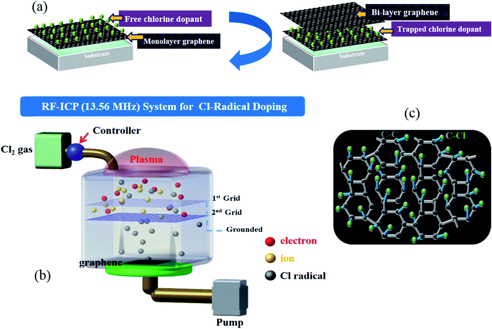 | ||
| Fig. 1 (a) The strategy of Cl-trap doping on layer-by-layer graphene using the ICP system. (b) The low damage ICP source used in the present study, which is comprised of a dual mesh assembly inserted between the source and substrate. (c) An image of the crystal structure of chlorinated graphene with covalent C–Cl bonding. | ||
To observe the low energy Cl adsorption on the graphene surface and interface, TEM analysis was utilized. Fig. 2(a) and (b) show the DF-TEM images of a bi-layer graphene without/with Cl trap-doping. The white-colored clouds shown in Fig. 2(b) are believed to be the Cl atom locations caused by trap doping between the graphene layers. A thin network of white color is also shown in Fig. 2(a), which is believed to be the slight Cl-doping originating from the FeCl3 etchant. The existence of Cl atoms was also proven by micro-EDS in TEM with the analysis points confirming that the Cl adsorbates were small (0.5%) and that they were sandwiched between two graphene layers, as shown in Fig. 2(c). In Fig. 2(c), the oxygen composition was increased from 0.96% (pristine bi-layer graphene) to 3.27% (Cl-trapped bi-layer graphene) because all our experiments were carried out in an air atmosphere; in addition, the layer-by-layer graphene transfer was via wet method (PMMA). Therefore, reactions occur between the experimental processes with the contaminants, impurities in the air or the residues during wet transfer and these contaminants or residues contain oxygen functional groups (OH–, COOH–, etc.), which are known as key factor in the deterioration of device performance. As the result, residues and impurities are inevitable during the CVD process of graphene, even a little bit. This is still a big challenge for 2D-materials research community. Recently, a promising method using the direct-growth of graphene on insulating substrates to avoid the wet transfer process was revealed and is still in progress.31
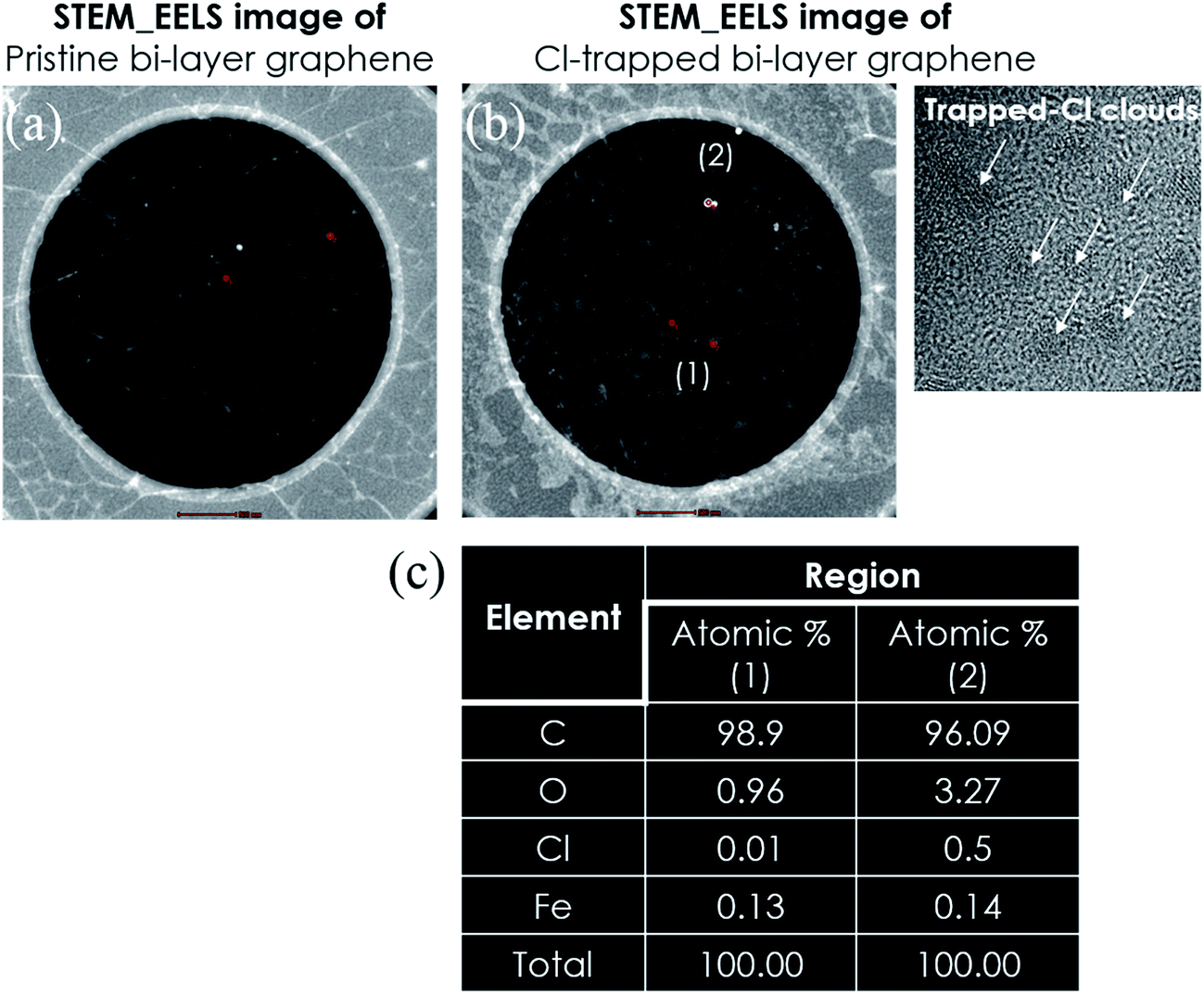 | ||
| Fig. 2 TEM images (a and b) of pristine bi-layer graphene and the Cl-trapped bi-layer graphene. (c) Micro-EDS data of the atomic percentages in regions (1) and (2) of (b). | ||
The Raman and XPS investigations used in this study have been investigated in detail in our previous report.29 In addition, we also showed the Raman spectra of tri-layer graphene with/without p-type Cl-trap doping (see Fig. S1, ESI†). With Cl-trap doping, the tri-layer graphene showed the blue-right shift in the G and 2D peaks (1577 and 2679 cm−1) when compared with the G and 2D peaks in the without Cl-trap doping of tri-layer graphene (1574 and 2675 cm−1), indicating the Cl dopant as a p-type dopant on graphene. In other words, the Raman spectra showed a blue-shift of 3 cm−1 and 4 cm−1 in the G and 2D peaks, indicating the Cl dopant as a p-type dopant on graphene. In fact, an investigation of the blue-shifts in the peaks of the Raman spectra of few-layer graphene has been carried out in detail in previous reports.9,32
For the long-term stability testing of Cl trap-doping on graphene, a thermal annealing process was carried out (Fig. 3). In fact, we kept some of the doped graphene samples used for the experiment, which were made four months earlier and, therefore, the Rs values were re-measured. We found no change in the Rs values after exposure to an air environment for four months. The Rs values for 130 Ω sq−1 of bi-layer graphene and 72 Ω sq−1 of tri-layer graphene were measured. Moreover, the four-month-old-doped graphene samples were heated for 100 h in a vacuum furnace at 230 °C and, as shown in Fig. 3, no significant change in the Rs values was observed. Therefore, it is believed that the doped grapheme samples prepared in our study are extremely stable.
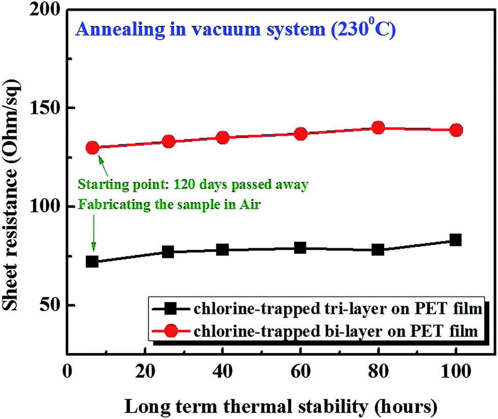 | ||
| Fig. 3 Thermal stability testing of the Cl-trapped bi-layer and tri-layer graphene in a vacuum furnace. | ||
Fig. 4(a) shows the Hall mobility values of the graphene samples without and with Cl-doping as a function of the Rs value. The Cl-doped mono-, bi-, tri-layer samples showed hole mobilities and Rs values of (2750 cm2 V−1 s−1, 305 Ω sq−1), (3352 cm2 V−1 s−1, 118 Ω sq−1), and (3970 cm2 V−1 s−1, 72 Ω sq−1), respectively. Due to the Cl p-type doping effect, these doped results are much higher when compared to those without Cl-doping.
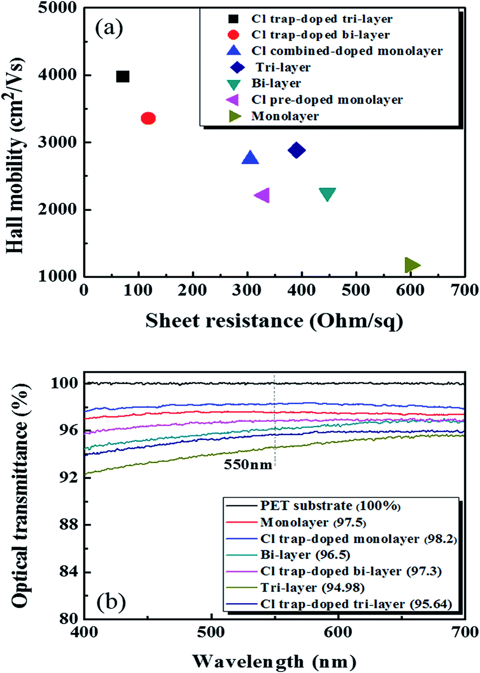 | ||
| Fig. 4 (a) The Hall mobility values of graphene with/without Cl-doping as a function of the sheet resistance. (b) The optical transmittance of the graphene samples with/without Cl-doping. | ||
The explanation of the mechanism of Cl p-type doping has been presented in detail in our previous report (with the strongly covalent C–Cl bonds in the graphene lattice).29 Due to the Cl p-type doping, the Rs value was decreased and led to an enhancement in the conductivity and Hall mobility of graphene. The correlations between the Rs value, conductivity and mobility are depicted in the formulas: Rs = ρL/A and ρ = 1/σ = 1/(enμ) where ρ is the resistivity, L is the length of the piece of graphene, A is the cross-sectional area of the specimen, σ is the conductivity, e is the electron, n is the carrier density, and μ is the mobility. In fact, these correlations have been well-described by De et al.33
The high % T of graphene layer and low Rs value are very important in transparent electrode-based applications. Pham et al. obtained the best values for Rs and % T in doped mono-layer graphene on a PET substrate at 240 Ω sq−1 and 97.7%, respectively.29 Therefore, we measured the % T of the mono-, bi-, and tri-layer graphene on PET doped with Cl plasma and the results are shown in Fig. 4(b). The monolayer graphene doped with the optimized doping process (90 s of pre-doping and 120 s of normal-doping) showed a high % T of ∼98.2% at 550 nm. For the bi-layer graphene and tri-layer graphene doped via cyclic trap doping using Cl plasma, we measured the % T at 97.3 and 95.64% at 550 nm, respectively. Because one monolayer graphene absorbs ∼2.3% at 550 nm (ref. 34) and the light excitation of Cl atoms,35–37 the % T of the doped mono- (98.2%), bi- (97.3%), and tri- (95.64%) layer graphene samples that we observed in the experiments were a little higher than those of the undoped pristine mono- (97.5%), bi- (96.5%), and tri-layer graphene (94.98%) samples.
Conclusions
In conclusion, we demonstrated the Cl-doping of graphene using an ICP system. Using TEM analysis, the Cl-trap doping strategy was generally formed well between the layer-by-layer graphene. Moreover, by thermal stability testing, the Cl-trapped layer-by-layer graphene showed a very high thermal stability in vacuum at 230 °C for 100 hours. We also obtained the Rs and % T of the Cl-trapped tri-layer graphene at 72 Ω sq−1 and 95.64% at 550 nm, respectively. In addition, high hole mobilities of the Cl-trapped bi- and tri-layer graphene samples of up to 3352 and 3970 cm2 V−1 s−1, respectively, were achieved. This study opens the promising potential for utilizing a combination of Cl pre-doping and normal-doping for transparent graphene electrode-based applications,38 e.g. OLEDs, photodetectors, sensor, and solar cells.Experimental
Cu foil with an area of 100 × 90 cm2 and thickness of 75 μm was rolled into a CVD vacuum chamber made of quartz. First, the discharge chamber was filled with H2 gas at the flow rate of 10 sccm and then the Cu foil was annealed for 1 h at 1050 °C under a H2 environment. Then, graphene was synthesized at 1050 °C under a H2/CH4 (10/20 sccm) environment for 30 min and then the chamber was cooled down to room temperature with H2 gas (10 sccm) for 1 h. After the synthesis, the Cu foil was cut into small equal pieces (3 × 3 cm2). These small pieces of graphene on Cu foil were affixed on glass substrates using tape and the glass substrate was used as a holder for the graphene–Cu foil assembly.An innovative ICP source, with dual mesh assembly inserted between source and substrate to prevent the bombardment of energetic ions on the graphene surface, has been demonstrated in a previous report.29 The Cl2 plasma was generated under the conditions of 13.56 MHz, 20 W, 10 mTorr, and 60 sccm for 90–120 s. The graphene films, which were inserted in the chamber, were cooled down to 15 °C using a chiller.
The Rs values of the graphene films on PET and SiO2 were measured utilizing an Rs meter (Dasoleng, FPP-2400). UV spectroscopy (Shimadzu, 3600) was used to measure the optical characteristics of the graphene films with/without Cl trap-doping. To observe the Cl atoms between the graphene layers, a micro-EDS (energy dispersive X-ray spectroscopy) installed in the DF (dark field)-TEM (Transmission Electron Microscopy, FEI Titan 80/300) and scanning transmission electron microscopy-electron energy loss spectroscopy (STEM-EELS) were utilized. The Hall carrier mobility was measured using a Hall effect measurement system (HMS-3000, ECOPIA). Raman spectroscopy (Renishaw, RM-1000 Invia) with an excitation energy of 2.41 eV (514 nm, Ar+ ion laser) was used for the characterization of the graphene film trapped with Cl radicals.
Acknowledgements
This research was supported by the Nano Material Technology Development Program through the National Research Foundation of Korea (NRF), funded by the Ministry of Education, Science and Technology (2016M3A7B4910429).Notes and references
- K. S. Novoselov, A. K. Geim, S. V. Morozov, D. Jiang, Y. Zhang, S. V. Dubonos, I. V. Grigorieva and A. Firsov, Science, 2004, 306, 666–669 CrossRef CAS PubMed.
- K. S. Novoselov, A. K. Geim, S. V. Morozov, D. Jiang, M. I. Katsnelson, I. V. Grigorieva, S. V. Dubonos and A. Firsov, Nature, 2005, 438, 197–200 CrossRef CAS PubMed.
- C. R. Dean, A. F. Young, C. Lee, L. Wang, S. Sorgenfrei and K. Watanabe, Nat. Nanotechnol., 2010, 5, 722–726 CrossRef CAS PubMed.
- D. W. Brenner, O. A. Shenderova, J. A. Harrison, J. S. Sttuart, B. Ni and S. B. Sinnott, J. Phys.: Condens. Matter, 2002, 14, 783–802 CrossRef CAS.
- C. Mattevi, H. W. Kim and M. Chhowalla, J. Mater. Chem., 2011, 21, 3324–3334 RSC.
- H. Liu, Y. Liu and D. Zhu, J. Mater. Chem., 2011, 21, 3335–3345 RSC.
- W. Chen, D. Qi, X. Gao and A. T. S. Wee, Prog. Surf. Sci., 2009, 84, 279–321 CrossRef CAS.
- S. M. Kim, A. Hsu, Y. H. Lee, M. Dresselhaus, T. Palacios, K. K. Kim and J. Kong, Nanotechnology, 2013, 24, 365602 CrossRef PubMed.
- F. Gunes, H. J. Shin, C. Biswas, G. H. Han, E. S. Kim, S. J. Chae, J. Y. Choi and Y. H. Lee, ACS Nano, 2010, 4, 4595–4600 CrossRef CAS PubMed.
- J. Zheng, H. T. Liu, B. Wu, C. A. Di, Y. L. Guo, T. Wu, G. Yu, Y. Q. Liu and D. B. Zhu, Sci. Rep., 2012, 2, 662 Search PubMed.
- X. Zhang, A. Hsu, H. Wang, Y. Song, J. Kong, M. S. Dresselhaus and T. Palacios, ACS Nano, 2013, 7, 7262–7270 CrossRef CAS PubMed.
- J. Wu, L. Xie, Y. G. Li, H. L. Wang, Y. Ouyang, J. Guo and H. Dai, J. Am. Chem. Soc., 2011, 13, 19668–19671 CrossRef PubMed.
- B. Li, L. Zhou, D. Wu, H. Peng, K. Yan and Z. Liu, ACS Nano, 2011, 5, 5957–5961 CrossRef CAS PubMed.
- S. Tongay, K. Berke, M. Lemaitre, Z. Nasrollani, D. B. Tanner, A. F. Hebard and B. R. Appleton, Nanotechnology, 2011, 22, 425701 CrossRef CAS PubMed.
- N. Mcevoy, H. Nolan, N. A. Kumar, T. Hallam and G. S. Duesberg, Carbon, 2013, 54, 283–290 CrossRef CAS.
- N. Peltekis, S. Kumar, N. Mcevoy, K. Lee, A. Weidlich and G. S. Duesberg, Carbon, 2012, 50, 395–403 CrossRef CAS.
- P. Niranan, S. Marco, D. Alberto and A. Athanasia, J. Mater. Sci., 2011, 46, 5044–5049 CrossRef.
- L. Xuelei, A. S. Brent, C. Irene, C. Guangjun, A. H. Christina, Z. Qin, O. Yaw, Y. Kai, P. Hailin, L. Qiliang, Z. Xiaoxiao, Z. Hui, R. H. W. Angela, L. Zhongfan, M. P. Lian and A. R. Curt, ACS Nano, 2011, 5, 9144–9153 CrossRef PubMed.
- Y. F. Xiao, N. Ryo, C. Y. Li and T. Katsumi, Nanotechnology, 2010, 21, 475208 CrossRef PubMed.
- C. Stephen, R. K. Peter and J. R. Preston, J. Vac. Sci. Technol., B: Microelectron. Nanometer Struct.--Process., Meas., Phenom., 1996, 14, 4129–4133 CrossRef.
- A. M. Goosens, V. E. Calado, A. Barreiro, K. Watanabe, T. Taniguchi and L. M. K. Vandersypen, Appl. Phys. Lett., 2012, 100, 073110 CrossRef.
- C. L. Yung, C. L. Chun, H. Y. Chao, J. Chuanhong, S. Kazu and W. C. Po, Nano Lett., 2012, 12, 414–419 CrossRef PubMed.
- S. L. Wei, T. N. Chang and T. L. T. John, Nano Lett., 2014, 14, 3840–3847 CrossRef PubMed.
- J. Moser, A. Barreiro and A. Batchtold, Appl. Phys. Lett., 2007, 91, 163513 CrossRef.
- H. Micheal, B. Ryan and N. Lukas, Phys. Lett. A, 2013, 377, 1455–1458 CrossRef.
- H. Terrones, R. Lv, M. Terrones and M. Dresselhaus, Rep. Prog. Phys., 2012, 75, 062501 CrossRef PubMed.
- D. L. Duong, G. H. Han, S. M. Lee, F. Gunes, E. S. Kim, S. T. Kim, Q. H. Ta, K. P. So, S. J. Yoon, S. J. Chae, Y. W. Jo, M. H. Park, S. H. Chae, S. C. Lim, J. Y. Choi and Y. H. Lee, Nature, 2012, 490, 235–239 CrossRef CAS PubMed.
- G. H. Han, F. Gunes, J. J. Bae, E. S. Kim, S. J. Chae, H. J. Shin, J. Y. Choi, D. Pribat and Y. H. Lee, Nano Lett., 2011, 11, 4144–4148 CrossRef CAS PubMed.
- V. P. Pham, K. H. Kim, M. H. Jeon, S. H. Lee, K. N. Kim and G. Y. Yeom, Carbon, 2015, 95, 664–671 CrossRef CAS.
- D. W. Brenner, O. A. Shenderova, J. A. Harrison, J. S. Sttuart, B. Ni and S. B. Sinnott, J. Phys.: Condens. Matter, 2002, 14, 783 CrossRef CAS.
- H. Wang and G. Yu, Adv. Mater., 2016, 28, 4956–4975 CrossRef CAS PubMed.
- M. Chen, H. Zhou, C. Qiu, H. Yang, F. Yu and L. Sun, Nanotechnology, 2012, 23, 115706 CrossRef PubMed.
- S. De and J. Coleman, ACS Nano, 2010, 4, 2713–2720 CrossRef CAS PubMed.
- R. R. Nair, P. Blake, A. N. Grigorenko, K. S. Novoselov, T. J. Booth, T. Stauber, N. M. R. Peres and A. K. Geim, Science, 2008, 320, 1308 CrossRef CAS PubMed.
- K. Suzuki, I. Nishiyama, Y. Ozaki and K. Kuchitsu, Chem. Phys. Lett., 1978, 58, 145–148 CrossRef CAS.
- J. B. Nee, Chin. J. Phys., 1988, 26, 254–261 CAS.
- H. A. Bechtel, J. P. Canden, D. J. A. Brown, M. R. Martin, R. N. Zare and K. Vodopyanov, Angew. Chem., Int. Ed., 2005, 44, 2382–2385 CrossRef CAS PubMed.
- D. A. C. Brownson and C. Banks, Phys. Chem. Chem. Phys., 2012, 14, 8264–8281 RSC.
Footnote |
| † Electronic supplementary information (ESI) available. See DOI: 10.1039/c7ra01330b |
| This journal is © The Royal Society of Chemistry 2017 |