
 Open Access Article
 This Open Access Article is licensed under a Creative Commons Attribution-Non Commercial 3.0 Unported Licence
Fabrication of functional 3D multi-level microstructures on transparent substrates by one step back-side UV photolithography
Myeongwoo Kanga,
Jae Hwan Byunb,
Sangcheol Na ac and
Noo Li Jeon*abc
ac and
Noo Li Jeon*abc
aDivision of WCU Multiscale Mechanical Design, Seoul National University, Seoul, 151-744, Korea. E-mail: njeon@snu.ac.kr; Fax: +82-2-880-7119; Tel: +82-2-880-7111
bSchool of Mechanical and Aerospace Engineering, Seoul National University, Seoul, 151-744, Korea
cInstitute of Advanced Machinery and Design (SNU-IAMD), Seoul National University, Seoul, 151-744, Korea
First published on 27th February 2017
Abstract
This paper describes simple photolithography-based methods to fabricate multi-level three-dimensional (3D) microstructures without repeated processes using flexible and transparent film substrates such as polyethylene terephthalate (PET). When using a thin transparent film substrate, propagation of UV can be assumed to be near-field diffraction where wave property is more dominant than particle property. Using this phenomena, we patterned multi-level 3D SU-8 microstructures such as master molds for microfluidic neuron culture devices. PET film is compatible with SU-8 photoresist processing steps and exhibited good adhesion with patterned structures that were stable for more than 50 replica moldings. Advantages of the suggested method using PET are (1) simplified and faster fabrication of 3D structures with tunable thickness, (2) no requirement for mask alignment and repeated processes in fabricating multilayer structure, and (3) economical process with substrates that are ∼1000 times cheaper than Si wafers. To use PET based molds for soft lithography, we have designed an isothermal curing jig for replica molding with PDMS. Use of the PET substrate combined with back-side exposure can dramatically reduce fabrication time and cost. We believe that PET films can replace expensive Si based wafers for soft lithography master fabrication. Furthermore, they can be applied to the fabrication of microfluidic devices and complex multi-level high aspect ratio structures as an alternative to conventional photolithography.
1. Introduction
There are many photolithography-based methods that have been employed to produce 3D microstructures for MEMS applications. LIGA processing was developed to fabricate high aspect ratio structures by combining X-ray lithography and electroplating.1 Other examples include slanted structures generated by inclined photolithography,2 and bell-shaped structures fabricated using back-side exposure techniques.3 Micro-needle structures with different heights were fabricated using partial crosslinking of the photoresist based on back-side exposure.4 In addition, grey scale lithography was developed to make multi-level and slanted structures with one mask.5,6 Although these methods are novel and powerful techniques to fabricate various micro/nano structures they require special facilities such as an X-ray source or other special equipment that increases their complexity.Microfluidics-based devices have several advantages over conventional large-scale analytical process because they offer faster and more sensitive detection with smaller reagent volume. Microfluidic technology enables the integration of an entire laboratory on a single chip.7,8 For advanced lab-on-a-chip operations, microfluidic devices may require complex 3D structures that can integrate various functions, such as mixer, fluidic isolation channel, and valves.9 Microfluidic approaches are being increasingly used in performing cell-based assays and other applications. For example, to achieve fluidic isolation between compartments in neuron culture device, double layer, aligned SU-8 process was developed.10,11
Photolithography is the most common fabrication technique used for making master mold for microfluidic devices (MFDs)12,13 and soft lithography method is widely used to fabricate PDMS-based devices. To realize multi-level structures, photolithography process is performed repeatedly with alignment after each steps.4,14,15 Although conventional multilayer photolithography technique for fabricating master molds has many advantages, it uses expensive substrates (i.e. Si wafers at $ 20 per wafer) and take long and cumbersome processing steps that require multiple mask alignments.
This paper describes an unconventional method to fabricate functional multi-level structures in one step. Fabrication of master mold for soft lithography usually require many rounds of optimization. We wanted to develop a simple and rapid method for fabricating multi-level structures with taking advantages of PET films (outstanding cost and physical properties). In this paper, compatibility of PET film was first verified as an alternative substrate material for SU-8 patterning process (adhesion, temperature and chemical resistance). Using PET film substrate, we patterned multi-level structures with new photolithography method based on back side UV exposure. The heights of the structures were controlled by changing the slit widths to control the UV diffraction. Due to the thin substrate, near-field diffraction assumption was adopted and mathematically analyzed to predict the shape and intensity of the diffracted UV. Simulated the Fresnel diffraction model estimated the UV intensity distribution pattern as a function of slit width. On consideration the diffraction property of backside lithography, multi-level and slanted structures are fabricated with single UV exposure.
In this study, we describes applications using one step multi-level structure patterning. We fabricated two layer integrated structure to make microfluidic neuron culture device with single photolithography step without mask alignment. For the convenience soft lithography, curing jig was developed considering the uniformity of heat transfer.
2. Materials and methods
2.1 Photoresist patterning on PET film
We patterned multi-level photoresist structures on PET substrate. In this study, SU-8 50 and 100 (MicroChem, Newton, MA) photoresists were used. SU-8 is a widely used negative-tone photoresist for MEMS and microfluidics microfabrication. SU-8 contains bisphenol A novolac epoxy oligomer for cross-linking and triarylsulfonium hexafluoroantimonate salt as a photoacid generator.16 UV irradiation initiates generating a low concentration of a strong acid hexafluoroantimonic acid which crosslinks SU-8. Dose of the UV light must be sufficiently high to initiate crosslinking. Minimum critical exposure dose to initiate polymerization for SU-8 is 49.4 ± 3.9 mJ cm−2.17 The crosslinking of SU-8 begins at the exposed surface proximal to the UV light.We used commercially available PET film (Over Head Projection Film, 3M, MN) as an alternative substrate. The thickness of PET film is approximately 130 μm. The glass transition temperature is 140 °C, which is significantly higher than the highest temperature used for process SU-8 for photolithography (pre and post exposure bake@95 °C). PET film has excellent chemical resistance; it is not degraded or dissolved by the organic solvents including SU-8 developer. In this study, we used AZ1500 Thinner (AZ Electronic Materials, South Korea) as SU-8 developer. The adhesion between SU-8 and PET film is also notably strong with silicon wafers. In addition, PET is very cost-effective material whose cost is almost 1000 times lower than that of silicon wafers. The PET films were cut to 4 in. diameter circular shape using cutting plotter (Craft ROBO, Graphtech, US). Before using, PET substrates were cleaned with small amount of developer and dried with nitrogen blower.
After substrate preparation, SU-8 50 and 100 were applied on PET film substrates with appropriate thickness by spin coating. Spin speeds were 1000 rpm for 250 μm of SU-8 100 and 1250 rpm for 80 μm of SU-8 50. To rid the solvent in the cast SU-8 film, coated substrate was placed on a hot plate the temperature was increased from 65 °C to 95 °C. Ramping the hot plate temperature from 65 °C is important in obtaining good adhesion between SU-8 and PET substrate. An UV aligner (Shinu MST, South Korea) with i-line filter was used for exposure. Depending on method, transparency masks were placed under the PET substrate or above. The intensity of UV was 10 mW cm−2 and exposure time was controlled to obtain 3D structures to obtain specific thickness of photoresist layer. Post exposure bake at 95 °C was performed to finish cross-linking of the photoresist. The three dimensional SU-8 microstructures can be obtained after development.
2.2 Microfluidic device fabrication
MFDs were fabricated using soft lithography and rapid prototyping. Master molds were fabricated by patterning SU-8 photoresist on transparent PET film substrates. Positive replicas were fabricated by molding polydimethylsiloxane (PDMS, Sylgard 184, Dow Corning, Midland, MI) against the master. The cured PDMS was peeled off, and holes were punched (with sharpened needles) for use as reservoirs or fluidic interconnects. The PDMS was irreversibly bonded to a glass slide upon treatment of both with an air-plasma generator (Femto Science, South Korea), thereby forming the MFD.18,19 After bonding, the device was filled with poly-D-lysine (PDL) solution for surface treatment. The PDL was washed and exchanged for culture medium 1 day before cell plating.2.3 Cell preparation
Animals were maintained in accordance with the guidelines of the Institute of Laboratory Animal Resources (ILAR) at Seoul National University, Korea, and approved by the Institutional Animal Care and Use Committees (IACUC) of Seoul National University. Primary cortical neurons were prepared from embryonic Sprague-Dawley rats (TP18) following the anatomic procedure. Six cortices were dissected from extracted brain in 1× Hank's balanced salt solution (HBSS) and treated with 3 mL of 0.125% trypsin/ethylenediaminetetraacetic acid (EDTA) for 15 min in a 37 °C water bath. The trypsin/EDTA was removed by rinsing three times with HBSS; then, and 1 mL of the plating medium [Dulbecco's Modified Eagle Medium (DMEM) with 10% fetal bovine solution (FBS) and 5000 units per mL of penicillin–streptomycin (Pen/Strep) solution] was added, and the mixture was centrifuged for 1 min at 1100 rpm. The supernatant was then discarded, and 2 mL of neurobasal medium containing 2% of supplement B-27, 0.25% GlutaMax media supplement, and 1% Pen/Strep (Invitrogen, Carlsbad, CA) was added. The cells were triturated using a Pasteur pipette. The cell suspension was filtered through a cell strainer with a pore size of 22 μm, and cell viability and density were determined by trypan blue staining. Cell density was adjusted to 6 × 10⁶ cells per milliliter. Before loading the cells, sufficient medium to keep the glass slide wet was aspirated from the prepared device. For each device, 20 μL was loaded onto only the soma side of the channel. The devices were incubated for 15 min to allow the neurons to stick to the PDL-treated glass slides before additional medium was added. Medium was changed every other day.203. Result and discussion
3.1 SU-8 patterning on the PET film by conventional photolithography
Fig. 1 shows the photoresist patterning on PET film; as seen in the figure, the quality of the pattern is well defined compared with the silicon master. Various SU-8 micro-structures were successfully patterned on PET film. To verify the quality of the SU-8 patterning, as Fig. 1C and D, we patterned circular and rectangular patterns whose sizes varied from 20 to 100 μm with 20 μm-heights, and also complex and long structures of 10 μm-heights were fabricated without failure. | ||
| Fig. 1 Photoresist pattern on PET film substrate. (A) Microscale negative tone photoresist (SU-8) structures are patterned on PET film substrate by conventional photolithography method. (B) Patterns with various structures have been successfully patterned on PET substrate. (C) Microstructures are fabricated with features as small as 10 μm. Patterned photoresists exhibit good adhesion with PET film substrate withstanding over 45 times of tape peel tests and 40 times of PDMS replica demolding, respectively. (D) Extremely long structures whose length is more than 500 μm are successfully patterned without failure. (E) PDMS microfluidic device has been replicated from PET based master fabricated by two layer photolithography. Microstructures have different heights (5 μm and 100 μm) and it makes fluidic isolation between channels. | ||
During the fabrication processes, PET film showed fine properties as a substrate. SU-8 was well coated on PET film without any chemical assistances, and coating thickness was same as typical coating using Si based wafers. Also it was not deformed or melted by hot environments and solvent.
To check durability of fabricated PET as the master mold for microfluidic devices, we tested the adhesion between SU-8 and the PET film using Scotch tape and PDMS replication. The patterns maintained their shape and position during attaching and detaching Scotch tape more than 45 times and 40 times of demolding PDMS.
As the Fig. 1E, PDMS microfluidic devices was replicated from PET based master. Multi-level SU-8 microstructures were well defined and PDMS devices were replicated SU-8 structures. The surface of PDMS replica is clean enough to bonded with cover glass and the performance of device was same as conventional device.
3.2 UV distribution in photoresist during backside exposure
Backside photolithography technique has an advantage to fabricate high aspect ratio microstructures because inverted incident UV light minimizes “big head effect” in conventional photolithography. Thus, backside photolithography has been used to fabricate high aspect ratio structures such as microneedles and microlenses.1,20 Nevertheless the advantage of backside photolithography, UV diffraction problem should be considered because UV light distribution and diffraction phenomenon can be occurred along the gap of mask plane and UV image screen plane, i.e. photoresist. Basically, shape of light distribution, i.e. diffraction and/or interference is determined by various optical and spatial parameters. Wave length, curvature of wave front, numbers of source are the essential optical parameters and spatial parameters, e.g. distance between light source, slit and image screen, the shape, area and number of slits play a critical role for the light distribution on screen.21 Moreover, some of material property such as absorption coefficient of UV should be considered to estimate the final light intensity distribution on photoresist.Light distribution, especially diffraction through slit can be classified into far- and near-field diffraction. In a view point of wave equation, far- and near-field diffraction is determined according to the underlying wave property of whether it shows feature of straight or wave, respectively. In addition, a concept of slit is ambiguous in optics, however we can estimate a slit works as like “slit” or “mask” depending on the relation of slit size and wavelength.
Many researchers have solved this light distribution problem in backside photolithography technique.4,22–24 Recently, a 3D model based on the Fresnel–Kirchhoff diffraction theory is presented to predict the sidewall profile of high aspect ratio structure using backside lithography with thick quarts glass substrate.25 Based on the distribution of UV light through slit, we designed a 3D multi-level fabrication technique by one step backside UV photolithography. In this study, we fabricated neuron device which has two different height of structure.7,26 One-step 3D multi-level lithography technique in this paper, however, uses PET film of which thickness is 130 μm. In our case, some of assumption is needed like below
(a) UV light of 365 nm is a plane wave because it passed through condenser before coming mask plane.
(b) Fresnel diffraction will dominantly occur by a practical rule-of-thumb of R < a2/λUV.21 Where R is the distance from mask plane to image screen, and a is a width of slit.
(c) According to above the rule-of-thumb, main channel part of neuron device works as just mask, thus its overall shape on photomask will be patterned on photoresist. However slight fringing around its periphery should occur due to local diffraction along the edge of mask.
The light amplitude at point P of image screen is:
 | (1) |
Here, the terms in the bracket of right hand side represents the obliquity factor and it calibrates intensity of distributed light on screen. The obliquity factor and the radius factor 1/rr′ can be considered as constant in integral because those change sufficiently slower than eik(r+r′), thus eqn (1) is written finally as
 | (2) |
Here, U0 is the UV intensity of source and r,r′ is the distance from source to arbitrary point on slit Q and Q to the point P, respectively.
Following the usual form of derivation, eqn (2) is introduced using the dimensionless variables u and v defined by
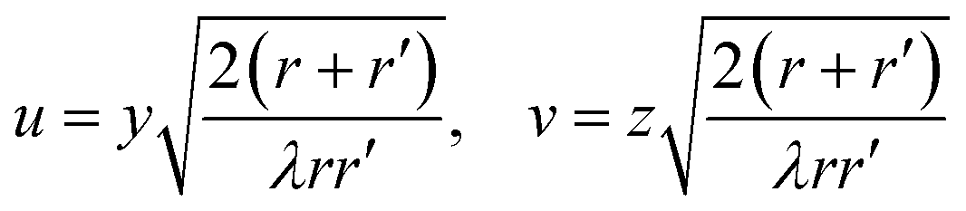 | (3) |
Substituting eqn (3) into eqn (2) and utilizing the dimensionless variables,
 | (4) |
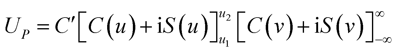
Each integral of eqn (4) composed of separated real and imaginary part of Fresnel integral:
 | (5) |
Assuming that the height of microgrooves for axon tunnel can be formed as semi-infinite slit because the width is below 10 μm, and then the length is longer than several hundred times. Consequently, the light amplitude eqn (5) is expressed simply by letting v1 = −∞, v2 = ∞.
 | (6) |
 | (7) |
The light intensity at the point P is written as
| IP = UPŨP/2 × e−αPETT × e−αSU-8h |
Fig. 2F shows mathematically simulated intensity profile of diffracted UV based on eqn (7) and IP using Matlab. As the figure, diffracted UV intensity fluctuates along the longitudinal direction.
3.3 UV exposure through slit patterns
Light diffraction occurs when a wave encounters an obstacle. According to the Huygens–Fresnel principle, light is diffracted and focused after passing through a thin slit. As the width of the slit is increased, the dose of penetrating light will increase. In this study, we used 365 nm UV light. Fig. 2A shows the UV penetration test method. For the transparency mask, we used a printed film mask with various slit patterns to determine the amount of penetrated UV light according to the slit width. The widths of the slits varied from 10 to 150 μm. The PET film was used as the substrate and SU-8 was coated at a 250 μm thickness. The transparency mask, which had 15 slits, was placed on the backside of the coated film. After mask alignment, the backside of the film was exposed to UV light at doses of 50, 100, 150, 200, 250 and 300 mJ cm−2. The heights of the structures were measured to evaluate the variation of the diffracted UV light.20 Fig. 2B shows that the heights of the crosslinked SU-8 structure were increased when either the slit width or the UV energy was increased. Unlike typical photolithography, the cross section of SU-8 crosslinked by backside UV exposure is triangular the shape of diffracted light. In conventional front-side photolithography, UV light passes through only one medium (air) before reaching the photoresist and result in perpendicular profile if given enough exposure dose. In our experiments, light reaching the photoresist must pass through the transparent PET film substrate. The presence of additional medium and its thickness perturb the direction of light path. Lee, et al. reported creation of different shapes microstructures when various medium is inserted in the light path.27 The cross section of the structures formed are greatly influenced by the nature of the medium in the light path. A notable feature is that the 70 μm width is threshold width to saturate penetrated UV, i.e. if the slit width is bigger than 70 μm, UV light saturated due to the high attenuation of SU-8 and height of crosslinked SU-8 is not proportional to the slit width. The SEM images of Fig. 2C shows the cross section of crosslinked SU-8. As the Fig. 2C, triangular cross section changes to trapezoidal when the slit is wider than 70 μm. Fig. 2D is DSLR image of multi-level SU-8 structures on PET substrate fabricated with complex patterned mask. The height of structures continuously varies according to the pattern size. The SEM image on Fig. 2E shows periodic height variation along the longitudinal direction and it is same aspect as the simulation result on Fig. 2F. | ||
| Fig. 2 Back-side exposure for obtaining height controlled line-structure with varying slit width and UV dose. (A) Schematic of back-side exposure. Transparency mask is placed below the SU-8 (250 μm) coated PET substrate. A mask with slit patterns of varying width were used to obtain varying thickness of cross-linked SU-8. Wider slits resulted in thicker cross-linked SU-8 layer. (B) As the graphs indicate, at constant UV dose, cross-linked height changes gradually increases for slit widths to 70 μm and show maximum crosslinked thickness over 70 μm slit width. Similar to width control case, the maximum cross-linked thickness increases linearly for 50 mJ cm−2 to 300 mJ cm−2, respectively. (C) The SEM images according to various slit width for 250 mJ cm−2 of UV. Fabricated structures have triangular cross sections before 70 μm and it turns to trapezoidal cross section after 70 μm. Slit width become wide toward right by 10 μm step. (D) DSLR image of multi-level microstructure fabricated by backside exposure. The heights of structures vary according to the mask patterns. (E) Triangular structures have periodic height variation along the longitudinal direction. (F) Intensity distribution along the longitudinal direction according to the Fresnel diffraction. Intensity profile was simulated by Matlab. | ||
Using this characteristic, 20 μm to 120 μm height structures can be fabricated with one UV exposure. We confirmed that we created multi-level structures using one exposure and various slit widths. Thus, we developed a new photolithography technique than can be used to reduce MFD fabrication cost and time.
3.4 One step multi-level 3D structure fabrication
Typical multilayer photolithography methods are costly and lengthy; they require the use of several masks combined with cumbersome mask alignment steps and repeated processing. To overcome these inconveniences, using PET film and backside exposure, we developed new fabrication method that reduced both the time and cost of fabrication. In this method, the substrate should be transparent; in our work, we used commercially available PET film as the substrate. At 365 nm wavelength, optical properties of PET film were measured and its transmissivity τPET is approximately 83% and αPET is 14.33 cm−1. Fig. 3 shows various multi-level SU-8 structures fabricated on PET substrate by backside photolithography. To obtain multi-level structures, 250 μm of SU-8 coated on PET film and transparency mask which contains various patterns placed on the backside of coated substrate. Proper dose of UV was exposed on the backside of substrate to achieve appropriate height. As Fig. 3A, the size of patterns should bigger than 50 μm to ensure complex structures like star-shaped structures. The edges of structures have wavy surface because the diffracted UV has intensity variation (Fig. 3B). Using backside photolithography on PET substrate, diamond-like structures which have slanted smooth edges can be easily fabricated without size error. Fig. 3E shows various diamond-shaped structures fabricated with same mask. As the dose of UV varies, only heights of structures vary and the size of structures are regular. Fig. 3F is human circulatory system mimicked structure as the application of the backside photolithography. The simplified human body structure contains organs, arteries and capillaries with different height. The heights of structures was controlled by width of transparency mask pattern. | ||
| Fig. 3 Various microstructure fabricated on PET substrate by backside exposure. (A) SEM image of various multi-level SU-8 microstructures obtained by backside UV exposure. (B) The structures have wavy sidewalls caused by diffraction of light. (C) SU-8 structures of various sizes over PET is stably maintained after 40 iterations of PDMS demolding. (D) 3D complex microstructures fabricated by backside exposure. (E) Diamond-like microstructure array according to scale of mask and UV dose. UV dose increases toward the bottom. In contrast to conventional photolithography technique, various slanted side-wall microstructures can be fabricated easily and quickly due to the light diffraction property. This kind of shape can be applied to a valve module in microfluidic device without such as complex reflow technique. (F) Simplified human body structure was fabricated to mimic circulatory system containing artery and capillary with different heights. UV exposure dose for all examples are 200 mJ cm−2, except for (E). | ||
3.5 Application of backside photolithography for microfluidics
As the application of backside photolithography, we fabricated existing useful structures for microfluidics. In this study, we fabricated the mold for a microfluidic neuron culture device where thin microgrooves are needed to fluidically isolate axons from cell bodies.28 The standard neuron device contained multi-level structures with heights of 10 and 80 μm (same pattern dimension as the one used for conventional fabrication). Fig. 4A shows the fabrication process used to produce 3D SU-8 structures on a single SU-8 layer. First, the PET film was coated with a 80 μm layer of SU-8 which is the maximum height at 200 mJ cm−2; the coated substrate was then soft-baked to remove the solvent. After soft baking, we placed a transparency mask on backside of the substrate. In this method, only one transparency mask is required; this can be used to fabricate the total pattern, considering the 3D structures of differing heights. Specifically, heights of the 3D structures were controlled by adjusting the width of the mask pattern and the UV exposure dose. In accordance to light distribution phenomenon, two different height of microstructure is fabricated beneath the “slit” and “mask” region, respectively. The width of small patterns were 10 μm for 10 μm height structures and 1–5 mm for 80 μm height structures. After placing the transparency mask, the backside of the PET film was exposed to 200 mJ cm−2 UV. Next, the SU-8 was fully cured by placing the UV exposed substrate on a 95 °C hot plate for 20 min. After post exposure bake, the final pattern was developed. Using this method, we produced multi level 3D SU-8 microstructures by one-step backside UV exposure. We demonstrated production of complicated multi-level structures with various heights and widths. Using UV diffraction, we controlled the height of the structures by changing the pattern width of the transparency mask. As shown in Fig. 4B, the multi-level microstructures were successfully fabricated by one-step. As the figure, the surface and edges of the patterned SU-8 were rough and slanted due to partial cross-linking and light diffraction. Rough surface could be a problem for imaging; however, this can be overcome using a high-resolution lens or fluorescence tagging. Fig. 4C shows the photograph of the completed neuron device after bonding to a glass cover slip. Similar to the conventionally fabricated devices, fluidic isolation is achieved between the green dye filled soma chamber and red dye filled axon chambers. Fig. 4D shows the neurons stained with calcein AM for visualization of live neurons and their axons and dendrites. Neurons can be isolated to left side although the groove heights are 10 μm because the channel cross-sections are triangular rather than rectangular. | ||
| Fig. 4 Fabrication of functional 3D multi-level microstructure by one step backside UV photolithography (A) a multi-level pattern can be fabricated in a single step. Transparency mask is placed on the backside of SU-8 (80 μm) coated PET substrate. The transparency mask includes both micrometer scale patterns and millimeter scale patterns to obtain multi-level structures. Single exposure (200 mJ cm−2) with the mask placed under the SU-8 coated substrate resulted in pattern shown in (B). (B) Scanning electron microscopy image of fabricated multi-level SU-8 structures on PET film. (C) Microfluidic neuron-culture device replicated from back-side exposure fabricated SU-8 master mold on PET film. (D) Fluorescence image of calcein AM stained cultured neurons in replicated PDMS microfluidic device after 7 DIV. | ||
This single-exposure method can fabricate multi level structures with one transparency mask on single SU-8 layer without mask alignment and repeated processes. This method reduce the fabrication cost and time. Table 1 summarize the comparison between typical multi layer photolithography and one step backside exposure method.
| Conventional 2 layer method | Single exposure back-side | |
|---|---|---|
| a Two layer SU-8 structure whose heights are 3 μm and 80 μm. | ||
| Substrate (cost/4 in. wafer) | Silicon ($ 20) | PET ($ 0.02) |
| Fabrication steps | 10 | 5 |
| Total time (hours) | 2.5 | 1 |
| Number of masks | 2 | 1 |
| Mask alignment | Difficult | Not required |
3.6 Jig for replica molding PDMS with PET film master
Unlike thick rigid substrates like Si wafers, PET film is only 130 μm thick and flexible material and its thermal expansion coefficient is different from SU-8; PET: 59.4 ppm K−1, SU-8: 52 ppm K−1, SU-8 patterned PET master was bent about 5 degrees after fabrication. To cast PDMS and replicate the structures, we designed and fabricated a jig to flatten the PET films and to enhance removal after curing. Fig. 5A and B shows the photographs of the components and the assembled jig. Fig. 5C shows the exploded view of the jig. The frame of the jig was made from 3 aluminum pieces that are held together with 4 screws at each corner. Aluminum conducts heat well and can be machined easily. The PET film master was placed on MDF (medium-density fibreboard) piece and the top Al piece was clamped to hold it. Vacuum was briefly applied from below the MDF to hold the PET film flat before pouring liquid PDMS. Porous nature of the MDF board distributed the suction force uniformly across the PET such that they do not detach or curl up during PDMS processing. A one-way check valve placed on the vacuum line allowed untethered placement of the jig on a hot plate or in an oven. The function Teflon ring placed inside around the edge of the top plate was to match the thermal conductivity of MDF board so that a uniform thickness PDMS piece can be fabricated. When aluminum piece was used without the Teflon ring, due to high thermal conductivity, edges solidified before the bulk PDMS resulting in a piece with thick edges. An additional benefit of the Teflon is that due to poor adhesion with PDMS, demolding cured PDMS pieces is simplified without cutting. | ||
| Fig. 5 Design of the jig for replica molding with PET film master. Photographs of the (A) components and (B) the assembled jig. (C) Cross-section exploded view of the jig show three aluminum blocks that form the frame of the holder that are held together with 4 screws. Patterned PET film is placed on top of MDF (Medium-Density Fibreboard) board that is placed above silicone rubber gasket and vacuum manifold. Teflon ring was inserted between Al block and PDMS area to minimize thermal conductivity mismatch. The bottom aluminum alloy block is designed for applying vacuum to flatten the film masters and hold them flat on MDF surface (porous nature of MDF act as a “chuck” and distribute vacuum uniformly across the entire film). | ||
4. Conclusion
This paper mainly focus on alternative substrate material for photolithography and quick multi-level fabrication process in terms of economic feasibility and use convenience. In a view point of economics, we suggested PET film as an alternative substrate for photolithography. Chemical and physical characteristics, e.g. adhesion force with photoresist, chemical resistance and melting point, of PET film are enough to substitute the typical Si based wafers. Moreover, PET film is markedly 1000 times cheaper than those based on the 4-inches wafer area and flexible PET is free from crack and mechanical spalling. Therefore PET film has latent potential to replace the Si based wafers and it is especially useful to make prototype master mold using SU-8 photolithography.In use convenience of quick fabrication technique, we demonstrated simplified fabrication approach for 3D SU-8 microstructures on PET films using back-side UV exposure. Prior to backside lithography, mathematical approach is taken for simulating UV light distribution through PET and we predicted periodical fringing phenomenon of top and edge by near field diffraction dominant condition. Furthermore, the height of microstructure is able to be controlled linearly under slit scale of 70 μm due to the intensity reduction phenomenon and 3D shape also depends on the UV dose and slit width. Building on these results, we present the new method to fabricate multi-level microstructures on a single SU-8 layer with one photomask including total structure considered the heights and single backside UV exposure. This one step technique results in dramatically reduced fabrication time and cost and facilitates the manufacture of more complex structures that are difficult to make using conventional fabrication methods. In addition, we have developed the PDMS curing jig which forms spatial isothermal environment and it is helpful to improve curing throughput and durability of PET master.
Photolithography using flexible and transparent PET film has various potentialities on either biochips or others. In addition to SU-8, a variety of polymer can be coated on to PET. And PET is advantageous for large area fabrication which expand beyond the size of commercial Si based wafers, even it has possibility of roll-to-roll process for mass production.
Acknowledgements
This work was supported by the National Research Foundation of Korea (NRF) grant funded by the Korea government (MSIP) (No. NRF-2015R1A2A1A09005662, NRF-2016R1A4A1010796).References
- H. Sato, Y. Houshi and S. Shoji, Microsyst. Technol., 2004, 10, 440–443 CrossRef CAS.
- N. Futai, W. Gu and S. Takayama, Adv. Mater., 2004, 16, 1320–1323 CrossRef CAS.
- J. D. Rogers, A. H. O. Karkkainen, T. Tkaczyk, J. T. Rantala and M. R. Descour, Opt. Express, 2004, 12, 1294–1303 CrossRef PubMed.
- S. W. Lee and S. S. Lee, Opt. Lett., 2008, 33, 40–42 CrossRef PubMed.
- D. Qin, Y. Xia and G. M. Whitesides, Nat. Protoc., 2010, 5, 491–502 CrossRef CAS PubMed.
- D. Dendukuri, D. C. Pregibon, J. Collins, T. A. Hatton and P. S. Doyle, Nat. Mater., 2006, 5, 365–369 CrossRef CAS PubMed.
- S. W. Rhee, A. M. Taylor, C. H. Tu, D. H. Cribbs, C. W. Cotman and N. L. Jeon, Lab Chip, 2005, 5, 102–107 RSC.
- D. J. Beebe, G. A. Mensing and G. M. Walker, Annu. Rev. Biomed. Eng., 2002, 4, 261–286 CrossRef CAS PubMed.
- H. Andersson and A. Van den Berg, Sens. Actuators, B, 2003, 92, 315–325 CrossRef CAS.
- J. W. Park, B. Vahidi, A. M. Taylor, S. W. Rhee and N. L. Jeon, Nat. Protoc., 2006, 1, 2128–2136 CrossRef CAS PubMed.
- A. M. Taylor, M. Blurton-Jones, S. W. Rhee, D. H. Cribbs, C. W. Cotman and N. L. Jeon, Nat. Methods, 2005, 2, 599–605 CrossRef CAS PubMed.
- G. M. Whitesides, E. Ostuni, S. Takayama, X. Jiang and D. E. Ingber, Annu. Rev. Biomed. Eng., 2001, 3, 335–373 CrossRef CAS PubMed.
- Y. Xia and G. M. Whitesides, Annu. Rev. Mater. Sci., 1998, 28, 153–184 CrossRef CAS.
- A. Mata, A. J. Fleischman and S. Roy, J. Micromech. Microeng., 2006, 16, 276–284 CrossRef.
- C. Chen, D. Hirdes and A. Folch, Proc. Natl. Acad. Sci. U. S. A., 2003, 100, 1499 CrossRef CAS PubMed.
- A. del Campo and C. Greiner, J. Micromech. Microeng., 2007, 17, R81–R95 CrossRef CAS.
- W. H. Teh, U. Durig, U. Drechsler, C. G. Smith and H. J. Guntherodt, J. Appl. Phys., 2005, 97, 054907 CrossRef.
- D. B. Wolfe, D. Qin and G. M. Whitesides, Methods Mol. Biol., 2010, 583, 81–107 CAS.
- S. B. Dunnett and A. Björklund, Brain Res. Protoc., 1997, 1, 91–99 CrossRef CAS PubMed.
- H. Huang, W. Yang, T. Wang, T. Chuang and C. Fu, J. Micromech. Microeng., 2007, 17, 291–296 CrossRef CAS.
- E. Hecht, Optics, Addison Wesley, 4th edn, 2002 Search PubMed.
- H. Huang and C. Fu, J. Micromech. Microeng., 2007, 17, 393–402 CrossRef.
- K. M. Abedin and S. M. M. Rahman, Opt. Laser Technol., 2012, 44, 939–947 CrossRef.
- K. M. Abedin, M. R. Islam and A. F. M. Y. Haider, Opt. Laser Technol., 2007, 39, 237–246 CrossRef.
- W. C. Yang, Y. S. Huang, B. Y. Shew and C. C. Fu, J. Micromech. Microeng., 2013, 23, 035004 CrossRef.
- S. Na, M. Kang, S. Bang, D. Park, J. Kim, S. J. Sim, S. Chang and N. L. Jeon, Technology, 2016, 04, 240–248 CrossRef.
- J.-H. Lee, W.-S. Choi, K.-H. Lee and J.-B. Yoon, J. Micromech. Microeng., 2008, 18, 125015 CrossRef.
- A. M. Taylor, S. W. Rhee, C. H. Tu, D. H. Cribbs, C. W. Cotman and N. L. Jeon, Langmuir, 2003, 19, 1551–1556 CrossRef CAS PubMed.
| This journal is © The Royal Society of Chemistry 2017 |