
 Open Access Article
 This Open Access Article is licensed under a
 Creative Commons Attribution 3.0 Unported Licence
A self-powered solar-blind ultraviolet photodetector based on a Ag/ZnMgO/ZnO structure with fast response speed
Ming-Ming Fan ab,
Ke-Wei Liu*a,
Xing Chena,
Zhen-Zhong Zhanga,
Bing-Hui Lia and
De-Zhen Shen*a
ab,
Ke-Wei Liu*a,
Xing Chena,
Zhen-Zhong Zhanga,
Bing-Hui Lia and
De-Zhen Shen*a
aState Key Laboratory of Luminescence and Applications, Changchun Institute of Optics, Fine Mechanics and Physics, Chinese Academy of Sciences, Changchun 130033, People's Republic of China. E-mail: liukw@ciomp.ac.cn; shendz@ciomp.ac.cn
bCollege of Physics and Optoelectronics, Taiyuan University of Technology, Taiyuan 030024, People's Republic of China
First published on 24th February 2017
Abstract
A self-powered solar-blind ultraviolet (UV) photodetector was realized on a Ag/ZnMgO/ZnO vertical structure. A ZnO epitaxial layer was employed to serve as both the buffer layer for the growth of ZnMgO and the bottom electrode of the device. Interestingly, the device exhibited an obvious self-powered property owing to the built-in electric fields at the Ag/ZnMgO and ZnMgO/ZnO interfaces. At 0 V, the peak responsivity at 275 nm of our device was 16 mA W−1, which is comparable to that of other ZnMgO self-powered solar-blind UV photodetectors. Moreover, the device also exhibited a very fast response speed (24 μs rise time and 300 μs decay time) at 0 V. This study could provide a much easier and more feasible way to develop ZnMgO self-powered solar-blind UV photodetectors on foreign substrates with high responsivity, fast response speed, and low cost.
1. Introduction
Solar-blind ultraviolet (UV) photodetectors, working in the UV spectrum ranging from 220 nm to 280 nm with very high sensitivities, have drawn considerable attention due to their wide applications in commercial and military fields, such as in flame monitoring, missile warning, environmental monitoring, biological and chemical analysis, optical communication, and space research.1,2 Till now, a lot of solar-blind UV photodetectors have been demonstrated on wide band-gap semiconductors, such as GaAlN,3,4 β-Ga2O3,5,6 diamond,7,8 and ZnMgO.9–19 Among these candidates, ZnMgO alloys have been regarded as one of the most promising wide bandgap materials for solar-blind UV photodetection due to their excellent material properties, including lower density of defects, environmental friendliness, and stronger radiation hardness.20–22 In the past two decades, w-ZnMgO solar-blind UV photodetectors have been extensively studied by us and other groups.9–19Nowadays, energy-saving is a world-wide issue, and thus a photodetector without external power supply, usually known as a self-powered photodetector, is of significant importance for the practical application.2,23–28 As is well known, p–n junctions and Schottky junctions are the most common structures used as self-powered photodetectors, in which photogenerated electron–hole pairs can be separated by built-in electric field. However, p-type doping is still a big challenge for ZnO-based semiconductors, which hinders the further development of p–n homojunction photodetectors.20,22,29 Although self-powered UV photodetectors can be demonstrated by combining n-type ZnO-based materials with other p-type layers, such as Si,30,31 Cu2O,32 NiO,23,33 SiC,34,35 GaN,36,37 and organic materials,38,39 they are usually limited by the unexpected visible/IR response from p-type materials, the lattice-mismatched heteroepitaxy, or the instability of organic materials. Therefore, ZnMgO Schottky junction photodetector should be a suitable choice to realize self-powered solar-blind UV detection.
As is well known, ZnO is stabilized in the wurtzite structure (w), while MgO is stabilized in the cubic rock salt structure (c). As a result, the phase separation of w-ZnMgO alloy will occur with increasing the Mg content to extend its bandgap into solar-blind UV region.9 In order to resolve this problem and fabricate high Mg-content w-ZnMgO, the effective method is using ZnO substrates or buffer layers, and many w-ZnMgO solar-blind UV photodetectors have been demonstrated.10,11,14,15,19 However, most of these devices are based on metal–semiconductor–metal structure and very few information can be observed about w-ZnMgO Schottky junction solar-blind UV photodetectors. Endo, et al. reported a self-powered solar-blind UV device with a peak responsivity of 15 mA W−1 at 220 nm at 0 V on the basis of Pt/Zn0.41Mg0.59O Schottky photodetector on ZnO single-crystal substrate.19 However, the small size and expensive price of ZnO substrates limit the further development of this type of device.29 The growth of ZnO films on commercial foreign substrates may be an alternative route to solve this problem. Takagi, et al. have successfully fabricated single-phase w-ZnMgO with the bandgap in solar-blind UV region by using a ZnO buffer layer. However, the detailed information about its solar-blind UV detection behaviour and self-powered property cannot be found.15 In this study, w-ZnMgO was deposited on a-face Al2O3 (a-Al2O3) substrate due to its lattice mismatch to ZnO is as small as ∼2.4%.20 By introducing a ZnO buffer layer, the bandgap of w-ZnMgO was successfully tuned into solar-blind UV region. Then we demonstrated a Ag/ZnMgO/ZnO vertical structure photodetector. The device showed a nearly linear dark-current property. Interestingly, at 0 V bias, the device exhibited an obvious solar-blind UV photoresponse (peak responsivity of 16 mA W−1 at 275 nm) and a fast response speed (10–90% rise and decay time of 24 μs and 300 μs, respectively). A very weak photoresponse between 300 nm and 380 nm from ZnO layer was also observed and the corresponding responsivity was 2–3 orders of magnitude lower than the peak responsivity. This self-powered property should be associated with the built-in electric fields at Ag/ZnMgO and ZnMgO/ZnO interfaces.
2. Experimental
ZnO and ZnMgO layers were prepared via plasma-assisted MBE. Commercial a-Al2O3 substrates were employed to deposit ZnO layers. During the growth of ZnO, the precursors were 6 N-purity zinc (218 °C) held in thermal Knudsen cells and 5 N-purity O2 (0.8 mL min−1) activated in a radio frequency plasma source (300 W). The substrate temperature was 750 °C and the chamber pressure was set at 8 × 10⁻⁴ Pa. During depositing ZnMgO, the precursors were 6 N-purity zinc (212 °C) and 5 N-purity magnesium (302 °C) held in thermal Knudsen cells and 6 N-purity NO (1.2 mL min−1) activated in a radio frequency plasma source (300 W). The substrate temperature was 450 °C and the chamber pressure was set at 2 × 10⁻³ Pa. The thickness of the films was evaluated by scanning electron microscope (SEM). The structural property was characterized by an X-ray diffractometer (XRD) using Cu Kα radiation (λ = 0.154 nm) with an area detector. The electrical characteristics of ZnO were measured in a Hall measurement system under Van der Pauw configuration. From Hall measurement results, the unintentionally doped ZnO films showed n-type conduction with an electron concentration of 1.6 × 1017 cm−3 and an electron mobility of 10 cm2 V−1 s−1.To fabricate vertical structure photodetector, semi-transparent Ag and In was deposited as ZnMgO contact and ZnO contact by a vacuum evaporation method, respectively. Photoelectrical characteristics of the fabricated Ag/ZnMgO/ZnO photodetector were carried out in detail. The current–voltage property was measured by a semiconductor parameter analyser. The spectral response was studied by using a Xe lamp with a monochromator as a light source. The response time was evaluated by an oscilloscope and a Nd:YAG laser (266 nm, 10 ns) as an excitation source.
3. Results and discussion
Fig. 1a is the cross-sectional SEM image of the deposited ZnMgO/ZnO/a-Al2O3 structure, suggesting the ZnO and ZnMgO with the thickness of 250 nm and 200 nm, respectively. The structural characteristics of ZnO and ZnMgO were assessed by XRD in Fig. 1b. Beside the substrate (11–20) reflection at 37.8°, only two diffraction peaks can be clearly observed at 34.46° and 34.87°, corresponding to the (0002) reflections of ZnO and w-ZnMgO, respectively. For w-ZnMgO, the position of (0002) peak was shifted obviously to the bigger angle compared to pure ZnO, indicating the incorporation of Mg into ZnO lattice. On the basis of the previous reports, the position of (0002) peak is strongly dependent on Mg content, which can be utilized to roughly estimate Mg content in w-ZnMgO.10,11,15,40–42 With reference to the previously reported values, the estimated MgO molar fraction is more than 0.45.10,11,15,40–42 Its bandgap can also be roughly evaluated to be larger than 4.25 eV from the bandgap dependence on Mg content.15,40,41 ZnO substrates or buffer layers are generally utilized to suppress phase segregation and improve Mg solid solubility in w-ZnMgO.10–19 Therefore, w-ZnMgO film with the bandgap in solar-blind UV region was successfully fabricated on a-Al2O3 by using a ZnO buffer layer in this case. | ||
| Fig. 1 (a) Cross-sectional SEM image and (b) XRD spectrum of the fabricated ZnMgO/ZnO/Al2O3. | ||
A vertical structure photodetector was demonstrated on ZnMgO/ZnO/a-Al2O3. As shown in the schematic diagram of Fig. 2a, Ag and ZnO layer were used as the top and bottom contacts to ZnMgO in the vertical structure photodetector. The area of Ag contact is ∼1.8 mm2. Fig. 2b depicts the current density–voltage curves of the Ag/ZnMgO/ZnO photodetector at room temperature. From Fig. 2b, a nearly linear relationship was observed with a large dark current at both forward and reverse biases. Under UV light illumination (275 nm, 0.01 mW cm−2), the current obviously increases with bias voltages. From the enlarged curve in the inset of Fig. 2b, an obvious photovoltaic characteristic can be observed. Fig. 3a is the response spectrum of the Ag/ZnMgO/ZnO photodetector at 0 V in a logarithmic scale. The peak responsivity at 275 nm is 16 mA W−1 with a −3 dB cut-off edge at around 285 nm, which is in good agreement with the estimated bandgap of ZnMgO in the preceding section. The UV/visible rejection ratio, defined as the ratio of the peak responsivity at 275 nm and the responsivity at 400 nm, is more than 4 orders of magnitude. A weak photoresponse between 300 nm to 380 nm was also observed, and the corresponding photoresponsivity was 2–3 orders of magnitude lower than the peak responsivity. The defects in w-ZnMgO and the bottom ZnO layer should be responsible for the response in the wavelength range of 300–380 nm. Thus, a self-powered solar-blind UV device has been realized on the basis of the Ag/ZnMgO/ZnO photodetector.
 | ||
| Fig. 2 (a) Schematic diagram of the Ag/ZnMgO/ZnO vertical structure photodetector. (b) Current density–voltage properties in a dark condition and under UV illumination (275 nm, 0.01 mW cm−2) at room temperature. The inset shows the enlarged curves around 0 V. | ||
 | ||
| Fig. 3 (a) Response spectrum of Ag/ZnMgO/ZnO photodetector in a logarithmic scale. (b) Peak responsivity, quantum efficiency, and detectivity at 275 nm as a function of bias of the Ag/ZnMgO/ZnO photodetector at 0 V. | ||
To further identify the self-powered characteristics, the measurement of the peak responsivity at 275 nm dependence on the light intensity from 0.004 to 0.14 mW cm−2 was carried out (see Fig. 3b). The corresponding quantum efficiency η can be calculated according to the following expression:9 η = Rhc/qλ (where R is the responsivity, h is Planck's constant, c is the light velocity, q is the elementary charge, and λ is the wavelength). In Fig. 3b, the peak responsivity (λ = 275 nm) at zero bias is nearly constant for the entire incident power range (0.01–0.14 mW cm−2), and thus the device should have a potential application in quantitative measurement of solar-blind UV light intensity. Specific detectivity (D*) is generally utilized to characterize the normalized signal-to-noise ratio. The thermally limited detectivity can be estimated by the following equation:9 D* = A1/2R/(4k0T/Rdark)1/2 (where A is the active area, R is the responsivity, k0 is the Boltzmann constant, T is the temperature, and Rdark is the equivalent resistance). From Fig. 3b, the detectivity was about 5 × 10⁹ Jones.
On the basis of the experimental results above, although it had a nearly linear dark-current property, the Ag/ZnMgO/ZnO photodetector showed obvious photovoltaic effects at 0 V. We deduce that a relatively strong built-in electric field should be present in Ag/ZnMgO/ZnO structure at 0 V. Fig. 4 schematically presents the proposed self-powered operation mechanism. As shown in Fig. 4a, without bias voltages, Schottky junction and heterojunction are formed at Ag/ZnMgO interface and ZnMgO/ZnO interface, respectively. It is widely known that defects, including intrinsic defects and the extended grain boundaries defects,9,43 can provide the paths for electrons to hop the ZnMgO layer with the assistance of defects under bias voltages (shown in Fig. 4b and c).44,45 Current could easily flow through these paths and thus the Ag/ZnMgO/ZnO structure exhibited the nearly linear dark-current characteristic due to the large leakage current. On the other hand, at 0 V, the built-in electric fields at Ag/ZnMgO and ZnMgO/ZnO interfaces, could separate efficiently the photogenerated electron–hole pairs in ZnMgO and cause the carriers transport to corresponding electrodes, thus leading to the self-powered property.
 | ||
| Fig. 4 Energy band diagram and carrier transport process of the Ag/ZnMgO/ZnO vertical structure device: (a) at thermal equilibrium, (b) at forward bias in dark, (c) at reverse bias in dark, and (d) at 0 V under UV light illumination. | ||
The time-dependent photocurrent of the photodetector with the 266 nm light (0.01 mW cm−2) switched on and off was measured as shown in Fig. 5a. It can be seen that the device exhibits good on/off switching performance with high stability and reproducibility. Next, the response speed of the device was investigated. Fig. 5b shows the time response when exposed to a Nd:YAG pulsed laser (266 nm, 10 ns). The rise time and decay time, defined as the time interval of the current rising from 10% to 90% and dropping from 90% to 10% of the peak values, were only 24 μs and 300 μs, respectively.
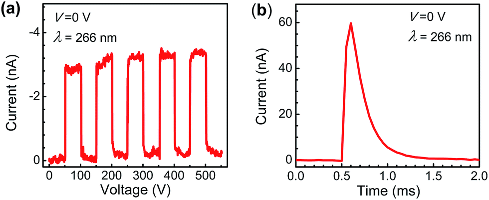 | ||
| Fig. 5 (a) Time-dependent photocurrent with periodic switching of 266 nm light illumination (0.01 mW cm−2). (b) Transient photoresponse using a Nd:YAG laser as an excitation source (266 nm, 10 ns). Note that all the measurements were carried out at zero bias at room temperature. | ||
Table 1 summarizes the key parameters of the typical vertical structure solar-blind UV photodetectors based on ZnMgO. The response speed of our Ag/ZnMgO/ZnO photodetector is much faster than that of other vertical structure ZnMgO solar-blind UV devices.18 Additionally, the peak responsivity of our device at 0 V is around 16 mA W−1, which is comparable with that of other self-powered devices.17–19
4. Conclusions
In summary, a self-powered solar-blind UV photodetector was demonstrated based on Ag/ZnMgO/ZnO structure on the a-sapphire substrate. ZnO layer was served as both the buffer layer to grow solar-blind w-ZnMgO and the bottom contact of the vertical structure device in this study. Due to electrons hopping the ZnMgO layer with the assistance of defects under bias, the device showed a nearly linear dark-current property. However, at 0 V, an obvious self-powered property can be observed because of the built-in electric fields at Ag/ZnMgO and ZnMgO/ZnO interfaces. The peak responsivity at 275 nm was around 16 mA W−1 with a −3 dB cutoff wavelength of 285 nm. The rise time and decay time were around 24 μs and 300 μs, respectively. Our findings prove a much easier and more feasible route to realize ZnMgO self-powered solar-blind photodetectors on foreign substrates, which have potential application for future solar-blind UV detection.Acknowledgements
This work was supported by the National Natural Science Foundation of China (No. 61475153), and the 100 Talents Program of the Chinese Academy of Sciences.References
- S. J. Pearton, F. Ren, Y.-L. Wang, B. H. Chu, K. H. Chen, C. Y. Chang, W. Lim, J. Lin and D. P. Norton, Prog. Mater. Sci., 2010, 55, 1 CrossRef.
- H. Chen, K. Liu, L. Hu, A. A. Al-Ghamdi and X. Fang, Mater. Today, 2015, 18, 493 CrossRef CAS.
- E. Cicek, R. McClintock, C. Y. Cho, B. Rahnema and M. Razeghi, Appl. Phys. Lett., 2013, 103, 191108 CrossRef.
- L. Zhang, S. Tang, C. Liu, B. Li, H. Wu, H. Wang, Z. Wu and H. Jiang, Appl. Phys. Lett., 2015, 107, 233501 CrossRef.
- D. Guo, Z. Wu, P. Li, Y. An, H. Liu, X. Guo, H. Yan, G. Wang, C. Sun, L. Li and W. Tang, Opt. Mater. Express, 2014, 4, 1067 CrossRef.
- X. Chen, K. W. Liu, Z. Z. Zhang, C. R. Wang, B. H. Li, H. F. Zhao, D. G. Zhao and D. Z. Shen, ACS Appl. Mater. Interfaces, 2016, 8, 4185 CAS.
- M. Liao, Y. Koide and J. Alvarez, Appl. Phys. Lett., 2005, 87, 022105 CrossRef.
- F. Mendoza, V. Makarov, B. R. Weiner and G. Morell, Appl. Phys. Lett., 2015, 107, 201605 CrossRef.
- M.-M. Fan, K.-W. Liu, X. Chen, X. Wang, Z.-Z. Zhang, B.-H. Li and D.-Z. Shen, ACS Appl. Mater. Interfaces, 2015, 7, 20600 CAS.
- Y. N. Hou, Z. X. Mei, Z. L. Liu, T. C. Zhang and X. L. Du, Appl. Phys. Lett., 2011, 98, 103506 CrossRef.
- X. L. Du, Z. X. Mei, Z. L. Liu, Y. Guo, T. C. Zhang, Y. N. Hou, Z. Zhang, Q. K. Xue and A. Y. Kuznetsov, Adv. Mater., 2009, 21, 4625 CrossRef CAS.
- F. J. Liu, Z. F. Hu, L. Zhu, Z. J. Li, H. Q. Huang, J. W. Zhao, X. Q. Zhang and Y. S. Wang, IEEE Trans. Electron Devices, 2012, 59, 1970 CrossRef CAS.
- Q. H. Zheng, F. Huang, J. Huang, Q. C. Hu, D. G. Chen and K. Ding, IEEE Electron Device Lett., 2012, 33, 1033 CrossRef CAS.
- Q. Zheng, F. Huang, K. Ding, J. Huang, D. Chen, Z. Zhan and Z. Lin, Appl. Phys. Lett., 2011, 98, 221112 CrossRef.
- T. Takagi, H. Tanaka, S. Fujita and S. Fujita, Jpn. J. Appl. Phys., 2003, 42, L401 CrossRef CAS.
- Z. P. Zhang, H. von Wenckstern and M. Grundmann, Appl. Phys. Lett., 2013, 103, 171111 CrossRef.
- H. L. Liang, Z. X. Mei, Q. H. Zhang, L. Gu, S. Liang, Y. N. Hou, D. Q. Ye, C. Z. Gu, R. C. Yu and X. L. Du, Appl. Phys. Lett., 2011, 98, 221902 CrossRef.
- Y. N. Hou, Z. X. Mei, H. L. Liang, D. Q. Ye, C. Z. Gu and X. L. Du, Appl. Phys. Lett., 2013, 102, 153510 CrossRef.
- H. Endo, M. Kikuchi, M. Ashioi, Y. Kashiwaba, K. Hane and Y. Kashiwaba, Appl. Phys. Express, 2008, 1, 051201 CrossRef.
- Ü. Özgür, Y. I. Alivov, C. Liu, A. Teke, M. A. Reshchikov, S. Dogǎn, V. Avrutin, S.-J. Cho and H. Morkoc, J. Appl. Phys., 2005, 98, 041301 CrossRef.
- X. Zhao, L. Chen, Y. He, J. Liu, W. Peng, Z. Huang, X. Qi, Z. Pan, W. Zhang, Z. Zhang and X. Ouyang, Appl. Phys. Lett., 2016, 108, 171103 CrossRef.
- K. W. Liu, M. Sakurai and M. Aono, Sensors, 2010, 10, 8604 CrossRef CAS PubMed.
- Y. Shen, X. Yan, Z. Bai, X. Zheng, Y. Sun, Y. Liu, P. Lin, X. Chen and Y. Zhang, RSC Adv., 2015, 5, 5976 RSC.
- Y. Lee, J. Kwon, E. Hwang, C.-H. Ra, W. J. Yoo, J.-H. Ahn, J. H. Park and J. H. Cho, Adv. Mater., 2015, 27, 41 CrossRef CAS PubMed.
- H. Zhou, J. Mei, P. Gui, P. Tao, Z. Song, H. Wang and G.-J. Fang, Mater. Sci. Semicond. Process., 2015, 38, 67 CrossRef CAS.
- J. Yu, X. Chen, Y. Wang, H. Zhou, M. Xue, Y. Xu, Z. Li, C. Ye, J. Zhang, P. A. v. Aken, P. D. Lund and H. Wang, J. Mater. Chem. C, 2016, 4, 7302 RSC.
- H. Zhou, P. Gui, Q. Yu, J. Mei, H. Wang and G. Fang, J. Mater. Chem. C, 2015, 3, 990 RSC.
- H. Zhou, Z. Song, P. Tao, H. Lei, P. Gui, J. Mei, H. Wang and G. Fang, RSC Adv., 2016, 6, 6205 RSC.
- Y. Kozuka, A. Tsukazaki and M. Kawasaki, Appl. Phys. Rev., 2014, 1, 011303 Search PubMed.
- Y.-Y. Chen, C.-H. Wang, G.-S. Chen, Y.-C. Li and C.-P. Liu, Nano Energy, 2015, 11, 533 CrossRef CAS.
- Z. Bai, X. Yan, X. Chen, Y. Cui, P. Lin, Y. Shen and Y. Zhang, RSC Adv., 2013, 3, 17682 RSC.
- Y. H. Ok, K. R. Lee, B. O. Jung, Y. H. Kwon and H. K. Cho, Thin Solid Films, 2014, 570, 282 CrossRef CAS.
- R. Karsthof, P. Räcke, H. von Wenckstern and M. Grundmann, Phys. Status Solidi A, 2016, 213(1), 30 CrossRef CAS.
- M. Grundmann, F. Klüpfel, R. Karsthof, P. Schlupp, F.-L. Schein, D. Splith, C. Yang, S. Bitter and H. von Wenckstern, J. Phys. D: Appl. Phys., 2016, 49, 213001 CrossRef.
- M. Guziewicz, R. Schifano, E. Przezdziecka, J. Z. Domagala, W. Jung, T. A. Krajewski and E. Guziewicz, Appl. Phys. Lett., 2015, 107, 101105 CrossRef.
- L. Su, Q. Zhang, T. Wu, M. Chen, Y. Su, Y. Zhu, R. Xiang, X. Gui and Z. Tang, Appl. Phys. Lett., 2014, 105, 072106 CrossRef.
- M. Ding, D. Zhao, B. Yao, Z. Li and X. Xu, RSC Adv., 2015, 5, 908 RSC.
- M. Nakano, T. Makino, A. Tsukazaki, K. Oeno, A. Ohtomo, T. Fukumura, H. Yuji, Y. Nishimoto, S. Akasaka, D. Takamizu, K. Nakahara, T. Tanabe, A. Kamisawa and M. Kawasaki, Appl. Phys. Express, 2008, 1, 121201 CrossRef.
- Z. Hu, Z. Li, L. Zhu, F. Liu, Y. Lv, X. Zhang and Y. Wang, Opt. Lett., 2012, 37, 3072 CrossRef CAS PubMed.
- À. Ohtomo, M. Kawasaki, T. Koida, K. Masubuchi, H. Koinuma, Y. Sakurai, Y. Yoshida, T. Yasuda and Y. Segawa, Appl. Phys. Lett., 1998, 72, 2466 CrossRef.
- M. M. Fan, K. W. Liu, Z. Z. Zhang, B. H. Li, X. Chen, D. X. Zhao, C. X. Shan and D. Z. Shen, Appl. Phys. Lett., 2014, 105, 011117 CrossRef.
- Y. Kozuka, J. Falson, Y. Segawa, T. Makino, A. Tsukazaki and M. Kawasaki, J. Appl. Phys., 2012, 112, 043515 CrossRef.
- M. Trunk, V. Venkatachalapathy, A. Galeckas and A. Yu. Kuznetsov, Appl. Phys. Lett., 2010, 97, 211901 CrossRef.
- Q. Shan, D. S. Meyaard, Q. Dai, J. Cho, E. F. Schubert, J. K. Son and C. Sone, Appl. Phys. Lett., 2011, 99, 253506 CrossRef.
- J. Dąbrowski, G. Lippert, L. Oberbeck, U. Schröder, I. Costina, G. Łupina, M. Ratzke, P. Zaumseil and H.-J. Müssig, J. Electrochem. Soc., 2008, 155, G97 CrossRef.
| This journal is © The Royal Society of Chemistry 2017 |