Micro organic light-emitting diodes fabricated through area-selective growth†
Juan
Zhu
ab,
Florian
Fontein
b,
Hong
Wang
b,
Qigang
Zhong
a,
Chenglong
Li
c,
Jianping
Li
a,
Bo
Wang
a,
Liangsheng
Liao
 a,
Yue
Wang
 c,
Lizhen
Huang
a,
Harald
Fuchs
b,
Wenchong
Wang
 *b and
Lifeng
Chi
 *a
*a
aInstitute of Functional Nano & Soft Materials (FUNSOM) and Jiangsu Key Laboratory for Carbon-based Functional Materials & Devices, Collaborative Innovation Center of Suzhou Nano Science and Technology, Soochow University, 199 Ren-ai Road, 215123 Suzhou, China. E-mail: chilf@suda.edu.cn
bPhysikalisches Institut and Center for Nanotechnology, Universität Münster, Wilhelm-Klemm-Straße 10, 48149 Münster, Germany. E-mail: wangw@uni-muenster.de
cState Key Laboratory for Supermolecular Structure and Materials College of Chemistry, Jilin University, 2699 Qianjin Street, 130012 Changchun, China
First published on 28th September 2017
Abstract
Developments in micro-displays have led to great interest in patterning OLEDs on the microscale. However, because organic molecules are fragile in adverse environments, patterning OLEDs on the microscale remains underdeveloped. In this work, the fabrication of Micro-OLEDs via the area-selective growth of hole-transporting material is reported. The active material is selectively deposited on pre-determined areas, and this technique is compatible with photolithography. High-resolution OLEDs with feature sizes as low as sub-micrometer and green-, orange-red- and deep-blue-emitting devices are demonstrated. This technique provides a promising method for the fabrication of high-resolution OLED devices over large areas.
Introduction
Inorganic micro light-emitting diodes (Micro-LEDs) consist of microscopic light-emitting diode arrays with typical diameters of 4–20 μm, forming the individual pixel element.1 Over the past two decades, Micro-LEDs have drawn increasing attention, owing to their extensive applicability to devices such as displays, light communications, and their advantages of high light output efficiencies, low cost, fast response time and low power consumption in comparison to their traditional counterparts.2,3 Since 2000, inorganic Micro-LEDs have been successfully developed through lithography, dry/wet etching and device transfer processes.3–6 However, the patterning of Micro-OLEDs, as organic counterparts, is still underdeveloped, owing to the degradation or complete failure of the devices after exposure to water vapor, oxygen, solvents or developers used in the removal or patterning of photoresists.7–12 Attempts to fabricate Micro-OLEDs through unconventional methods, such as shadow masks, stamping and beam writing, have the drawbacks of low resolution, nonuniformity over large areas and poor yield.13–18 Recently, orthogonal photolithography has been demonstrated as an alternative method to fabricate Micro-OLEDs with micrometer resolution by using specific photoresists and orthogonal solvents.19–23Alternatively, area-selective growth, which allows material to be selectively grown on pre-determined patterns, has been proposed to pattern organic semiconductors.24 The pre-patterns, which can be produced by photolithography, act as nucleation sites for the diffusion of organic semiconductor molecules over the surface under vacuum. The area-selective growth strategy has successfully been applied to different kinds of molecules to achieve functional molecular architectures and improve device performance.25–27
In this work, we report the fabrication of Micro-OLEDs by using the area-selective growth method. The active material was controlled to grow on pre-defined areas, and further processed to create OLED devices. A patterned thin layer of Cr and Au on indium tin oxide (ITO) glass acted as the nucleation site for organic semiconductor molecules, and the ITO glass covered the layered metal structures had a transmittance of 70–75%. The emitting area of the Micro-OLEDs was defined by the pre-structures, where high-resolution structures with feature sizes as low as hundreds of nanometers were achieved. Green-, orange-red- and blue-emitting OLEDs made from the same hole-transporting material, NPB (N,N′-di(1-naphthyl)-N,N′-diphenyl-(1,1′-biphenyl)-4,4′-diamine), were successfully fabricated through this technique. The green-emitting OLED devices (ITO/(Cr + Au)/NPB/tris-(8-hydroxyquinoline)aluminum (Alq3)/Al) showed similar luminescence intensity and threshold voltage to those of the traditional device structure (ITO/NPB/Alq3/Al). This technique is fully compatible with photolithography and provides an alternative method to process OLED devices with high resolution and yield over macroscopic areas.
Experimental
Materials
NPB (sublimed grade, 99%), Alq3 (sublimed grade, 99.995%), DCM (dye content 98%) and TPBI were purchased from Sigma-Aldrich. PPI-PPITPA was synthesized according to previously described technique.28 The full name and structures of chemicals were shown in Fig. S1 (ESI†). ITO-coated polished glass substrates (resistance ≤80 Ohms sq−1) were purchased from Präzisions Glas & Optik GmbH. The metal materials used for evaporation, including the Cr rod, Au wire and Al wire, were purchased from MaTecK. All the materials were used without further purification.Pre-pattern fabrication
The ITO-coated glass substrates were ultrasonically cleaned in acetone, ethanol and de-ionized water, blown dry with high-purity N2 gas and used for e-beam lithography. A PMMA layer with a thickness of 300 nm was first spin-coated on the ITO-coated glass substrate. An Elphy 100 system attached to a LEO 1530 VP Gemini electron microscope was used for e-beam lithography. After e-beam lithography, the substrates with exposed PMMA were developed in photographic developer and loaded into a vacuum chamber to coat the metal layers via thermal deposition, first with a Cr adhesion layer (2 nm) and then with an Au layer (3 nm). The samples were submerged in acetone for 60 minutes of ultrasonic cleaning, subsequently cleaned in acetone, ethanol and de-ionized water, and stored in de-ionized water before use.Film deposition of organic materials
A homemade vacuum system with three evaporate-cells was used to deposit the organic materials; NPB, Alq3, DCM, PPI-PPITPA and TPBI were used in the experiment. Before being loaded into the vacuum system, the samples were treated with O2 plasma at 1 mbar and 300 watts for 5 minutes. The organic molecules were sublimed from a quartz crucible and transported to the substrate at a constant deposition rate. As shown in Fig. S5 (ESI†), different emission systems based on NPB as the hole-transporting layer were used to obtain green, orange-red and deep-blue emission. NPB was first grown on the substrates at a deposition rate of 1 nm min−1, and the substrates were kept at 220 °C. After NPB deposition, the samples were cooled to room temperature in vacuum for subsequent layer deposition. For the green-emitting OLEDs, Alq3 was deposited as the electron-transporting/emitting layer. For the orange-red-emitting OLEDs, a layer of Alq3:DCM (2%) was co-evaporated as the emitting layer, and Alq3 was subsequently grown as the electron-transporting layer. For the blue-emission system, PPI-PPITPA was evaporated on the sample as the emitter, and then, TPBI was grown as the electron-transporting and hole-blocking layer.Cathode deposition
The as-grown samples were removed from the vacuum chamber and loaded into another vacuum chamber (E306 Edwards) to grow the Al cathode. A 120 nm layer of Al was deposited on top of the device at a rate of 0.5 nm s−1 by heating tungsten wire under a high vacuum of 10 × 10−6 mbar.Atomic force microscopy
AFM measurements were performed with a commercial instrument (Digital Instruments, Nanoscope IIIa, Dimension 300) in tapping mode (Si cantilevers with spring constants 250–350 kHz).Microscopy
An Olympus microscope BX-FLA (made in Hamburg, Germany) equipped with a CCD camera and an objective was used to obtain the optical microscopy and electroluminescence images.EL spectra, intensity and mapping
The spectra were collected using a Princeton Instruments Model 320PI (grating 300 lp mm−1) spectrograph with a liquid nitrogen cooled camera (Spec-10:400B). During the measurement process, the electroluminescence intensity increased with voltage, the optical signals were detected with an avalanche photodiode (EG&G SPCM-200PQ), and the output pulses were converted to voltage by integration over a time of milliseconds with a homemade counter/integrator and measured by a digital storage oscilloscope (Tektronix TDS 2002B) together with the applied voltage.The mapping images were obtained by using a homemade instrument consisting of an inverted microscope (Nikon Diaphot 300) and a closed-loop piezo scanner (Physik Instrumente P-517.3CL) controlled by a Nanotec SPM controller. The optical signals were detected by the same avalanche photodiode as used for the EL intensity measurement. The output pulses were converted to voltage with the same counter/integrator and measured by the SPM controller.
Transmittance measurements
The transmittance spectra were measured by using a Hitachi U-3000 spectrophotometer.Results and discussion
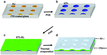
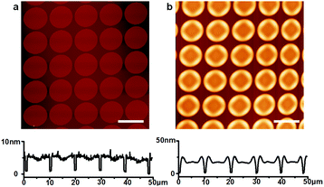
The fabrication process for the Micro-OLED devices is illustrated in Fig. 1. The pre-patterns shown in Fig. 1a were generated by standard e-beam lithography on ITO glass spin-coated with a poly(methyl methacrylate) (PMMA) layer. After PMMA was exposed to the electron beam and developed, a Cr adhesion layer and a thin Au layer were sequentially deposited via thermal deposition. After lift-off and a cleaning process in organic solvents, the pre-patterned substrates were loaded into a vacuum chamber for deposition of the hole-transporting layer. Fig. 1b schematically illustrates the area-selective growth of a selected material on the pre-patterned substrate via vapor deposition while the substrates were heated to a certain temperature. Activated by the temperature of the substrate, the deposition molecules diffused more easily on the surface and nucleated on the Au area, owing to the larger binding energy of the molecules with Au compared with that of ITO. The diffusion length of the molecules can be controlled by the growth parameters, e.g., substrate temperature and grow rate. When the periodicity of the Au dot array is shorter than the diffusion length of the molecules, all molecules can grow on the Au areas. When the periodicity is larger than the diffusion length, some of the molecules will aggregate and nucleate on the ITO glass.24 The side view in Fig. 1b depicts the typical morphology of the hole-transporting layer selectively grown on the pre-patterns. After the hole-transporting layer was grown on the pre-defined areas, an electron-transporting/emitting layer was successively deposited on the samples, as shown in Fig. 1c. Finally, the Al cathode layer was successively deposited as the top electrode of the OLED device via thermal evaporation, as demonstrated in Fig. 1d.Fig. 2a shows the AFM height image and profile of the pre-patterns, in which the average height is approximately 5 nm and consists of 2 nm Cr and 3 nm Au. The thickness of the metal layer was optimized for both homogeneous nucleation sites and transmittance, as discussed in the following transmission spectra. The pre-patterns consisted of an array of dots with diameters of 9 μm and spacings of 1.5 μm. NPB was chosen as the hole-transporting material in the OLEDs, because sublimed NPB can be manufactured readily and is abundantly available.29 In the experiments, the substrate temperature was optimized at 220 °C, so that the diffusion length of the molecules was larger than the pattern spacing, and the molecules could be fully controlled to grow only on the Au patterns. Fig. 2b shows the AFM height image and profile of 8 nm NPB (controlled by a microbalance adjacent to the samples) deposited on the sample. The organic molecules were clearly seen to remain only on the Au dots, and more molecules aggregated around the edge of the metal patterns, owing to the collection of molecules deposited on ITO. The average height of the NPB films at the center of the Au dots was approximately 15 nm, and that at the edges was approximately 20 nm. The morphology of NPB depended on the diameter of the Au dots. As the diameter of Au decreased to below 5 μm, the morphology of NPB became dome-like, thus indicating the shift of molecules to the center of the dots. The growth of NPB on the Au pattern with a diameter of 0.5 μm shown in Fig. S2 (ESI†) was taken as an example. The fully area-selective growth is further confirmed by the calculated results in Table S1 (ESI†). It is shown that the amount of NPB on top of Au calculated by AFM software has a negligible error with the total amount of NPB deposited on the whole substrate in both cases.
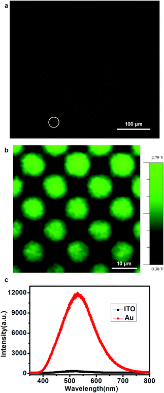
To fabricate the OLED devices, we deposited 70 nm Alq3, as both the electron-transporting and emitting layer, on the patterned NPB layer after the samples were cooled to room temperature, and then deposited 120 nm Al as the cathode. The electroluminescence of the devices under a drive voltage 18 V was first characterized by optical microscopy between the bottom ITO anode and the Al cathode. The luminescence microscopy image of a device is shown in Fig. 3a. A bright luminescence region was observed at a pitch of 10.5 μm (center-to-center), which coincided with the dimensions of the pre-patterned Au templates. A homemade instrument consisting of an inverted microscope and a closed-loop piezo scanner manipulated by an SPM controller was further used to scan the luminescence patterns under the same voltage. The optical signals were detected with a photodiode, and the output pulses were converted to voltage with a counter/integrator and measured by the SPM controller. The luminescence mapping is shown in Fig. 3b. In the image, the color contrast represents the luminescence intensity. During the 20-minute scanning process of the mapping image, almost no change in the mapping image was observed. Fig. 3c presents the luminescence spectra on Au (red line) and on ITO (black line). Because the limited mapping step size of 2.5 micrometers was larger than the pitch size of 1.5 micrometers, luminescence signals on ITO glass were taken in the vicinity of the patterning area highlighted by the white circle in the lower-left region of Fig. 3a. The luminescence intensity on the Au dots (maximum value is 12![[thin space (1/6-em)]](https://www.rsc.org/images/entities/char_2009.gif) 000) was much higher than that nearby on ITO glass (maximum value is 300). We believe that the difference in the luminescence intensity on the Au dots and ITO glass would be even greater, owing to the nonnegligible background light produced by the thick layer of NPB particles on the ITO glass substrate. Thus, high-contrast illuminated images can be fabricated through this technique.
000) was much higher than that nearby on ITO glass (maximum value is 300). We believe that the difference in the luminescence intensity on the Au dots and ITO glass would be even greater, owing to the nonnegligible background light produced by the thick layer of NPB particles on the ITO glass substrate. Thus, high-contrast illuminated images can be fabricated through this technique.
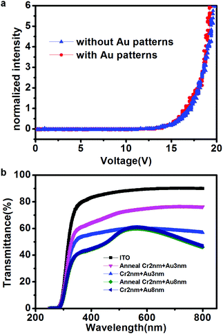
Fig. 4a shows the normalized electroluminescence intensity versus the device voltage. The devices fabricated with our technique (red line) showed typical OLED behavior and similar luminance characteristics to those of devices fabricated with the classic structure (ITO/NPB (20 nm)/Alq3 (70 nm)/Al (120 nm)). The relatively higher drive voltage may be attributed to the high barrier between the Fermi level of the cathode and the HOMO level of the organic layer.30–32 The drive voltage can be lowered by inserting a LiF layer before deposition of the Al cathode layer.31 Although the substrate with the thin metal layer used in our technique has a comparatively weaker transmittance, a similar luminescence intensity was realized at the same applied voltage. An energy level difference between the ITO anode and NPB (0.7 eV) is known to provide a high barrier for hole injection in classic devices. It is speculated that the presence of Au (work function: 5.1 eV) decreases this barrier, thus facilitating hole injection and improving the device performance.33 However, the similar turn-on voltage on these two devices shown in Fig. 4a is possibly caused by the strong interfacial dipole formed at the metal/organic interface, the chemical residual in the e-beam lithography process or the alloy formation between interfaces, which will be further investigated in the future experiments.34–36 The transmittance of the transparent electrodes, so that the luminescence can pass through, is one of the most important parameters in evaluating the properties of OLED devices. Fig. 4b shows the transmittance spectra as a function of wavelength in the range of 250–800 nm for the samples tested in the experiments. The ITO-coated glass (black line) possessed the greatest transmittance of up to 90%. The blue and dark-blue lines represented the transmittance spectra of 3 nm and 8 nm Au, respectively, on ITO glass substrates coated with a 2 nm adhesion Cr layer. The transmittance clearly decreased as the thickness of Cr and Au coated on the ITO glass increased. The transmittance was further characterized after annealing at 220 °C to simulate the NPB deposition process. The transmittance of the sample deposited with 2 nm Cr and 8 nm Au after annealing, indicated by the green line, overlapped with the previous dark-blue line. Therefore, no change occurred in the transmittance spectrum of the film after annealing, a result consistent with the continuous thick Au film possessing a strong absorption at 450 nm.37 In comparison, the transmittance of the 2 nm Cr and 3 nm Au film on ITO glass at 560 nm increased from 60% (blue line) to 75% (pink line) after annealing. Only a slight change occurred in the transmittance of the 2 nm Cr film on ITO glass at 560 nm after annealing, increasing from 80% (black line) to 85% (red line), as shown in Fig. S3 (ESI†). The transmittance increase after annealing indicated lower surface roughness and better homogeneity, which was further verified by the AFM height images of the sample with 2 nm Cr and 3 nm Au after annealing, shown in Fig. S4, in which the sample had a higher surface roughness before annealing (before: 0.85; after: 0.73). The formation of an alloy between Cr, ITO and/or Au when the sample is annealed at high temperature has been predicted to cause the improved homogeneity and transmittance.38 Although the substrate with a thin Cr layer has a higher transmittance, Au has a higher work function, which can thus improve hole injection in the OLED devices. Therefore, the optimal film was composed of 2 nm Cr, for better adhesion, and 3 nm Au.
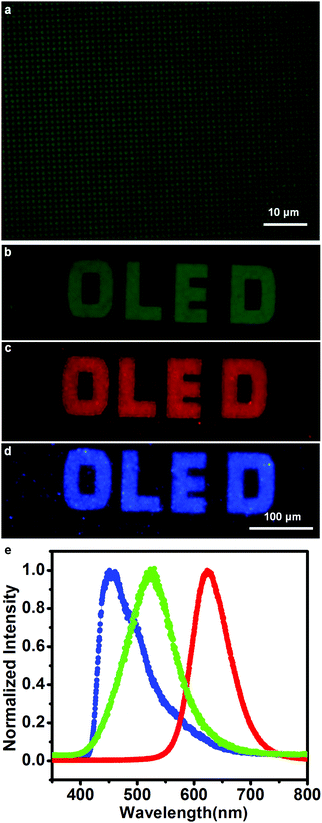
This technique was further extended to create Micro-OLEDs with arbitrary shapes. High-resolution emitting dot patterns with a diameter of 0.5 μm are shown in Fig. 5a. AFM height images of the Au dots and after NPB growth are exhibited in Fig. S2 (ESI†). The morphology of the organic materials on the Au dots was consistent with that shown in the schematic diagram (Fig. 1b). Luminescence patterns with large sizes and spacings were also fabricated with this technique for example, the letters ‘OLED’ with a 20 μm line width were fabricated and are exhibited in Fig. 5b. The feasibility of this technique was further characterized using an orange-red-emission system based on ITO/NPB (20 nm)/Alq3:DCM (35 nm, 1%)/Alq3 (35 nm)/Al, as well as a deep-blue-emission system based on ITO/NPB (20 nm)/PPI-PPITPA (30 nm)/TPBI (50 nm)/Al (120 nm). The molecular and device structures can be found in Fig. S1 and S5 (ESI†). A small amount of DCM (4-(dicyanomethylene)-2-methyl-6-(4-dimethylaminostyryl)-4H-pyran) was physically doped in the emitting layer, which changes the color of the emitted light from green to orange-red.39 PPI-PPITPA is an excellent deep-blue luminescent material, which has an ideal donor-accept molecular structure and packing in the solid state and small singlet–triplet splitting.28 Orange-red and deep-blue emission patterns are shown in Fig. 5c and d, respectively. The blue, orange-red and green emissions were further characterized by spectrophotometer. Fig. 5e shows the corresponding luminescence spectra of the three different color devices, where the signal peaks are located at the typical locations for deep-blue, green and orange-red (460 nm, 528 nm and 625 nm, respectively). This technique was thus demonstrated to be an easily used method for patterning OLEDs with different emission colors via area-selective growth.
Conclusions
The fabrication of Micro-OLEDs with arbitrary shape and size was presented here. High-resolution emission patterning with feature sizes as low as hundreds of nanometers were realized via selective growth of the hole-transporting material (NPB) on a pre-defined area. Light-emitting devices based on NPB showing green, orange-red and deep-blue emission were successfully fabricated. The excellent device performance was characterized through various techniques, including fluorescence mapping, luminescence spectroscopy and transmission spectroscopy. The technique presented here is compatible with other patterning techniques, such as photolithography and soft lithography, and provides an alternative method for the fabrication of high-resolution OLED devices over large areas.40Author contributions
L. C., W. W. and F. H. initiated the project. L. C., W. W. and J. Z. designed the experiments. J. Z. performed device fabrication and measurements. F. F. obtained the fluorescence spectra and mapping. H. W. performed the experiments given in Fig. S2 (ESI†). Q. Z. drew the schematic diagram. C. L. and Y. W synthesized the molecules. J. L. assisted the measurements of luminescent spectra. B. W. and L. L. discussed the experiment. L. C., W. W. and J. Z. interpreted the data and wrote the manuscript. All authors read and commented on the manuscript.Conflicts of interest
There are no conflicts of interest to declare.Acknowledgements
This work was supported by the German-Chinese Transregional Collaborative Research Centre TRR 61 (B1) by DFG and the National Natural Science Foundation of China (No. 21661132006 and 21527805). J. Zhu is grateful to the China Scholarship Council for their financial support. We also would like to thank Mr Zhiqiang Liang, Mr Jing Wei and Miss Jianmei Chen for their assistance in fabricating the electrodes and AFM characterization.Notes and references
- H. W. Choi, C. Liu, E. Gu, G. McConnell, J. M. Girkin, I. M. Watson and M. D. Dawson, Appl. Phys. Lett., 2004, 84, 2253–2255 CrossRef CAS.
- S. X. Jin, J. Li, J. Z. Li, J. Y. Lin and H. X. Jiang, Appl. Phys. Lett., 2000, 76, 631–633 CrossRef CAS.
- B. Thibeault and S. DenBaars, US Pat., 6410942, 2002 Search PubMed.
- H. W. Choi, C. W. Jeon, M. D. Dawson, P. R. Edwards and R. W. Martin, IEEE Photonics Technol. Lett., 2003, 15, 510–512 CrossRef.
- H. W. Choi, C. W. Jeon and M. D. Dawson, J. Cryst. Growth, 2004, 268, 527–530 CrossRef CAS.
- S.-K. Kang, US Pat., 7906787, 2011 Search PubMed.
- N. Thejo Kalyani and S. J. Dhoble, Renewable Sustainable Energy Rev., 2012, 16, 2696–2723 CrossRef CAS.
- B. Geffroy, P. Le Roy and C. Prat, Polym. Int., 2006, 55, 572–582 CrossRef CAS.
- S. R. Forrest, Nature, 2004, 428, 911–918 CrossRef CAS PubMed.
- E. Menard, M. A. Meitl, Y. G. Sun, J. U. Park, D. J. L. Shir, Y. S. Nam, S. Jeon and J. A. Rogers, Chem. Rev., 2007, 107, 1117–1160 CrossRef CAS PubMed.
- C. W. Tang and S. A. Vanslyke, Appl. Phys. Lett., 1987, 51, 913–915 CrossRef CAS.
- L. Duan, L. Hou, T.-W. Lee, J. Qiao, D. Zhang, G. Dong, L. Wang and Y. Qiu, J. Mater. Chem., 2010, 20, 6392–6407 RSC.
- M. Shtein, P. Peumans, J. B. Benziger and S. R. Forrest, J. Appl. Phys., 2003, 93, 4005–4016 CrossRef CAS.
- J. Choi, D. Kim, P. J. Yoo and H. H. Lee, Adv. Mater., 2005, 17, 166–171 CrossRef CAS.
- D. G. Lidzey, M. Voigt, C. Giebeler, A. Buckley, J. Wright, K. Böhlen, J. Fieret and R. Allott, Org. Electron., 2005, 6, 221–228 CrossRef CAS.
- K. M. Knesting, P. J. Hotchkiss, B. A. MacLeod, S. R. Marder and D. S. Ginger, Adv. Mater., 2012, 24, 642–646 CrossRef CAS PubMed.
- C. Zhong, C. Duan, F. Huang, H. Wu and Y. Cao, Chem. Mater., 2011, 23, 326–340 CrossRef CAS.
- H. Zheng, Y. Zheng, N. Liu, N. Ai, Q. Wang, S. Wu, J. Zhou, D. Hu, S. Yu, S. Han, W. Xu, C. Luo, Y. Meng, Z. Jiang, Y. Chen, D. Li, F. Huang, J. Wang, J. Peng and Y. Cao, Nat. Commun., 2013, 4, 1971 Search PubMed.
- A. A. Zakhidov, J.-K. Lee, H. H. Fong, J. A. DeFranco, M. Chatzichristidi, P. G. Taylor, C. K. Ober and G. G. Malliaras, Adv. Mater., 2008, 20, 3481–3484 CrossRef CAS.
- H. H. Fong, J. K. Lee, Y. F. Lim, A. A. Zakhidov, W. W. Wong, A. B. Holmes, C. K. Ober and G. G. Malliaras, Adv. Mater., 2011, 23, 735–739 CrossRef CAS PubMed.
- P. C. Taylor, J. K. Lee, A. A. Zakhidov, M. Chatzichristidi, H. H. Fong, J. A. DeFranco, G. C. Malliaras and C. K. Ober, Adv. Mater., 2009, 21, 2314–2317 CrossRef CAS.
- S. Krotkus, F. Ventsch, D. Kasemann, A. A. Zakhidov, S. Hofmann, K. Leo and M. C. Gather, Adv. Opt. Mater., 2014, 2, 1043–1048 CrossRef CAS.
- S. Krotkus, D. Kasemann, S. Lenk, K. Leo and S. Reineke, Light: Sci. Appl., 2016, 5, e16121 CrossRef CAS.
- W. Wang, D. Zhong, J. Zhu, F. Kalischewski, R. Dou, K. Wedeking, Y. Wang, A. Heuer, H. Fuchs and G. Erker, Phys. Rev. Lett., 2007, 98, 225504 CrossRef CAS PubMed.
- W. Wang, C. Du, D. Zhong, M. Hirtz, Y. Wang, N. Lu, L. Wu, D. Ebeling, L. Li, H. Fuchs and L. Chi, Adv. Mater., 2009, 21, 4721–4725 CAS.
- W. Wang and L. Chi, Acc. Chem. Res., 2012, 45, 1646–1656 CrossRef CAS PubMed.
- W. Wang, C. Du, L. Li, H. Wang, C. Wang, Y. Wang, H. Fuchs and L. Chi, Adv. Mater., 2013, 25, 2018–2023 CrossRef CAS PubMed.
- C. L. Li, S. P. Wang, W. P. Chen, J. B. Wei, G. C. Yang, K. Q. Ye, Y. Liu and Y. Wang, Chem. Commun., 2015, 51, 10632–10635 RSC.
- L. Hung and C. Chen, Mater. Sci. Eng., R, 2002, 39, 143–222 CrossRef.
- G. G. Malliaras, J. R. Salem, P. J. Brock and J. C. Scott, Phys. Rev. B: Condens. Matter Mater. Phys., 1999, 59, 10371 CrossRef CAS.
- M. G. Mason, C. W. Tang, L.-S. Hung, P. Raychaudhuri, J. Madathil, D. J. Giesen, L. Yan, Q. T. Le, Y. Gao, S.-T. Lee, L. S. Liao, L. F. Cheng, W. R. Salaneck, D. A. dos Santos and J. L. Brédas, J. Appl. Phys., 2001, 89, 2756–2765 CrossRef CAS.
- Y. H. Lee, W. J. Kim, T. Y. Kim, J. Jung, J. Y. Lee, H. D. Park, T. W. Kim and J. W. Hong, Curr. Appl. Phys., 2007, 7, 409–412 CrossRef.
- I.-M. Chan, T.-Y. Hsu and F. C. Hong, Appl. Phys. Lett., 2002, 81, 1899–1901 CrossRef CAS.
- Z. Wang, M. Helander, J. Qiu, D. Puzzo, M. Greiner, Z. Hudson, S. Wang, Z. Liu and Z. Lu, Nat. Photonics, 2011, 5, 753 CrossRef CAS.
- H. Ishii, K. Sugiyama, E. Ito and K. Seki, Adv. Mater., 1999, 11, 605–625 CrossRef CAS.
- T. L. Belenkova, D. Rimmerman, E. Mentovich, H. Gilon, N. Hendler, S. Richter and G. Markovich, J. Mater. Chem., 2012, 22, 24042–24047 RSC.
- Y. S. Kim, J. H. Park, D. H. Choi, H. S. Jang, J. H. Lee, H. J. Park, J. I. Choi, D. H. Ju, J. Y. Lee and D. Kim, Appl. Surf. Sci., 2007, 254, 1524–1527 CrossRef CAS.
- G.-S. Heo, J.-W. Park, S.-E. Choi, M. H.-C. Jin and D.-C. Shin, Thin Solid Films, 2009, 518, 1160–1163 CrossRef CAS.
- C. T. Chen, Chem. Mater., 2004, 16, 4389–4400 CrossRef CAS.
- W. Wang, C. Du, C. Wang, M. Hirtz, L. Li, J. Hao, Q. Wu, R. Lu, N. Lu, Y. Wang, H. Fuchs and L. Chi, Small, 2011, 7, 1403–1406 CrossRef CAS PubMed.
Footnote |
| † Electronic supplementary information (ESI) available. See DOI: 10.1039/c7qm00383h |
| This journal is © the Partner Organisations 2017 |

