
Organic–inorganic hybrid photoresists containing hexafluoroantimonate: design, synthesis and high resolution EUV lithography studies†
Pulikanti
Guruprasad Reddy
 a,
Pawan
Kumar
b,
Subrata
Ghosh
a,
Chullikkattil P.
Pradeep
*a,
Satinder K.
Sharma
*b and
Kenneth E.
Gonsalves
*a
a,
Pawan
Kumar
b,
Subrata
Ghosh
a,
Chullikkattil P.
Pradeep
*a,
Satinder K.
Sharma
*b and
Kenneth E.
Gonsalves
*a
aSchool of Basic Sciences, Indian Institute of Technology Mandi, Kamand-175005, Himachal Pradesh, India. E-mail: pradeep@iitmandi.ac.in; Kenneth@iitmandi.ac.in; Fax: +91 1905 267 009; Tel: +91 1905 267 045
bSchool of Computing and Electrical Engineering, Indian Institute of Technology Mandi, Kamand-175005, Himachal Pradesh, India. E-mail: satinder@iitmandi.ac.in
First published on 12th September 2017
Abstract
Although many organic polymer based photoresists are useful for patterning high resolution sub-20 nm technology nodes, many such resists suffer from poor sensitivity. One of the methods to address the problem of low sensitivity is to incorporate inorganic components into the organic polymer resist formulations. The present work demonstrates the incorporation of an inorganic counter-ion moiety, hexafluoroantimonate, into an organic polymer photoresist, poly(4-(methacryloyloxy))phenyldimethylsulfoniumtriflate (poly-MAPDST), to improve its sensitivity. This approach resulted in two novel radiation sensitive hybrid non-chemically amplified resists (n-CARs), 1.5%-&2.15%-MAPDSA–MAPDST, having different percentages (1.5%&2.15% respectively) of MAPDSA incorporated into a poly-MAPDST backbone (where MAPDSA = (4-(methacryloyloxy)phenyl)dimethylsulfonium hexaflouroantimonate). These hybrid resists are sensitive towards extreme ultraviolet (EUV, λ = ∼13.5 nm) radiation and successfully patterned high resolution 20 nm lines as well as various complex nano-features including waves, boats, line-elbows, dots and circular patterns. The sensitivity exhibited by the 1.5%-&2.15%-MAPDSA–MAPDST resists was calculated to be 58.1 mJ cm−2 and 24.5 mJ cm−2, respectively, from normalized remaining thickness (NRT) curve anaylsis, which reveals improved sensitivity as compared to the poly-MAPDST resist.
Introduction
The rapid progress achieved in the semiconductor industry over the past few decades in terms of increased circuit element density and size miniaturization in accordance with Moore's law1 has put enormous pressure on photoresist technology to meet targeted resolutions.2–4 Among the various high resolution lithographic techniques such as 193 nm immersion, extreme ultraviolet lithography (EUVL), electron beam lithography (EBL), helium-ion beam (HIM) and X-ray lithography etc., EUVL (λ = 13.5 nm) shows many advantages over its counterparts to pattern high resolution features at sub-10 nm resolution.5–10 Although EUVL is fast approaching the commercialization phase as one of the most promising next generation lithography (NGL) tools, many challenges associated with this technology are yet to be fully addressed, including the scarcities of (a) a suitable EUV power source, (b) defect-free masks, (c) highly reflective optics and (d) suitable resist technologies.11,12 A potential EUV photoresist is expected to possess very high optical absorption, acceptable degassing properties, high etch resistance, good adhesion properties and defect-free pattern formation with an environment friendly developer.3,9,10 Therefore, in order to facilitate the commercialization of EUV technology for next generation semiconductor industry applications, simultaneous monitoring of the resist sensitivity, resolution, etch resistance and line edge roughness (LER) is essential.13 To date, chemically amplified resists (CARs) have been the work horses for the integrated circuit (IC) manufacturing industry.14–17 However, undesirable traits like post exposure instability, acid diffusion, lower sensitivity, higher line-edge & line-width roughness (LER & LWR) often exhibited by CARs limit the ultimate half pitch resolution attainable; particularly for sub-20 nm patterning applications.18–20 Therefore, in order to address some of the inherent problems associated with CARs and to meet the targets set by the international roadmap for semiconductors (ITRS)-2015, researchers have focused their attention on the development of non-chemically amplified resists (n-CARs) in recent years.21,22 Accordingly, a wide range of n-CARs with acceptable LER/LWR properties for patterning a 20 nm technology node or beyond have been developed by various groups over the past few years.3,4,23–33It has been noted that the sensitivity and etch resistance of organic n-CARs may be enhanced considerably by incorporating inorganic components into the resist formulation.3,4,34 We recently demonstrated the potential of a new class of negative tone n-CARs, poly-MAPDST [poly(4-(methacryloyloxy))phenyldimethylsulfoniumtriflate], for patterning 20 nm line features as well as complex nano-features under EUVL conditions.35,36 The present work demonstrates our approach to improve the lithographic performances of poly-MAPDST by incorporating hexafluoroantimonate (SbF6−) as an inorganic counter-ion moiety into the polymer network. Using this approach, we have developed two new radiation sensitive negative tone hybrid n-CARs, 1.5%-&2.15%-MAPDSA–MAPDST (1.5% and 2.15% resists hereafter), bearing 1.5% and 2.15%, respectively, of MAPDSA units in a poly-MAPDST network (where MAPDSA = (4-(methacryloyloxy)phenyl)dimethylsulfoniumhexaflouroantimonate, see, Scheme 1).
 | ||
| Scheme 1 Synthetic route of 1.5%-&2.15-MAPDSA–MAPDST copolymer resists. | ||
Experimental section
Materials and methods
Dichloromethane (HPLC grade) was purchased from Merck, India, and dried by using calcium hydride before use. Tetramethylammonium hydroxide (TMAH) was purchased from Sigma Aldrich, India. Fourier transform infrared spectroscopy (FT-IR) spectra were recorded on a Perkin Elmer Spectrum 2 spectrophotometer using KBr pellets. 1H, 13C and 19F nuclear magnetic resonance (NMR) spectra were recorded on a Jeol JNM ECX 500 MHz spectrometer in DMSO-d6 solvent. Molecular weight (Mw) and polydispersity index (PDI) of 1.5% and 2.15% resists were determined by performing gel permeation chromatography (GPC) analyses using PL gel mixed-B column on a 1260 Infinity Series instrument from Agilent. The Micro Exposure Tool (MET) with an advanced light source (ALS) at Lawrence Berkeley National Laboratory (LBNL) was used as the lithography tool for EUVL studies. The mask used for the nano-lithographic patterning was IMO228775. Film thicknesses were measured by using a NanoMap-D stylus profilometer. Field Emission Scanning Electron Microscopy (FE-SEM-Carl Zeiss, Ultra Plus) and Atomic Force Microscopy (AFM – Dimension Icon from Bruker) were utilized for investigating the critical dimensions (CD) of the line and other complex patterns (nano-waves, nano-boats, nano-rings, nano-dots, and line/star-elbow connections etc.) obtained from the 1.5% and 2.15% resists.Synthesis of (4-(methacryloyloxy)phenyl)dimethylsulfoniumtetrafluoroantimonate (MAPDSA)
A solution of iodomethane (0.53 mL, 8.64 mmol) in acetonitrile (2 mL) was added drop-wise to a mixture of 4-(methylthio)phenylmethacrylate35 (1.5 g, 7.20 mmol) and silver hexafluoroantimonate (2.47 g, 7.20 mmol) in acetonitrile (20 mL) at 0 °C under nitrogen in the dark. After 12 h of stirring, the formed silver iodide precipitate in the reaction mixture was filtered out and washed with 20 mL of acetonitrile. The collected filtrates were concentrated in a rotary evaporator and the resultant crude product was purified by washing several times with dichloromethane to give the pure white solid of MAPDSA. Yield: 0.920 g (75%). IR absorption: νmax/cm−1 3038–2946 (CH), 1731 (C![[double bond, length as m-dash]](https://www.rsc.org/images/entities/char_e001.gif) O), 1635–1584–1552 (CC), 1493, 1427, 1289, 1212, 1172, 1122, 1042 (C–O), 998, 957, 876 and 810. 1H NMR (500 MHz; DMSO-d6): δH = 2.01 (3H, s, CH3), 3.27 (6H, s, SCH3), 5.96 (1H, s, CCH), 6.32 (1H, s, CCH), 7.58 (2H, dt, J = 8.9 Hz, ArH), 8.14 (2H, dt, J = 8.9 Hz, ArH); 13C NMR (125 MHz; DMSO-d6): δC = 164.81 (CO), 154.49, 134.84, 131.73, 128.73, 124.12, 123.78 (aromatic), 28.40 (SCH3), 17.98 (CH3); 19F NMR (376 MHz; DMSO-d6): δF = −109.02 to −129.78 (6F, m, SbF6−).
O), 1635–1584–1552 (CC), 1493, 1427, 1289, 1212, 1172, 1122, 1042 (C–O), 998, 957, 876 and 810. 1H NMR (500 MHz; DMSO-d6): δH = 2.01 (3H, s, CH3), 3.27 (6H, s, SCH3), 5.96 (1H, s, CCH), 6.32 (1H, s, CCH), 7.58 (2H, dt, J = 8.9 Hz, ArH), 8.14 (2H, dt, J = 8.9 Hz, ArH); 13C NMR (125 MHz; DMSO-d6): δC = 164.81 (CO), 154.49, 134.84, 131.73, 128.73, 124.12, 123.78 (aromatic), 28.40 (SCH3), 17.98 (CH3); 19F NMR (376 MHz; DMSO-d6): δF = −109.02 to −129.78 (6F, m, SbF6−).
Synthesis of 1.5%-MAPDSA–MAPDST copolymer (1.5% resist)
MAPDSA (0.050 g, 0.108 mmol), MAPDST35 (0.95 g, 2.55 mmol), and AIBN (1% by weight) were dissolved under N2 in a mixture of THF/CH3CN (1![[thin space (1/6-em)]](https://www.rsc.org/images/entities/char_2009.gif) :1, v/v) in a vial with a side arm and the resulting solution was siphoned off to the polymerization flask equipped with a silicone septum and a Teflon covered stirring bar. The mixture, after 1 h of N2 purging, was left under magnetic stirring at 65 °C for 48 h under a N2 atmosphere. After completion of the reaction, the reaction mixture was poured slowly into diethyl ether (50 mL) and the separated solid was washed with dichloromethane (DCM). The resulting crude product was dissolved in acetonitrile and then re-precipitated using diethyl ether. The separated white product was filtered-off and dried in a temperature controlled hot air oven at 50 °C for 1 day. Yield: 0.620 g. FT-IR: νmax/cm−1 3037–2937 (CH), 1748 (CO), 1585, 1494–1434 (CC), 1251, 1155, 1096–1027 (C–O) and 883. 1H NMR (500 MHz, DMSO-d6) δH = 8.0 (2H, br s, ArH), 7.4 (2H, br s, ArH), 3.23 (6H, s, S(CH3)2), 2.4–1.8 (2H, br m peak, CH2 polymeric), 1.4–1.0 (3H, br m peak, CH3 aliphatic); 13C NMR (125 MHz, DMSO-d6) δC = 175.14 (CO), 163.07, 154.14, 132.71, 132.10, 124.39, 123.76, 122.34, 119.85, 117.63 (aromatic, CF3), 114.54, 46.11 (CH2), 28.97 (SCH3), 15.65 (CH3). 19F NMR (376 MHz; DMSO-d6) δF = −77.62 (3F, s, CF3SO3−), −108.85 to −129.23 (6F, m, SbF6−).
:1, v/v) in a vial with a side arm and the resulting solution was siphoned off to the polymerization flask equipped with a silicone septum and a Teflon covered stirring bar. The mixture, after 1 h of N2 purging, was left under magnetic stirring at 65 °C for 48 h under a N2 atmosphere. After completion of the reaction, the reaction mixture was poured slowly into diethyl ether (50 mL) and the separated solid was washed with dichloromethane (DCM). The resulting crude product was dissolved in acetonitrile and then re-precipitated using diethyl ether. The separated white product was filtered-off and dried in a temperature controlled hot air oven at 50 °C for 1 day. Yield: 0.620 g. FT-IR: νmax/cm−1 3037–2937 (CH), 1748 (CO), 1585, 1494–1434 (CC), 1251, 1155, 1096–1027 (C–O) and 883. 1H NMR (500 MHz, DMSO-d6) δH = 8.0 (2H, br s, ArH), 7.4 (2H, br s, ArH), 3.23 (6H, s, S(CH3)2), 2.4–1.8 (2H, br m peak, CH2 polymeric), 1.4–1.0 (3H, br m peak, CH3 aliphatic); 13C NMR (125 MHz, DMSO-d6) δC = 175.14 (CO), 163.07, 154.14, 132.71, 132.10, 124.39, 123.76, 122.34, 119.85, 117.63 (aromatic, CF3), 114.54, 46.11 (CH2), 28.97 (SCH3), 15.65 (CH3). 19F NMR (376 MHz; DMSO-d6) δF = −77.62 (3F, s, CF3SO3−), −108.85 to −129.23 (6F, m, SbF6−).
Synthesis of 2.15%-MAPDSA–MAPDST copolymer (2.15% resist)
The procedure used for the synthesis of the 1.5% resist was followed here as well by reacting the starting monomers MAPDSA (0.120 g, 0.261 mmol) and MAPDST (0.880 g, 2.368 mmol) with AIBN (1% by weight) at 65 °C under N2 for 2 days. White solid, yield: 0.730 g. FT-IR: νmax/cm−1 3034 (CH), 1750 (CO), 1586–1494 (CC), 1251, 1221, 1165, 1094–1028 (C–O), 883 and 810. 1H NMR (500 MHz, DMSO-d6) δH = 8.0 (2H, br s, ArH), 7.4 (2H, br s, ArH), 3.22 (6H, s, S(CH3)2), 2.4–2.0 (2H, br m peak, CH2 polymeric), 1.4–1.0 (3H, br m peak, CH3 aliphatic); 13C NMR (125 MHz, DMSO-d6) δC = 174.39 (CO), 164.82, 153.73, 134.74, 131.75, 128.74, 124.13, 123.17, 121.92, 119.35, 117.22, 116.79 (aromatic, CF3), 45.36 (CH2), 28.40 (SCH3), 15.20 (CH3).19F NMR (376 MHz; DMSO-d6) δF = −77.62 (3F, s, CF3SO3−), −109.25 to −129.75 (6F, m, SbF6−).
Thin film preparation, EUV exposure and development
The hybrid polymer solutions were prepared by dissolving the solid polymers (3 wt%) in acetonitrile followed by filtration. Due to the poor solubility of the 1.5% and 2.15% resists in solvents that are commonly used in the semiconductor industry such as propylene glycol methyl ether acetate (PGMEA), ethyl lactate etc, we used acetonitrile as the spin coating solvent in the present study. 4′′ p-type hexamethyldisilazane (HMDS) under layered silicon substrates were used for thin film preparation. Smooth thin films of ∼45 nm thickness were achieved for both resists by spin coating the corresponding resist solutions at 4500 rpm for 60 s. These resist films were then subjected to a pre-exposure bake at 60 °C for 60 s. The EUV exposure of the baked resist films were performed by a micro exposure tool (MET) at the Advanced Light Source (ALS) in Lawrence Berkeley National Laboratory (LBNL) using ALS MET Standard low flare bright-field R4C3 Mask IMO228775. Thereafter, the exposed wafers were post baked at 65 °C for 60 s and then developed in a 0.02 N TMAH solution for 15 s. We used dilute 0.02 N TMAH as the developer because of the over development of the resist films in the industrial standard 0.26 N TAMH solution.Results and discussion
Synthesis and characterization
MAPDSA monomer was synthesized by reacting 4-(methylthio)phenyl methacrylate, methyl iodide and silver hexafluoroantimonate in dry acetonitrile under a nitrogen atmosphere at 0 °C for 12 hours. The 1.5% and 2.15% resists were synthesized by reacting the respective monomers MAPDSA and MAPDST in a 5:95 or 12:88 initial feed ratio, respectively, in the presence of azobisisobutryronitrile (AIBN) as the radical initiator (1 wt%, relative to the monomers) in THF/CH3CN (2:1; v/v) at 65 °C for 2 days (see, Scheme 1). The obtained white solids of the copolymers were characterized by using common spectroscopic techniques including IR, NMR, TGA, GPC and XPS analysis.
The structural sub-units present in the hybrid copolymers were characterized by using FT-IR and NMR spectroscopy. The characteristic vibrational bands observed at 3037, 1750, 1494, 1251 and 1028 cm−1 correspond to the presence of CO, CC, CF3 and SO functionalities in the polymer, respectively. The broad 1H NMR peaks observed at 8.0 and 7.5 ppm are due to MAPDSA and MAPDST phenyl protons. The absence of methylene (CH2) protons in the NMR spectra indicates the complete conversion of the monomer units into polymer. The methyl protons on the sulfonium units were located at 3.2 ppm. Similarly, the resonance peaks observed in the ranges 2.4–1.8 and 1.4–1.0 ppm correspond to –CH2– and –CH3 functionalities in the polymer chain, respectively (see, ESI,† Fig. S4 and S7). 13C NMR signals observed in the range 163–114 ppm are due to the phenyl carbon atoms of MAPDSA and MAPDST units. Likewise, the carbon atom of the triflate ion (CF3SO3−) was observed at 116.7 ppm (see, ESI,† Fig. S5 and S8). The fluorine atoms present on triflate (CF3SO3−) of MAPDST and hexafluoroantimonate (SbF6−) of MAPDSA were characterized by 19F NMR spectroscopy. The fluorine peaks were observed at −77 and −108 to −129 ppm due to the presence of CF3SO3− and SbF6− counter ions, respectively, in the MAPDSA–MAPDST polymer (see, ESI,† Fig. S6 and S9).
The weight average molecular weight (Mw) of the 1.5% and 2.15% resists was calculated by using GPC analysis. PL gel mixed-B with a pore size of 10 μm was used as the column compartment for these studies. A solution of 1% LiBr in DMF was used as the mobile phase at a 1 mL min−1 flow rate at a column temperature of 70 °C. Polyethylene oxide (PEO) and poly(ethyleneglycol) (PEG) were used as standards to plot the size exclusion chromatography (SEC) graph for Mw analysis. The calculated Mw and polydispersity index (PDI) of the 1.5% and 2.15% resists were 7131 g mol−1; 1.59 and 10468 g mol−1; 2.67, respectively (see, ESI,† Fig. S10 and S11). In order to determine the thermal stability, the 1.5% and 2.15% resists were subjected to TGA analysis. Thermal analysis revealed that both the polymers are stable up to 220 °C, and above that, they start decomposing. These thermal data therefore reveal the suitable thermal stability of the resists for lithography applications (see ESI,† Fig. S12 and S13). Furthermore, to identify the elemental composition and electronic states of the metals, we subjected the 1.5% and 2.15% resists to X-ray photoelectron spectroscopy (XPS) analysis. PHI 5000 VERSA PROB-II was used as an XPS tool for these studies with a pass energy of 23.5 eV. Area scan XPS profiles of the 1.5% and 2.15% copolymers are shown in the ESI,† Fig. S14 and S15. These studies revealed the presence of C, O, F, S and Sb elements with a percentage composition of 54.3; 21.3; 13.7; 8.1; 2.6% and 56.2; 20.6; 13.2; 7.5; 2.5% in the 1.5% and 2.15% resists, respectively. The high resolution XPS Sb3d5 spectra of the 1.5% and 2.15% resists are shown in Fig. 2. The bands observed with binding energies of 541 and 532 eV are due to the presence of Sb metal in its 3d3/2 and 3d5/2 electronic states,37 respectively. Based on the GPC and XPS data mentioned above, the actual compositions of MAPDSA and MAPDST units present in the 1.5% and 2.15% resists were calculated. The amounts of MAPADSA and MAPDST monomers present in the MAPDSA–MAPDST (5:95 initial feed ratio) copolymer were calculated to be 1.5% and 98.5%, respectively. Similarly, the actual compositions of MAPADSA and MAPDST monomers in the MAPDSA–MAPDST (12:88 initial feed ratio) copolymer were calculated to be 2.15% and 97.85%, respectively.
Lithography evaluation
After the successful synthesis and characterization, we evaluated the 1.5% and 2.15% resists as n-CARs for higher resolution nano-patterning applications under EUVL conditions. A generalized scheme showing the lithography process employed for the MAPDSA–MAPDST resist formulations is shown in Fig. 1. The thin films of the 1.5% and 2.15% resist with ∼45 nm thicknesses were subjected to EUVL exposures. The calculated centre dose for the 1.5% and 2.15% resists were 41 mJ cm−2 and 11 mJ cm−2, respectively, which were found to be less than the corresponding dose used for the poly-MAPDST resist (112.56 mJ cm−2).36 Whereas, the sizing dose used for high resolution line patterns of the 1.5% & 2.15% resists were 96.3 mJ cm−2 and 33 mJ cm−2, respectively. This shows that the incorporation of SbF6− units in the 1.5% and 2.15% resists resulted in the improvement of the resists’ sensitivity by 2.5 and 10 times, respectively, compared to the poly-MAPDST resist. However, our efforts to improve EUV sensitivity further by incorporating higher amounts of SbF6− content (where MAPDSA = 20, 30, 40 and 50 initial feed ratio) in the poly-MAPDST resist formulation were not successful due to the poor thin film formation capabilities of such polymers. For example, a thin film obtained from a hybrid MAPDSA–MAPDST (50:50 initial feed ratio) copolymer is shown in the ESI,† Fig. S16, which reveals its poor quality for lithography applications. Fig. 3 shows FE-SEM and AFM images of EUVL patterned 1.5% and 2.15% resists. Analyses of these images reveal that these new hybrid resist formulations are capable of patterning higher resolution 20 nm line features under EUVL conditions. The well resolved 70–20 nm line features of the 1.5% resist with L/5S (line/space) characteristics are shown in Fig. 3a. The highest resolution achieved with this resist formulation was 20 nm lines with L/3S (line/space) features (see, Fig. 3b). Similarly, the 90–20 nm (L/5S) line features obtained from the 2.15% resist after TMAH development is shown in Fig. 3d. Unlike the 1.5% resist, the 20 nm line features were well resolved in the case of the 2.15% resist up to L/2S (line/space) characteristics, probably due to the effect of the high SbF6− content in the resist formulation (see, Fig. 3e). However, our efforts to achieve 20 nm (1:1) line/space features with the 2.15% resist were unsuccessful, as pattern collapse was observed in that case. Fig. 3c and f show higher resolution AFM images of the 20 nm L/4S-L/3S (line/space) features obtained from the 1.5% and 2.15% resists, respectively, and their 3-D cross sectional images are given in the ESI,† Fig. S17. Similarly, the magnified SEM images of the 20 nm line features with L/S-L/5S (line/space) characteristics are shown in the ESI,† Fig. S18. The LER of the EUV patterns obtained from the 1.5% and 2.15% resist formulations were calculated using SUMMIT® software. The obtained LER values for the 22 nm (L/5S) line patterns of these resist formulations were 1.53 ± 0.22 and 5.18 ± 1.57, respectively.
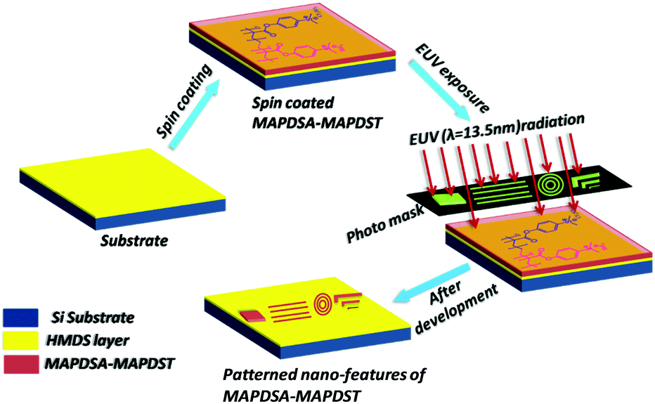 | ||
| Fig. 1 Schematic diagram of the EUVL patterning process employed for the 1.5% and 2.15% resists. | ||
 | ||
| Fig. 2 High resolution XPS Sb 3d spectrum: (a) 1.5% resist; (b) 2.15% resist. | ||
 | ||
| Fig. 3 FE-SEM and HR-AFM images of EUV exposed MAPDSA–MAPDST hybrid resist patterns: (a) 70–20 nm (L/5S) line features of the 1.5% resist; (b) 20 nm (L/5S–L/2S) line patterns of the 1.5% resist; (c) higher resolution 20 nm (L/4S and L/3S) line features of the 1.5% resist; (d) 90–20 nm (L/5S) line features of the 2.15% resist; (e) 20 nm (L/5S–L/2S) line patterns of the 2.15% resist; (f) higher resolution 20 nm (L/4S and L/3S) line features of the 2.15% resist. | ||
Complex nano-features such as boats, waves, line/star-elbow connections, rings, dots etc., have received great interest in the micro/nano electronic industry. This is due to their several advantages in diverse fields including photonic crystals, information storage, high-density magnetic recording, micro-lens arrays, tissue engineering, catalysis and so on.36,38 All the complex nano-features patterned from the 1.5% and 2.15% resists were well characterized using a HR-AFM technique and are presented in Fig. 4, and the relevant 3-D images are shown in the ESI,† Fig. S19. The 40 nm boats, waves and line-elbow connections patterned from the 1.5% and 2.15% resists are shown in Fig. 4a and d. In addition, the higher resolution complex nano-rings and nano-dots (34–50 nm) are presented in Fig. 4b, e, c and f, respectively. The magnified FE-SEM images of some complex nano-features such as star-elbow connections, dots and rings obtained from the 1.5% and 2.15% hybrids are shown in Fig. S20, ESI.† However, efforts to get similar SEM images of the nano-boats/waves were unsuccessful due to poor imaging resolution.
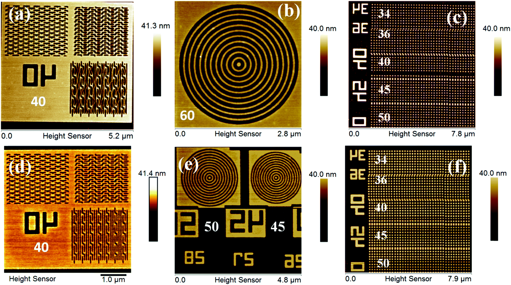 | ||
| Fig. 4 HR-AFM image of EUV exposed complex nano-features: (a) 40 nm boats, waves and line-elbow connections of the 1.5% resist; (b) 60 nm circular patterns of the 1.5% resist; (c) 50–34 nm dots of the 1.5% resist; (d) 40 nm boats, waves and line-elbow connections of the 2.15% resist; (e) 45 and 50 nm circular patterns of the 2.15% resist; (f) 50–34 nm dots of the 2.15% resist. | ||
In order to estimate the potentials of the 1.5% and 2.15% resist formulations as front-line resists for next generation EUVL applications, the sensitivity and contrast (γ) values were computed from normalized remaining thickness (NRT) curve analyses. Here, the residual thicknesses of the 1.5% and 2.15% resists were plotted as a function of varying exposure dose, as shown in Fig. 5. In both cases, a gradual increase in the residual film thickness was observed with increasing exposure dose values. This observation confirmed the negative tone nature of the 1.5% and 2.15% resists. The calculated sensitivity and contrast values for the 1.5% and 2.15% resists were 58.1 mJ cm−2 & 0.036 and 24.5 mJ cm−2 & 0.07, respectively. A small increase in the percentage of MAPDSA units in the case of the 2.15% resist as compared to the 1.5% resist helped to enhance the overall sensitivity, probably due to the increase in the inorganic content (SbF6−) of the hybrid resist, as expected. In addition, in contrast to the sensitivity of poly-MAPDST homo-polymer photoresis36 and other commercially available traditional photoresists,39 the acceptable EUV sensitivity exhibited by the 1.5% and 2.15% resist formulations for patterning high resolution nano-dense lines and complex nano-features provides a path-forward for the design of n-CARs to meet the targets set by ITRS-2015 for NGL applications.
 | ||
| Fig. 5 NRT vs. EUV dose characteristics of the 1.5% and 2.15% resists. | ||
The designed hybrid copolymers (1.5% and 2.15% resists) are mainly based on the radiation/photon sensitive sulfoniumtriflates/antimonates. An initial photodynamic study was carried out using synchrotron radiation as an excitation source (103.5 keV) in order to simulate the EUVL. High surface sensitive analytical tools (NEXAFS and XPS spectroscopy) were utilized for assessing changes following the exposures. The investigation seems to indicate a polarity switching mechanism from hydrophilic sulfonium triflates to hydrophobic aromatic sulfides due to the effect of radiation followed by post bake.35,40 These emergent structural changes lead to negative tone patterning upon the development of the exposed thin films with hydrophilic TMAH developer.40 The inorganic SbF6− moiety is possibly contributing to the enhanced sensitivity due to the higher optical density of Sb (8–10 relative to the carbon optical density of 0–2).33 This is hypothesized based on the higher sensitivity of the copolymer compared to the base MAPDST homo polymer. Further investigations are in progress and will be reported subsequently as part of our continuing work.
The present 1.5% and 2.15% resist polymers are made up of photoactive sulfonium triflates/antimonates. Therefore, during irradiation, these polymers can undergo direct photodecomposition, leading to structural transformations as the resist structures change from polar to non-polar.35,36,40 Thus, these polymers belong to the class of non-chemically amplified resists. However, we also utilized MAPDST as a photo acid generator (PAG) for CAR applications in a separate study.41 During exposure, sulfonium triflates of MAPDST can undergo photodecomposition and release triflic acid products that can induce structural transformations in CARs through a solid state deprotection mechanism.41,42
Conclusions
To conclude, two negative tone hybrid n-CARs, 1.5%-&2.15%-MAPDSA–MAPDST, having different percentages of the hybrid monomer MAPDSA have been synthesized and characterized. The nano-patterning abilities of these hybrid polymers were systematically investigated under high resolution EUVL conditions. The incorporation of a hexafluoroantimonate moiety into the polymer network significantly enhanced the sensitivity of these newly developed hybrid resists as compared to the pristine poly-MAPDST resist. High resolution 20 nm lines as well as various complex nano-features, including waves, boats, dots, rings, line/star-elbow connections etc., have been successfully patterned with the 1.5% and 2.15% resists. All these experimental results support the potential candidature of MAPDSA–MAPDST resists for patterning lower node nano-features using EUVL.Conflicts of interest
There are no conflicts to declare.Acknowledgements
The authors thankfully acknowledge Intel Corp. USA for partial support of the project administered by SRC USA. The use of the Microfield Exposure Tool (MET) at LBNL is also gratefully acknowledged. P. G. Reddy thanks the Council of Scientific and Industrial Research (CSIR), New Delhi, India, for a Senior Research Fellowship. KEG acknowledges Prof. Weibel, UFRGS Brazil, for the photodynamic studies.Notes and references
- G. Moore, Electronics, 1965, 38, 114 Search PubMed.
- H. P. Alesso and C. F. Smith, Connections: patterns of discovery, John Wiley & Sons, New Jersey, 2008 Search PubMed.
- S. Ghosh, C. P. Pradeep, S. K. Sharma, P. G. Reddy, S. P. Pal and K. E. Gonsalves, RSC Adv., 2016, 6, 74462 RSC.
- L. Li, X. Liu, S. Pal, S. Wang, C. K. Ober and E. P. Giannelis, Chem. Soc. Rev., 2017, 46, 4855 RSC.
- R. F. Pease and S. Y. Chou, Proc. IEEE, 2008, 96, 248 CrossRef CAS.
- D. P. Sanders, Chem. Rev., 2010, 110, 321 CrossRef CAS PubMed.
- F. Watt, A. A. Bettiol, J. A. Vankan, E. J. Teoand and M. B. H. Breese, Int. J. Nanosci., 2005, 4, 269 CrossRef CAS.
- A. S. Gangnaik, Y. M. Georgiev and J. D. Holmes, Chem. Mater., 2017, 29, 1898 CrossRef CAS.
- N. Mojarad, M. Hojeij, L. Wang, J. Gobrecht and Y. Ekinci, Nanoscale, 2015, 7, 4031 RSC.
- B. Wu and A. Kumar, J. Vac. Sci. Technol., B, 2007, 25, 1743 CAS.
- S. Inoue, T. Amano, T. Itani, H. Watanabe, I. Mori, T. Watanabe, H. Kinoshita, H. Miyai and M. Hatakeyama, Adv. Opt. Technol., 2012, 1, 269 CAS.
- B. Wu and A. Kumar, Appl. Phys. Rev., 2014, 1, 011104 Search PubMed.
- N. Mojarad, J. Gobrecht and Y. Ekinci, Sci. Rep., 2015, 5, 9235 CrossRef CAS PubMed.
- H. Ito, Adv. Polym. Sci., 2005, 172, 37 CrossRef CAS.
- S. A. M. Donald, C. G. Willson and J. M. J. Frechet, Acc. Chem. Res., 1994, 27, 151 CrossRef.
- M. D. Stewart, K. Patterson, M. H. Somervell and C. G. Willson, J. Phys. Org. Chem., 2000, 13, 767 CrossRef CAS.
- E. Reichmanis and L. F. Thompson, Chem. Rev., 1989, 89, 1273 CrossRef CAS.
- J. W. Thackeray, J. Micro/Nanolithogr., MEMS, MOEMS, 2011, 10, 033009 CrossRef.
- P. P. Naulleau, C. N. Anderson, L. M. Baclea-an, P. Denham, S. George, K. A. Goldberg, G. Jones, B. Mc Clinton, R. Miyakawa, S. Rekawa and N. Smith, Proc. SPIE, 2011, 7972, 797202 CrossRef.
- W. Yayi, B. Markus, D. W. Dieter, L. Antje and S. Michael, Proc. SPIE, 2007, 6519, 65190R CrossRef.
- ITRS, The International Technology Roadmap for Semiconductors, 2015, available via the Internet at https://www.semiconductors.org/clientuploads/Research_Technology/ITRS/2015/0_2015%20ITRS%202.0%20Executive%20Report%20(1).pdf.
- M. Neisser and S. Wurm, ITRS Lithography Roadmap: 2015 Challenges, Adv. Opt. Technol., 2015, 4, 235 Search PubMed.
- A. Grenville, J. T. Anderson, B. L. Clark, P. D. Schepper, J. Edson, M. Greer, K. Jiang, M. Kocsis, S. T. Meyers, J. K. Stowers, A. J. Telecky, D. D. Simone and G. Vandenberghe, Proc. SPIE, 2017, 9425, 94250S Search PubMed.
- K. Kasahara, H. Xu, V. Kosma, J. Odent, E. P. Giannelis and C. K. Ober, Proc. SPIE, 2017, 10143, 1014308 CrossRef.
- K. J. Lawrie, I. Blakey, J. P. Blinco, H. H. Cheng, R. Gronheid, K. S. Jack, I. Pollentier, M. J. Leeson, T. R. Younkin and A. K. Whittaker, J. Mater. Chem., 2011, 21, 5629 RSC.
- V. C. Tejero, S. Carrasco, F. N. Villoslada, J. L. G. Fierro, M. C. C. C. Sanchez, M. C. M. Bondi and C. A. Barrios, J. Mater. Chem. C, 2013, 1, 1392 RSC.
- X. Shi, P. Prewett, E. Huq, D. M. Bagnall, A. P. G. Robinson and S. A. Boden, Microelectron. Eng., 2016, 155, 74 CrossRef CAS.
- H. H. Solak, Y. Ekinci, P. Käser and S. Park, J. Vac. Sci. Technol., B, 2007, 25, 91 CAS.
- J. Fujita, Y. Ohnishi, Y. Ochiai and S. Matsui, Appl. Phys. Lett., 1996, 68, 1297 CrossRef CAS.
- N. Niina, H. Kudo, H. Oizumi, T. Itani and T. Nishikubo, Thin Solid Films, 2013, 534, 459 CrossRef CAS.
- J. Zhang, K. Cao, X. S. Wang and B. Cui, Chem. Commun., 2015, 51, 17592 RSC.
- J. Passarelli, M. Murphy, R. D. Re, M. Sortland, J. Hotalen, L. Dousharm, R. Fallica, Y. Ekinci, M. Neisser, D. A. Freedman and R. L. Brainard, J. Micro/Nanolithogr., MEMS, MOEMS, 2015, 14, 043503 CrossRef.
- M. Sortland, J. Hotalen, R. D. Re, J. Passarelli, M. Murphy, T. S. Kulmala, Y. Ekinci, M. Neisser, D. A. Freedman and R. L. Brainard, J. Micro/Nanolithogr., MEMS, MOEMS, 2015, 14, 043511 CrossRef.
- O. Yildirim, E. Buitrago, R. Hoefnagels, M. Meeuwissen, S. Wuister, G. Rispens, A. V. Oosten, P. Derks, J. Finders, M. Vockenhuber and Y. Ekinci, Proc. SPIE, 2017, 10143, 101430Q CrossRef.
- V. S. V. Satyanarayana, F. Kessler, V. Singh, F. R. Scheffer, D. E. Weibel, S. Ghosh and K. E. Gonsalves, ACS Appl. Mater. Interfaces, 2014, 6, 4223 CAS.
- S. Ghosh, V. S. V. Satyanarayana, B. Pramanick, S. K. Sharma, C. P. Pradeep, I. M. Reyes, N. Batina and K. E. Gonsalves, Sci. Rep., 2016, 6, 22664 CrossRef CAS PubMed.
- Y. Wu, L. Assaud, C. Kryschi, B. Capon, C. Detavernier, L. Santinaccicand and J. Bachmann, J. Mater. Chem. A, 2015, 3, 5971 CAS.
- P. G. Reddy, S. P. Pal, P. Kumar, C. P. Pradeep, S. Ghosh, S. K. Sharma and K. E. Gonsalves, ACS Appl. Mater. Interfaces, 2017, 9, 17 CAS.
- R. Gronheid, H. H. Solak, Y. Ekinci, A. Jouve and F. V. Roey, Microelectron. Eng., 2006, 83, 1103 CrossRef CAS.
- V. Singh, V. S. V. Satyanarayana, N. Batina, I. M. Reyes, S. K. Sharma, F. Kessler, F. R. Scheffer, D. E. Weibel, S. Ghosh and K. E. Gonsalves, J. Micro/Nanolithogr., MEMS, MOEMS, 2014, 13, 043002 CrossRef.
- S. Nandi, M. Yogesh, P. G. Reddy, S. K. Sharma, C. P. Pradeep, S. Ghosh and K. E. Gonsalves, Mater. Chem. Front., 2017, 1, 1895–1899 RSC.
- M. Wang, C. T. Lee, C. L. Henderson, W. Yueh, J. M. Roberts and K. E. Gonsalves, J. Mater. Chem., 2008, 18, 2704–2708 RSC.
Footnote |
| † Electronic supplementary information (ESI) available. See DOI: 10.1039/c7qm00343a |
| This journal is © the Partner Organisations 2017 |