Transport properties of single-component organic conductors, TED derivatives†
Yuka
Kobayashi
 *a,
Jean-Baptiste
Vaney
b,
Takao
Mori
 b,
Yoshitaka
Matsushita
 c,
Takeshi
Terauchi‡
a,
Yoshihiko
Takeda
 d and
Shinjiro
Yagyu
 b
b
aResearch Center for Functional Materials, National Institute for Materials Science (NIMS), Ibaraki 305-0047, Japan. E-mail: kobayashi.yuka@nims.go.jp
bInternational Center for Materials Nanoarchitectonics, National Institute for Materials Science (NIMS), Ibaraki 305-0044, Japan
cMaterials Analysis Station, National Institute for Materials Science (NIMS), Ibaraki 305-0047, Japan
dResearch Center for Advanced Measurement and Characterization, National Institute for Materials Science (NIMS), Ibaraki 305-0003, Japan
First published on 11th October 2017
Abstract
Narrow-gap semiconductors with high conductivity and mobility are an important class of materials for various applications, especially for thermoelectric and optical device applications. Herein, we designed and synthesized novel organic narrow-gap semiconductors, which are modified forms of the main skeleton of a single-component pure organic metal, tetrathiafulvalene-extended dicarboxylate (TED). Molecular design of the TED derivatives with substituent groups on the skeleton led to highly-conducting semiconductors even when powder crystalline samples were used. Their thermopower is greater than that of metallic TED without a substituent group, demonstrating the successful tuning of carrier concentration in the TED system by molecular design. Near-/middle-infrared (IR) diffuse reflectance measurements revealed each band gap, and optical parameters extracted from the spectra evaluated the carrier concentration and mobility of the TED derivatives with fitting calculations on the basis of a Drude–Lorentz dielectric function.
Design, System, ApplicationMost thermoelectric and optoelectric materials for practical use are currently composed of inorganic narrow-gap semiconductors, due to the difficulties in designing narrow-gap molecular systems with high conductivity to achieve good performance. Tetrathiafulvalene-extended dicarboxylate (TED) is a recently developed single-component pure organic metal, which is chemically stable and exhibits high conductivity even with disordered structures. The high carrier concentration in TED is considered to originate from a specific intermolecular charge transfer (CT) interaction between the donor and acceptor sites coexisting in its molecular structure. Therefore, modification of the TED skeleton with substituent groups, namely, design of TED derivatives, which induces a mismatched length between the donor and acceptor sites, offers a possibility to reduce the carrier concentration of the metallic TED and to make the derivatives narrow-gap semiconductors with relatively high conductivity, which is advantageous for thermoelectric and optoelectric performances. Here, we demonstrate the first approach for tuning the carrier concentration and transport properties of a single-component TED system by molecular design. |
Introduction
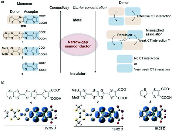
The semi-conducting properties of materials based on their characteristic band gap and carrier concentration have been used in the development of many important physical devices that are responsive to external stimuli, and these devices are used in innovative ways to create modern technologies. Inorganic semiconductors such as doped Si are the most commonly used materials at present because they have many advantages for device applications: high conductivity, mobility and tunable carrier concentration.1 On the other hand, organic semiconductors have recently been attracting keen interest because they exhibit great potential for printable electronics applications.2 Printable technologies for fabricating electronic devices are expected to greatly improve the efficiency of their process and reduce their costs, but this is difficult to achieve using inorganic compounds. Organic compounds are fundamentally insulators, so it is quite simple to design wide-gap semiconductors by utilizing delocalized π electrons in aromatic or conjugated compounds. Therefore, a lot of organic wide-gap semiconductors have been developed so far, mainly for organic field-effect transistors and solar cells.3 On the other hand, molecular design for narrow-gap semiconductors has not been well established so far. The difficulty lies in generating charge carriers in organic compounds by molecular design. The doping technique, which works in π-conjugated conducting polymers, is not usually well adopted in low-weight mass molecules. One possible way to obtain narrow-gap semiconducting molecules is to use radical molecules, which generally possess a lower band gap due to their lower energy level in the lowest occupied molecular orbital (LUMO) compared with those of closed-shell molecules.4 However, tuning of the band gap of radical molecules in the solid state by molecular design is difficult because the band gap is determined not only by the electronic state of a single molecule, but also by a three-dimensional molecular array, which is normally unpredictable.TED is a single-component pure organic conductor that exhibits metallic conduction in itself without any doping by addition of an external reagent.5 TED is prepared via a solution process only, and moreover, high conductivity is achieved even with crystallographically disordered structures such as conducting polymers.6 Therefore, this system has great potential for electronic device applications for use in printed molecular electronics. If transport properties such as the band gap and carrier concentration could be tuned by further molecular design of TED, it would be a powerful strategy for developing new electroactive molecules such as thermoelectric7 and optoelectronic materials,8etc. like inorganic semiconducting systems and conducting polymers. Although metallization mechanism of TED has not been experimentally verified so far, molecular orbital calculations suggest that the large dipole moment of TED likely lets itself being arrayed so as to cancel out the individual moment and induce the delocalization of electrons in the solid state. Its characteristic spin density gradient shows that one side of TTF with dicarboxylate in the TTF–TTF moiety of TED plays the role of an acceptor and the other side acts as a donor, possibly affording intermolecular CT interaction to delocalize molecular spin, which gives rise to high conductivity.5 This observation leads to a new molecular design: TED derivatives with substituent groups, 1 and 2 (Fig. 1a). As our expectation, these groups extend the donor site of TED to tune the transport properties by adjusting the degree of the intermolecular CT interaction, with the intention of being able to control the band gap and carrier concentration. Molecule 3 was designed without the donor site in order to understand the role of intermolecular CT interaction in the electronic state and its transport properties. Molecular orbital calculations predict that the TED derivatives, 1–3, possess a large dipole moment and localized spin density on one side of the TTF–TTF moiety with dicarboxylate (Fig. 1b) as well as those of TED.5
The conductivity and thermopower of the TED derivatives, 1–3, demonstrate the effect of molecular design on the intermolecular CT interaction in these single-component organic conductors. Optical analyses on the basis of NIR/MIR diffuse reflectance measurements clarify the transport properties of the conductors by evaluating their carrier concentration and mobility.
Results and discussion
Preparation of materials
1–3 were prepared via hydrolysis of their insulating precursors, dicarboxylic acid methyl ester forms (Fig. 2a). The preparation of the precursors was carried out following the literature.9 Their hydrolysis quantitatively proceeded via addition of HCl (aq.) (see the ESI†), and this process led to the generation of molecular spins. The electroactive 1–3 are obtained as polycrystalline solids, the purity of which has been confirmed by high-resolution mass spectroscopy (ESI†). The molecular spins were analyzed by electron spin resonance (ESR) measurements (Fig. 2b). The g-values are 2.00639, 2.00630 and 2.00654 for 1, 2 and 3, respectively. The values are slightly larger than 2.00530 of the TTF–TTF˙+ moiety in metallic TED5 but fairly close to 2.00690 of the TTF˙+ moiety in the TTFCOONH4 semiconductor.10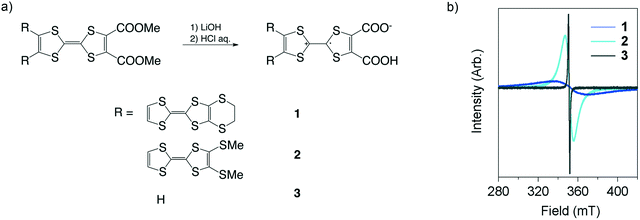 | ||
| Fig. 2 Synthesis and characterization of TED derivatives (1–3). a) Synthetic scheme. b) ESR charts, measured for polycrystalline samples at rt. | ||
Transport properties
Self-standing films were prepared in order to carry out transport measurements, the thickness of which is several μm. Four-probes of Au wires were attached to the films using Au paste as contacts. The electrical conductivity was measured from 260 to 300 K in a He cryostat, and all samples exhibit activation-type transport (Fig. 3). The plots of 1–3 are well fitted with the Arrhenius equation, exhibiting typical semiconducting behaviour obeying the band model in the temperature range. The conductivity at room temperature (rt) (σrt) and activation energy (Ea) are 7 S cm−1 (56 meV) for 1, 1 S cm−1 (94 meV) for 2 and 0.1 S cm−1 (78 meV) for 3. 1 and 2 exhibit very high conductivity as organic semiconductors,11 even including the effects of the grain boundary in the polycrystalline samples. Indeed, 1 is at the highest level among all reported organic semiconductors. The conductivity of 3 is smaller than those of 1 and 2, which demonstrates the positive role of the TTF–TTF skeleton in achieving high conductivity. The Ea of 1–3 is fairly small in radical semiconductors.12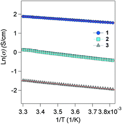 | ||
| Fig. 3 Electrical conductivity of 1–3, measured for self-standing films from 260 to 300 K. Red line shows the slope fitted to plots of ln(σ). | ||
Thermopower was measured at rt; the values are 90 and 57 μV K−1 for 1 and 2, respectively. The thermopower of 3 was not successfully determined due to its low chemical stability under thermal measurements, demonstrating another role of the TTF–TTF skeleton, namely, not only the improvement of conductivity but also of chemical stability. The thermopower of 1 and 2 is increased compared with 17 μV K−1 of metallic TED.5 The transport properties of 1 and 2 suggest that the introduction of a longer substituent in the donor part of TED reduces the carrier concentration, which makes the systems semiconducting and endows them with large thermopower.
Structural analysis
Despite our efforts, single crystals of 1–3 could not be prepared, although the precursor compounds of 1 and 2 were obtained as single crystals.9 The XRD patterns of 1–3 were measured at rt, as shown in Fig. 4. The detected peaks are weak, broadened and small in number, which is not sufficient to determine their three-dimensional structures. This means that the molecules are arrayed in a disordered manner, just as much as those in metallic TED.5 It is of interest that the peaks in 1 are rather more broadened than those of the other systems, even though it has the highest conductivity among the three. This situation is also very similar to that of the TED system, exhibiting much broadened XRD peaks compared to those of an analogous conductor with lower conductivity.5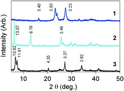 | ||
| Fig. 4 XRD patterns and d values (Å) of 1–3, measured for powder crystals using Cu Kα1 radiation at rt. | ||
Optical analyses
Spectroscopy is one of the most powerful strategies for understanding the electronic properties of electroactive materials13 as well as the strategies such as magnetic measurements14 and band dispersion calculations.15 Optical parameters extracted from the spectra are able to provide important information such as the band gap, carrier concentration, mobility, effective mass, etc. Diffuse reflectance spectra were measured for the three samples in the wavenumber range from 500 to 7500 cm−1. The samples with a thickness of 20–25 μm were measured at 10° and 4° incidence in the NIR and MIR regions, respectively, at rt. The spectra were then converted using the Kubelka–Munk transformation and absorption coefficients were determined.16 A dielectric function on the basis of the Drude model17 and Lorentzian harmonic oscillator model18 was adopted to represent the free-carrier and lattice vibration contributions in the optical response of the materials (eqn (1)). A least-squares fitting of the modeled absorption to the experimental spectra was performed. | (1) |
ε ∞: high-frequency dielectric constant
ω p: plasma frequency
ω 0: damping constant
ω TO: resonance frequency of the transverse optical phonons
S: oscillator strength
Γ: damping constant of the transverse optical phonon.
The squared values of the absorption coefficients multiplied by photon energy (PE) were plotted with respect to PE in eV (Fig. 5a–c) due to the amorphous-like nature of the materials. The band gap was determined from the edge of the absorption peaks to be 0.53, 0.91 and 0.59 eV for 1, 2 and 3, respectively. These are quite small values as compared with organic semiconductors and comparable with those of inorganic narrow-gap semiconductors such as Ge and InN,19 and thus the TED derivatives are categorized as narrow-gap semiconductors. The absorption spectra were well fitted with the dielectric function, eqn (1), in all cases as shown in Fig. 5d–f. The plasma frequency (ωp) was determined from the fitting calculations to the spectra, and the carrier concentration (n), mobility (μ) and effective mass (m*) were evaluated from ωp adopting the following formula,
| ωp = (e2n/4π2c02ε0m*)1/2. |
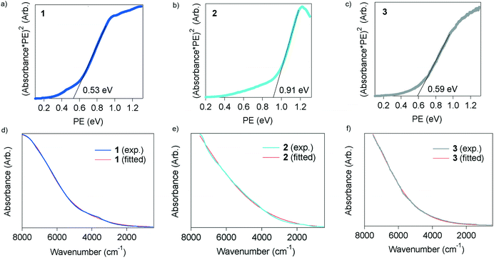 | ||
| Fig. 5 Optical properties of 1–3. a)–c) Absorption spectra plotted with respect to photon energy in eV. d)–f) Absorption spectra measured in the NIR/MIR region at rt and fitted lines with eqn (1). | ||
The parameters are summarized in Table 1. The carrier concentration, n, is 3.20 × 10¹⁹, 2.75 × 10¹⁹ and 3.42 × 1017 cm−3 for 1, 2 and 3, respectively. These are in the range of the carrier concentrations in InN,20,21 GaN (ref. 20) and II–VI semiconductors such as ZnSe and ZnO.20 The mobility of 1 is 1.32 cm2 V−1 s−1, which is one order of magnitude higher than those of 2 and 3. This is consistent with the result that the thermopower of 1 is larger than that of 2, even exhibiting a higher conductivity with a higher carrier concentration. It is of great interest that the m* value of the three is quite small, which is comparable to that of InN in samples with thickness at the μm scale, but their μ is several orders of magnitude smaller than that of InN.21 This fact suggests that thin films which are fabricated with a finely ordered molecular array on a suitable substrate would exhibit higher performance as a semiconductor with higher μ, especially as a thermoelectric material with high conductivity and thermopower.
| ω p (cm−1) | n (cm−3) | μ (cm2 V−1 s−1) | m* | τ (s) | |
|---|---|---|---|---|---|
| 1 | 591.8 | 3.20 × 10¹⁹ | 1.32 | 0.082 | 6.37 × 10⁻¹⁷ |
| 2 | 543.0 | 2.75 × 10¹⁹ | 0.23 | 0.084 | 1.08 × 10⁻¹⁷ |
| 3 | 186.5 | 3.42 × 10¹⁷ | 0.19 | 0.084 | 9.16 × 10⁻¹⁸ |
The mechanism of the reduced carrier concentration in the TED derivatives, leading to their semiconducting properties, is currently unclear. It seems that, however, the long molecular length of the TED skeleton induces some mismatch for the intermolecular CT interaction so as to suppress the generation of free charge carriers. This is to be expected and is in accordance with our conceptual model, as shown in Fig. 1a. This implies that the intermolecular CT interaction, which is controlled by the molecular arrangement by cancelling out the individual dipoles of the molecules, works also in these systems as well as in the metallic TED system.5
Conclusions
TED derivatives with longer or shorter substituents at the TTF moiety were synthesized on the basis of theoretical predictions of their spin density and dipole moment. They exhibited activation-type transport with a room-temperature conductivity of 7, 1 and 0.1 S cm−1 for 1, 2 and 3, respectively. The thermopower of 1 and 2 was 90 and 57 μV K−1, respectively, which were greatly larger than that of metallic TED. Optical analysis confirmed that they are narrow-gap semiconductors with band gaps of 0.53, 0.91 and 0.59 eV for 1, 2 and 3, respectively. The physical properties, n, μ and m* were evaluated from optical fitting calculations. The modification of the TED skeleton succeeded in tuning the transport properties of metallic TED. These results suggest that the TED derivatives could be used in place of inorganic semiconductors in electronic devices that are responsive to external stimuli.Conflicts of interest
There are no conflicts to declare.Acknowledgements
We thank Ms. Kurosawa (NIMS) and Ms. M. Takahashi (NIMS) for assistance in sample preparation and physical measurements. We acknowledge Mr. K. Sasaki (JASCO) and Mr. M. Miura (JASCO) for technical assistance in optical measurements. This study was partially supported by JSPS KAKENHI (Grant Number JP 16K13986).References
- (a) R. S. Pengelly, S. M. Wood, J. W. Milligan, S. T. Sheppard and L. W. Pribble, IEEE Trans. Microwave Theory Tech., 2012, 60, 1764–1783 CrossRef CAS; (b) F. Schaffler, Semicond. Sci. Technol., 1997, 12, 1515–1549 CrossRef CAS.
- (a) Y. Aleeva and B. Pignataro, J. Mater. Chem. C, 2014, 2, 6436–6453 RSC; (b) S. H. Kim, K. Hong, W. Xie, K. H. Lee, S. Zhang, T. P. Lodge and D. C. Frisbie, Adv. Mater., 2013, 25, 1822–1846 CrossRef CAS PubMed; (c) H. E. Katz, Chem. Mater., 2004, 16, 4748–4756 CrossRef CAS.
- (a) P. Verstappen, I. Cardinaletti, T. Vangerven, W. Vanormelingen, F. Verstraeten, L. Lutsen, D. Vanderzande, J. Manca and W. Maes, RSC Adv., 2016, 6, 32298–32307 RSC; (b) W. Wu, Y. Liu and D. Zhu, Chem. Soc. Rev., 2010, 39, 1489–1502 RSC; (c) S. Allard, M. Forster, B. Souharce, H. Thiem and U. Scherf, Angew. Chem., Int. Ed., 2008, 47, 4070–4098 CrossRef CAS PubMed; (d) A. Facchetti, Mater. Today, 2007, 10, 28–37 CrossRef CAS.
- (a) Y. Kobayashi, M. Yoshioka, K. Saigo, D. Hashizume and T. Ogura, J. Am. Chem. Soc., 2009, 131, 9995–10002 CrossRef CAS PubMed; (b) T. Kubo, A. Shimizu, M. Sakamoto, M. Uruichi, K. Yakushi, M. Nakano, D. Shiomi, K. Sato, T. Takui, Y. Morita and K. Nakasuji, Angew. Chem., Int. Ed., 2005, 44, 6564–6568 CrossRef CAS PubMed; (c) S. K. Pal, M. E. Itkis, F. S. Tham, R. W. Reed, R. T. Oakley and R. C. Haddon, Science, 2005, 309, 281–284 CrossRef CAS PubMed.
- Y. Kobayashi, T. Terauchi, S. Sumi and Y. Matsushita, Nat. Mater., 2017, 16, 109–113 CrossRef CAS PubMed.
- (a) A. B. Kaiser, Adv. Mater., 2001, 13, 927–941 CrossRef CAS; (b) J. P. Pouget, et al. , Synth. Met., 1994, 65(2–3), 131–140 CrossRef CAS.
- (a) G. Wang, L. Endicott and C. Uher, Sci. Adv. Mater., 2011, 34, 539–560 CrossRef; (b) F. Freibert, T. W. Darling, T. A. Migliori and S. A. Trugman, Semicond. Semimetals, 2001, 70, 207–244 CAS.
- (a) A. M. Malyarevich, K. V. Yumashev and A. A. Lipovskii, J. Appl. Phys., 2008, 103, 081301 CrossRef; (b) A. Rogalski, Opto-Electron. Rev., 1997, 5, 205–216 CAS; (c) H. Zogg, J. Masek, C. Maissen, S. Blunier and H. Weibel, Thin Solid Films, 1990, 184, 247–252 CrossRef CAS.
- T. Terauchi, S. Sumi, Y. Kobayashi, Y. Matsushita and A. Sato, Cryst. Growth Des., 2014, 14, 1412–1418 CAS.
- K. Furukawa, T. Nakamura, Y. Kobayashi and T. Ogura, J. Phys. Soc. Jpn., 2010, 79, 053701 CrossRef.
- (a) T. Isono, et al. , Nat. Commun., 2013, 4, 1344–1350 CrossRef PubMed; (b) A. El-Ghayoury, et al. , Chem. – Eur. J., 2010, 16, 14051–14059 CrossRef CAS PubMed.
- (a) X. Yu, A. Mailman, K. Lekin, A. Assoud, P. A. Dube and R. T. Oakley, Cryst. Growth Des., 2012, 12, 2485–2494 CrossRef CAS; (b) X. Yu, A. Mailman, K. Lekin, A. A. Assoud, C. M. Robertson, B. C. Noll, C. F. Campana, J. A. K. Howard, P. A. Dube and R. T. Oakley, J. Am. Chem. Soc., 2012, 134, 2264–2275 CrossRef CAS PubMed.
- (a) N. Drichko, M. Dressel, C. A. Kuntscher, A. Pashkin, A. Greco, J. Merino and J. Schlueter, Phys. Rev. B: Condens. Matter Mater. Phys., 2006, 74, 235121 CrossRef; (b) J. Misiewicz, G. Sek, R. Kudrawiec and P. Sitarek, Thin Solid Films, 2004, 450, 14–22 CrossRef CAS.
- (a) P. Bujak, I. Kulszewicz-Bajer, M. Zagorska, V. Maurel, I. Wielgus and A. Pron, Chem. Soc. Rev., 2013, 42, 8895–8999 RSC; (b) L. Balicas, J. S. Brooks, K. Storr, D. Graf, S. Uji, H. Shinagawa, E. Ojima, H. Fujiwara, H. Kobayashi, A. Kobayashi and M. Tokumoto, Solid State Commun., 2000, 116, 557–562 CrossRef CAS.
- (a) I. Vurgaftman, J. R. Meyer and L. R. Ram-Mohan, J. Appl. Phys., 2001, 89, 5815–5875 CrossRef CAS; (b) T. Mori, A. Kobayashi, Y. Sasaki, H. Kobayashi, G. Saito and H. Inokuchi, Bull. Chem. Soc. Jpn., 1984, 57, 627–633 CrossRef CAS.
- (a) L. Schober and H.-G. Löhmannsröben, J. Environ. Monit., 2000, 2, 651–655 RSC; (b) P. Kubelka and F. Munk, Z. Tech. Phys., 1931, 12, 593–601 Search PubMed.
- (a) R. C. Jayasinghe, Y. F. Lao, A. G. U. Perera, M. Hammar, C. F. Cao and H. Z. Wu, J. Phys.: Condens. Matter, 2012, 24, 435803 CrossRef CAS PubMed; (b) P. Drude, Ann. Phys., 1900, 306, 566–613 CrossRef.
- H. A. Lorentz, The Theory of Electrons, Teubner, Leipzig, ch. IV, 1906 Search PubMed.
- J. L. Hudgins, J. Electron. Mater., 2003, 32, 471–477 CrossRef CAS.
- T. V. Blank and Y. A. Gol'dberg, Semiconductors, 2007, 41, 1263–1292 CrossRef CAS.
- E. Tiras, M. Tanisli, N. Balkan, S. Ardali, E. Iliopoulos and A. Georgakilas, Phys. Status Solidi B, 2012, 249, 1235–1240 CrossRef CAS.
Footnotes |
| † Electronic supplementary information (ESI) available. See DOI: 10.1039/c7me00029d |
| ‡ Present address: Department of Chemistry, Tohoku University, Aoba 6-3, Sendai 980-8578, Japan. |
| This journal is © The Royal Society of Chemistry 2017 |

